
Microelectronics world news
Weekly discussion, complaint, and rant thread
Open to anything, including discussions, complaints, and rants.
Sub rules do not apply, so don't bother reporting incivility, off-topic, or spam.
Reddit-wide rules do apply.
To see the newest posts, sort the comments by "new" (instead of "best" or "top").
[link] [comments]
I just detected a real earthquake 😳
 | I just deployed 10 devices all over the city, to detect earthquakes. All devices will send data to server in real-time. When a device detect a shake it will look for other devices if they detect a shake too, when more than 5 detect a shake in the same time frame the server will send a msg to all my family members. So there is no false alarms if someone hit the device or a truck passed a building. This is my first detections for a real P-Wave happened today 300km away. [link] [comments] |
Sound-Powered Sensors Open Another Avenue to Eliminate Batteries
From Labs to Latches, New Autonomous Vehicle Developments Spring Forth
Creating a very fast edge rate generator for testing (or taking the pulse of your scope)

I recently purchased a new oscilloscope for home use. It’s a 250 MHz scope, but I was curious what the actual -3dB frequency was as most scopes have a bit more upper end margin than their published rating. The signal generators I have either don’t go up to those frequencies or, the amplitudes at these frequencies are questionable. That meant I didn’t have a way to actually input a sine wave and sweep it up in frequency until the amplitude dropped down 3 dB to find the true bandwidth. So, I needed another way to find the bandwidth.
Wow the engineering world with your unique design: Design Ideas Submission Guide
You may have seen the technique of using a fast rise time pulse to measure the scope’s bandwidth (you can read how this relation works here). The essence is that you send a pulse, with a fast rising and/or falling edge to the scope and measure the rise or fall time at the fastest sweep rate available. You can then calculate the scopes bandwidth with the Equation (1):

(Note: there is much discussion about the use of 0.35 in the formula. Some claim it should be 0.45, or even 0.40. It really comes down to the implementation of the anti-aliasing filter before the ADC in the scope. If it is a simple single pole filter the number should be 0.35. Newer, higher priced scopes may use a sharper filter and claim the number is 0.45. As my new scope is not one of the expensive laboratory level scopes, I am assuming a single pole filter implying 0.35 as the correct number to use.)
OK, now I needed to find a fast-edged square-wave pulse generator. If we assume my scope has a bandwidth of 300 MHz, then it’s capable of showing a rise time of around:
![]()
The rise time actually seen on the scope will be slower than its maximum because the viewed rise time is a combination of the scope’s maximum rise time and the pulse generator’s rise time. In fact, the relationship is based on a “root sum squared” formula shown in Equation (3):
![]()
Where:
- Rv is the rise time as viewed on the scope
- Rp is the rise time of the pulse generator
- Rm is the scope minimum, or shortest, rise time as limited by its bandwidth
If Rp is much less than Rm, then we may be able to ignore it as it would add very little to Rv. For example, the gold standard for this type of test is the Leo Bodnar Electronics 40 ps pulse generator. If we used this, the formula would show the expected rise time on the scope to be:
![]()
As you can see, in this case the pulse generator rise time contributes a negligible amount to the rise time viewed on the scope.
As nice as the Bondar generator is, I didn’t want to spend that much on a device I would only use a few times. What I needed was a simple pulse generator with a reasonable fast edge—something in the 500-ns-or-better range.
I checked the frequency generators available to me, but the fastest rise time was around 3 ns which would be much too large, so I decided to build a pulse generator. There are a few fast pulse generator designs floating around, some using discrete components and some using Schmitt trigger ICs, but these didn’t quite fit what I wanted. What I ended up designing is based on an Analog Devices LTC6509-80 IC. The spec sheet states it can output pulses with rise time of 500 ps—more on that later. But is 500 ps fast enough? Let’s explore this. What happens if we use a pulse with a rise time in the 500 ns range? Then:
![]()
Even if the final design could attain a 500 ps rise time, this would be too large to ignore as it could give an error in the 10% range. But if we assumed a value for Rp (or better yet pre-measured it) we could remove it after the fact.
As discussed earlier, the rise time that will be seen on the scope can be seen in Equation (1). Manipulating this, we can see that the maximum rise time is:
![]()
So, if we can establish the generator’s rise time, we can subtract it out. In this case “establishing” could be a close enough educated guess, an LTspice simulation, or measuring it on some other equipment. An educated guess is: Based on the LTC6905 data sheet, I should be able to get a ~500 ps rise time in a design. The LTspice path didn’t work out as I couldn’t get a reasonable number out of the simulation—probably operator error. I got lucky though and got some short access to a very high-end scope. I’ll share the results later in the article. But first, let’s look at the design. First, the schematic as shown in Figure 1.

Figure 1 Schematic 1 with the LTC6905 IC to generate a square wave, a capacitor, resistor, and a BNC connector.
The first thing you may notice is that it is very simple: an IC, capacitor, resistor, and a BNC connector. The LTC6905 generates square waves of a fixed frequency and a fixed 50% duty cycle. The version of the IC that I used produces an 80, 40, or 20 MHz output depending on the state of pin 4 (DIV). In this design, this pin is grounded which selects a 20 MHz output. The 33 Ω resistor is in series with the 17 Ω internal impedance thereby producing 50 Ω to match the BNC connector impedance. Matching the impedance reduces any overshoot or ringing in the output. (Using the Tiny Pulser on a 50 Ω scope setting will result in an output 50 mA peak or ~25 mA average output current. It seemed like it might be high for the IC but the spec for the LTC6905 states that the output can be shorted indefinitely. I also checked the temperature of the IC with a thermal camera, and it was minimal.)
I also tried some designs using various resistor values and some with a combination of resistors and capacitors, in series, between pin 5 and the BNC. The idea here was to reduce the capacitance as seen by the IC output. The oscilloscope has an input impedance of around 15 pF (in parallel with 1 MΩ) and adding a capacitor in series could reduce this, as seen by the IC. These were indeed faster but with significant overshoot.
So, Figure 1 is the design I followed through on. The only thing to add to this is a BNC connector, an enclosure (with 4 screws), and a USB cable to power the unit. This simple design, and the fact that the IC is a tiny SOT-23 package, allows for a very small design as seen in Figure 2.

Figure 2 The Tiny Pulser prototype with a 3D printable enclosure based on the schematic in Figure 1 that is roughly the size of a sugar cube.
The 3D printable enclosure is roughly the size of a sugar cube, so I named the device the “Tiny Pulser”. Figure 3 shows the PCB in the enclosure while Figure 4 displays the PCB assembly.

Figure 3 The PCB enclosure of the Tiny Pulser showing the BNC, IC, and passives used in Figure 1.

Figure 4 Tiny Pulser 6-pin SOT-23 PCB assembly with only a few components and jumper wires to solder to the PCB itself.
The PCB is a 6 pin SOT-23 adapter available from various sources (a full BOM is included in the download link provided at the end of the article). As you can see in Figure 4, there are only a few things to solder to the PCB including a jumper. Three wires are attached including the +5 V and ground from the USB cable. The other ground wire needs to be soldered to the BNC body. To do this, I had to break out the old Radio Shack 100 W soldering gun to get enough heat on the BNC base by the solder cup. Scratching up the surface also helped. The PCB is then attached to the BNC by soldering the output pad of the PCB (backside) to the BNC solder cup. (More pictures of this are included in the download.)
So how does it perform? The best performance is obtained when using a 50 Ω scope input and measuring the fall time which was a bit faster than the rise time. In Figure 5 we see the generated pulse train of 20 MHz while Figure 6 is a screenshot showing a fall time of 1.34 ns.

Figure 5 The generated pulse train of 20 MHz of the Tiny Pulser using a 50 Ω scope input.

Figure 6 Fall time measurement (1.34 ns) of the Tiny Pulser circuit made on a 50 Ω scope input.
You can see the pulse train is pretty clean with a bit of overshoot. Note that the 1.34 ns fall time is a combination of the scopes fall time and the Tiny Pulsers fall time. Now we need to figure out the actual fall time of the Tiny Pulser.
As I said I got a chance to use a high-powered scope (2.5 GHz, 20 GS/s) to measure the rise and fall times, Figure 7 shows the results (pardon the poor picture):

Figure 7 Picture of the high-end oscilloscope (2.5 GHz, 20 GS/s) display measuring the rise and fall times of the Tiny Pulser.
You can see that the Tiny Pulser delivers a very clean pulse with a rise time of 510 ps and a fall time of 395 ps. We now have all the information we need to make our bandwidth calculations. (The formulas we have developed are as applicable to fall time as they are to rise time, so we will not change the variable names.) Using the scopes measured fall time and the 395 ps Tiny Pulser fall time, we calculate the bandwidth of the scope, first by calculating the scopes maximum fall time [Equation (6)]:
![]()
And now use this to calculate the bandwidth [Equation (1)]:
![]()
A gut check tells me this is a reasonable number for an oscilloscope sold as a 250 MHz model.
I tested another scope I have that is rated as 200 MHz. It displayed a fall time of 1.51 ns which works out to be 240 MHz. This number agrees to within a few percent of other numbers I have found on the internet. It seems like the Tiny Pulser works well for measuring scope bandwidth!
Another use for a fast pulse
A better-known use for a fast rise time is probably in a time-domain reflectometer (TDR). A TDR is used to measure the length, distance to faults, or distance to an impedance change in a cable. To do this with the Tiny Pulser, add a BNC tee adapter to your scope and connect the cable (coax, twisted pair, zip cord, etc.), to be tested, to one side of the tee adapter (use a BNC to banana jack adapter if needed). Do not short the end of the wire. Next, connect the Tiny Pulser to the other side of the tee adapter as seen in the setup in Figure 8.

Figure 8 A TDR set up using the Tiny Pulser with a BNC tee adapter to connect the circuit as required (e.g., via coax, twisted pair, etc.).
Now power up the Tiny Pulser and adjust the sweep rate to around 10 ns/div so you see something like the upper part of the screen in Figure 9. I find that the high impedance setting on the scope works better than the 50 Ω setting for the wire I was testing. This may vary with the wire you are testing. You can see that the square wave is distorted which is due to the signal reflecting from the end of the wire. If your scope has a math function to display the derivative (or differential) of the trace you will be able to see what’s happening clearer. This can be seen in the lower trace in Figure 9 when I connected a 53 inch piece of 24 AWG solid twisted pair.

Figure 9 Using the high impedance setting on the scope to perform a TDR test on a 53” piece of 24 AWG wire. The math function displays the derivative of the trace to view results more clearly.
To find the timing of the reflection, measure from the start of the pulse rising (or falling) to the distorted part of the pulse where it is rising (or falling) again. Or, if using the math differential function, measure the time from the tall bump to the smaller bump—I find this much easier to see.
In Figure 9 the falling edge of the pulse is marked by cursor AX and the reflected pulse is marked with the cursor BX. On the right side we can see the time between these pulses is 13.2 ns.
The length of the cable or distance to an impedance change can now be calculated but we first need the speed of the wavefront in the wire. For that we need the velocity factor (VF) for the cable that is being tested. This is multiplied by the speed of light to obtain the speed of the wavefront. The velocity factor for some cables may be found here.
In the case of Figure 9, the velocity factor is 0.707. Multiplying this with the speed of light in inches gives us 8.34 inches/ns. So, multiplying 13.2 ns by 8.34 inches/ns yields 110 inches. But this is the time up and down the wire, so we divide this by 2 giving us 55 inches. There are a few inches of connector also, so the answer is very close to the 53 inches of wire.
Note that, because we have a pulse rate of 20 MHz, we are limited to identifying the reflections up to about 22 ns, after which reflection pulses will blend with the next edge generated pulse. This is about 90 inches of cable.
One last trick
An interesting use of the TDR setup is to discover a cable’s impedance. Do this by adding a potentiometer across the end of the cable and adjust the pot until the TDR reflections disappear and the square wave looks relatively restored. Then measure the pot’s resistance and this is the impedance of your cable.
More info
A link to the download for the 3D printable enclosure, BOM, and various notes and pictures to explain the assembly, can be found at: https://www.thingiverse.com/thing:6398615.
I hope you find this useful in your lab/shop and if you have other uses for the Tiny Pulser, please share them in a comment below.
Damian Bonicatto is a consulting engineer with decades of experience in embedded hardware, firmware, and system design. He holds over 30 patents.
Phoenix Bonicatto is a freelance writer.
Related Content
- Exploring software-defined radio (without the annoying RF) – Part 1
- Exploring software-defined radio (without the annoying RF)—Part 2
- Simple GPS Disciplined 10MHz Reference uses Dual PWMs
- Hall effect split-core current sensor calibration station
- 555 triangle generator with adjustable frequency, waveshape, and amplitude; and more!
The post Creating a very fast edge rate generator for testing (or taking the pulse of your scope) appeared first on EDN.
Chiplets diary: Three anecdotes recount design progress

The chiplet design movement representing multi-billion-dollar market potential is marching ahead with key building blocks falling in place while being taped out at advanced process nodes like TSMC’s 3 nm. These multi-die packaging devices can now mix and match pre-built or customized compute, memory, and I/O ingredients in different process nodes, paving the way for system-in-packages (SiPs) to become the system motherboard of the future.
Chiplets also promise considerable cost reduction and improved yields compared to traditional system-on-chip (SoC) designs. Transparency Market Research forecasts the chiplet market to reach more than $47 billion by 2031, becoming one of the fastest-growing segments of the semiconductor industry at more than 40% CAGR from 2021 to 2031.
Below are a few anecdotes demonstrating how chiplet-enabled silicon platforms are making strides in areas such as packaging, memory bandwidth, and application-optimized IP subsystems.
- Chiplets in standard packaging
While chiplet designs are generally associated with advanced packaging technologies, a new PHY solution claims to have used standard packaging to create a multi-die platform. Eliyan’s NuLink PHY facilitates a bandwidth of 64 Gbps/bump on a 3-nm process while utilizing standard organic/laminate packaging with 8-2-8 stack-up.
An efficient combination of compute density and memory bandwidth in a practical package construction will substantially improve performance-per-dollar and performance-per-watt. Moreover, chiplet-based systems in standard organic packages enable the creation of larger SiP solutions, leading to higher performance per power at considerably lower cost and system-level power.

Figure 1 Chiplets in standard packages could encourage their use in inference and gaming applications. Source: Eliyan
Eliyan has announced the tape-out of this die-to-die connectivity PHY at a 3-nm node, and the first silicon is expected in the third quarter of 2024. The tape-out includes a die-to-die PHY coupled with an adaptor layer/link layer controller IP to facilitate a complete solution.
- Sub $1 chiplets
Chiplets have mostly been synonymous with high performance computing (HPC) applications, where these multi-die devices cost tens to hundreds of dollars. YorChip has joined hands with Siloxit to develop a data acquisition chiplet at a sub $1 price target in volume.
The two companies will leverage low-cost die-to-die links, physically unclonable function (PUF) security technology, and delta-sigma analog-to-digital (ADC) IP to create a cost-optimized chiplet. That’s how this chiplet aims to develop a low-cost die-to-die footprint that achieves 75% size savings over the competition.
- High bandwidth memory (HBM) chiplets
Memory bandwidth is a major consideration alongside compute density and high-speed I/Os in chiplet designs. That makes high bandwidth memory 3 (HBM3) PHY a key ingredient in chiplets for applications such as generative AI and cloud computing. This is especially the case in HPC systems where memory bandwidth per watt is a key performance indicator.

Figure 2 The HBM3 memory subsystem supports data rates up to 8.4 Gbps per data pin and features 16 independent channels, each containing 64 bits for a total data width of 1,024 bits. Source: Alphawave Semi
Alphawave Semi has made available an HBM3 PHY IP that targets high-performance memory interfaces up to 8.6 Gbps and 16 channels. This HBM subsystem integrates the HBM PHY with a JEDEC-compliant, highly configurable HBM controller. It has been taped out at TSMC’s 3-nm node and is tailored for hyperscaler and data infrastructure designs.
Related Content
- A sneak peek at chiplet standards
- Bringing Tiny Chiplets To Embedded SoCs
- Intel’s next-generation CPUs hide chiplets inside
- How the Worlds of Chiplets and Packaging Intertwine
- Off-the-Shelf Chiplets Open New Market Opportunities
The post Chiplets diary: Three anecdotes recount design progress appeared first on EDN.
University of Arkansas professor receives $300,000 NSF grant to research gallium oxide-based EV traction inverters
Old analogy gauges
 | I was gifted a box of old analog gauges that I'm trying to figure out what to do with. They look so classic and we're probably great back in their time. Are they worth anything? Does a museum want them? Should I just make a giant display of gauges? Brands include Weston, Ti, Simpson, Honeywell [link] [comments] |
Navitas highlighting GaN and SiC applications at APEC
Cadence Unveils Millennium Platform—Industry’s First Accelerated Digital Twin Delivering Unprecedented Performance and Energy Efficiency
Highlights:
- Revolutionary dedicated HW/SW acceleration platform leverages GPU and CPU computing and proprietary software algorithms to deliver up to 100X design impact through accuracy, speed and scale
- GPU-resident solvers dramatically improve the energy efficiency of simulation by 20X over traditional HPC
- Digital twin, AI and HPC technology combine to provide the best multiphysics simulation solution for automotive, A&D, energy, turbomachinery and data centre markets
- Innovative generative AI technology further accelerates design and analysis exploration, enabling optimal system solutions through superior design insight
- Available for CFD multiphysics analysis today in the cloud or as an on-premises appliance to accommodate customers’ business requirements
Cadence Design Systems, Inc. has announced the Cadence Millennium Enterprise Multiphysics Platform, the industry’s first hardware/software (HW/SW) accelerated digital twin solution for multiphysics system design and analysis. Targeted at one of the biggest opportunities for greater performance and efficiency, the first-generation Cadence Millennium M1 accelerates high-fidelity computational fluid dynamics (CFD) simulations. Available in the cloud or on premises, this turnkey solution includes graphics processing units (GPUs) from leading providers, extremely fast interconnections and an enhanced Cadence high-fidelity CFD software stack optimized for GPU acceleration and generative AI. Millennium M1 instances can be fused into a unified cluster, enabling customers to achieve an unprecedented same-day turnaround time and near-linear scalability when simulating complex mechanical systems.
Designing mechanical systems for new levels of performance and efficiency has become a key priority in the automotive, aerospace and defense (A&D), energy and turbomachinery industries. To optimize performance and reduce greenhouse gases, automotive designers are focused on improving fuel efficiency, reducing drag and noise, and extending electric vehicle range. Increasing efficiency, reducing carbon emissions and reducing maintenance frequency are top of mind for A&D and turbomachinery design engineers. Advances in multiphysics simulation technology are critical to achieving these goals. Performance, accuracy, capacity and accelerated computing are all essential to enabling digital twin simulations that explore more design innovations, providing confidence that they will function as intended before undertaking prototype development and testing.
The Millennium Platform addresses these needs. Highlights and benefits include:
- Performance: Combines best-in-class GPU-resident CFD solvers with dedicated GPU hardware to provide supercomputer-equivalent throughput per GPU of up to 1000 CPU cores
- Efficiency: Reduces turnaround time from weeks to hours with 20X better energy efficiency compared to its CPU equivalent
- Accuracy: Leverages Cadence Fidelity
 CFD solvers to provide unmatched accuracy to address complex simulation challenges
 - High-Performance Computing: Built with an extensible architecture and massively scalable Fidelity solvers to provide near-linear scalability on multiple GPU nodes
- AI Digital Twin: Rapid generation of high-quality multiphysics data enables generative AI to create fast and reliable digital twin visualizations of the optimal system design solution
- Turnkey Solution: The industry’s first solution that couples GPU compute with modern and scalable CFD solvers, providing an optimized environment for accelerated CFD and multidisciplinary design and optimization
- Flexibility: Available with GPUs from leading vendors, in the cloud with minimum 8 GPU configurations, or on premises with a minimum 32 GPU configuration—providing a flexible and scalable solution to fit each customer’s deployment needs
“Throughout our 35-year history, Cadence has been focused on increasing performance with no loss of accuracy for the most challenging computational applications. Algorithmic throughput remains a key priority, and we’re now leveraging generative AI to harvest knowledge gained from massive quantities of design and simulation data,” said Ben Gu, corporate vice president of R&D for multiphysics systems analysis at Cadence. “Our revolutionary Millennium platform is a giant leap forward, delivering unprecedented acceleration and scalability of digital twin and AI applications. CFD is poised to benefit greatly from performance and efficiency gains, and the tremendous power of the Millennium M1 is disrupting industries that must explore more design innovations and bring them to market faster.”
The post Cadence Unveils Millennium Platform—Industry’s First Accelerated Digital Twin Delivering Unprecedented Performance and Energy Efficiency appeared first on ELE Times.
Company was getting rid of some Weller stations.. some new tips and a cleaning and she's good as new
 | submitted by /u/encidius [link] [comments] |
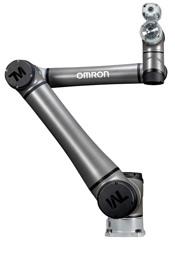
OMRON Automation Launches TM S Series Collaborative Robots with Faster Joints and Expanded Safety Features in India
OMRON Automation has announced the introduction of TM S Series Collaborative Robots in its robotics portfolio in India. This latest addition to OMRON’s innovative lineup combines faster joints and expanded safety features, making it an ideal solution to improve the efficiency of factories in workspaces shared with people.
The new robots are designed to revolutionize industrial automation by enabling a more flexible and productive workspace where humans and robots can collaborate seamlessly. With increased speed and improved performance, the cobots can handle a wide range of tasks, including machine tending, assembly, and packaging. This allows human workers to focus on more complex and value-added activities, ultimately boosting overall productivity and efficiency.
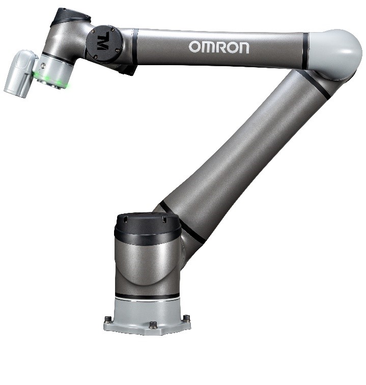
One of the key highlights of the OMRON TM S Series is the enhanced safety features. Built with the latest advancements in safety technology, the cobots are equipped with integrated sensors, collision detection, and collaborative functionality. This ensures a safe working environment for both human operators and robots, eliminating the need for protective barriers and enhancing further collaboration between humans and machines.
“Signifying a significant portfolio expansion to strengthen OMRON’s positioning in the industrial robotics segment, the cobots are ideal for industries like logistics, consumer packaged goods, life sciences, digital hardware, etc. for assembly, palletizing, machine tending, packaging, and pick-and-place tasks. Compact and adaptable, they can be effortlessly relocated for various tasks using its built-in cameras and landmark positioning,” says Sameer Gandhi, MD, OMRON Automation, India.
Traditional factories often face challenges when integrating automation technology due to space constraints and safety concerns. The OMRON TM S Series addresses these issues by providing a flexible and easy-to-implement solution. The compact design makes it suitable for various work environments, even in spaces where traditional robots may not fit. With their small footprint and lightweight structure, they can be seamlessly integrated into existing production setup.
Also, the cobots can be easily programmed and operated using OMRON’s intuitive software, allowing for quick deployment and minimal disruption to existing workflows. The next-gen robot-stick control transforms into a full teach pendant with a touchscreen display. Hand guidance programming helps to convert program to flowchart-based graphical programming and script programming is also available for catering to both novice and advanced users.
The post OMRON Automation Launches TM S Series Collaborative Robots with Faster Joints and Expanded Safety Features in India appeared first on ELE Times.
Debugging SPI be like:
 | submitted by /u/Sleziak0 [link] [comments] |
My proudest kludge yet
 | submitted by /u/Garbage_Can [link] [comments] |
Kioxia First to Release UFS 4.0 Embedded Flash Memory for Automotive
Wi-Fi Certified 7 Is Here. A Wave of Qualified Products Follow Suit
Scope probes reach bandwidths up to 52 GHz

InfiniiMax 4 oscilloscope probes from Keysight operate at bandwidths up to 52 GHz (brickwall response) and 40 GHz (Bessel-Thomson response). The company reports that the InfiniiMax 4 is the first high-impedance probe head operating at more than 50 GHz, making it well-suited for high-speed digital, semiconductor, and wafer applications.

InfiniiMax 4 offers DC input resistance of 100 kΩ differential and two input attenuation settings: high-precision 1-Vpp and high-voltage 2-Vpp maximum input range. The probes work with Infiniium UXR-B series oscilloscopes equipped with 1.85-mm and 1.0-mm input connectors. They are also compatible with the AutoProbe III interface.
The InfiniiMax 4 probes feature an RCRC architecture with a flexible PCA probe head that leverages the natural flexibility of the PCA to take the strain off the delicate tip wires. Their modular probe-head amplifier provides multiple access points, eliminating the need for custom evaluation boards or interposers.
Request a price quote for InfiniiMax 4 oscilloscope probes using the link to the product page below.
Find more datasheets on products like this one at Datasheets.com, searchable by category, part #, description, manufacturer, and more.
The post Scope probes reach bandwidths up to 52 GHz appeared first on EDN.
Low-noise amplifier is radiation-tolerant

Teledyne’s TDLNA0430SEP low-noise amplifier targets space and military communication receivers and radar systems operating in the UHF to S-Band. The radiation-tolerant device offers a low noise figure, minimal power consumption, and small package footprint.

According to the manufacturer, the MMIC amplifier delivers a gain of 21.5 dB from 0.3 GHz to 3 GHz, while maintaining a noise figure of less than 0.35 dB and an output power (P1dB) of 18.5 dBm. The amplifier should be biased at +5.0 VDD and 60 mA IDDQ.
The TDLNA0430SEP low-noise amplifier is built on a 90-nm enhancement-mode pHEMT process. It comes in an 8-pin, 2×2×0.75-mm plastic DFN package and is qualified per Teledyne’s space enhanced plastic flow.
The amp is available now for immediate shipment from the company’s DoD Trusted Facility. An evaluation kit is also available.
Teledyne e2v HiRel Electronics
Find more datasheets on products like this one at Datasheets.com, searchable by category, part #, description, manufacturer, and more.
The post Low-noise amplifier is radiation-tolerant appeared first on EDN.
Flyback switcher ICs boost efficiency

InnoSwitch5-Pro programmable flyback switchers from Power Integrations employ zero-voltage switching and SR FET control to achieve >95% efficiency. A switching frequency of up to 140 kHz and a high level of integration combine to reduce the component volume and PCB board area required by a typical USB PD adapter implementation.

The single-chip switchers incorporate a 750-V or 900-V PowiGaN primary switch, primary-side controller, FluxLink isolated feedback, and secondary controller with an I2C interface. They can be used in single and multiport USB PD adapters, including designs that require the USB PD Extended Power Range (EPR) protocol.
Devices accommodate a wide output voltage range of 3 V to 30 V. To maximize efficiency, the switchers support lossless input line voltage sensing on the secondary side for adaptive continuous conduction mode (CCM), discontinuous conduction mode (DCM), and zero voltage sensing (ZVS) control. A post-production tolerance offset enables constant-current accuracy of <2% to support the Universal Fast Charging Specification (UFCS) protocol.
Prices for the InnoSwitch5-Pro flyback switcher ICs start at $2.40 each in lots of 10,000 units.
Find more datasheets on products like this one at Datasheets.com, searchable by category, part #, description, manufacturer, and more.
The post Flyback switcher ICs boost efficiency appeared first on EDN.
Cortex-M85 MCUs improve motor control

The third group in the Renesas RA8 series of MCUs, RA8T1 devices offer real-time control of motors and inverters used in industrial, building, and home automation. Like other RA8 microcontrollers, the RA8T1 group is based on a 480-MHz Arm Cortex-M85 processor that delivers a performance rating of 6.39 CoreMark/MHz. Arm Helium technology boosts performance by as much as 4X for DSP and ML implementations. This enhanced performance can be used to execute AI functions, such as predictive maintenance.

Optimized for motor control, the RA8T1 32-bit MCUs provide advanced PWM timing features, such as three-phase complementary output, 0% and 100% duty output capability, and five-phase counting modes. On-chip analog peripherals include 12-bit ADCs, 12-bit DACs, high-speed comparators, and a temperature sensor.
The RA8T1 devices integrate up to 2 Mbytes of flash memory and 1 Mbyte of SRAM. Multiple connectivity interfaces are available, such as SCI, SPI, I2C, I3C, CAN/CAN-FD, Ethernet, and USB-FS. In addition, Arm TrustZone technology and Renesas Security IP provide advanced security and encryption.
Offered in 224-pin BGA packages, as well as LQFPs with 100, 144, and 176 pins, the RA8T1 MCUs are available now. Samples and development kits can be ordered on the Renesas website or through the company’s network of distributors.
Find more datasheets on products like this one at Datasheets.com, searchable by category, part #, description, manufacturer, and more.
The post Cortex-M85 MCUs improve motor control appeared first on EDN.
Pages


![[link]](https://i.redd.it/x3dtwa5de4gc1.jpeg)
![[link]](https://i.redd.it/mbpv4yutt3gc1.jpeg)
![[link]](https://i.redd.it/edsz7ta1u2gc1.jpeg)