
Новини світу мікро- та наноелектроніки
Latest issue of Semiconductor Today now available
Lithography specialist ASML decides to stay in Eindhoven, for now

At a time when the semiconductor industry is shrouded in mystery about who is ASML’s second customer of high numerical aperture (NA) extreme ultraviolet (EUV) lithography machine after Intel acquired the first one for its upcoming 14A process node at its fab in Hillsboro, Oregon, ASML has resolved a long-standing matter about its future.
The world’s largest supplier of semiconductor manufacturing equipment has been pondering about moving to another country amid unfavorable business conditions in the Netherlands. Multinationals Shell and Unilever moved their headquarters to London in 2018, citing an unfavorable change in Dutch tax law.

Figure 1 A year after its birth in 1984, ASML moved to a newly built office and factory in Veldhoven, an Eindhoven suburb just a few kilometers from the Philips research labs. Source: ASML
Now ASML—the Netherlands’ largest company and Europe’s largest technology outfit—is having second thoughts due to the government’s immigration policies, housing market shortage, and phasing out of the beneficial tax measures for expats. ASML, which employs 42,000 staff worldwide, has nearly half its workforce based in and around its headquarters in Veldhoven, Netherlands.
It’s important to note that more than 40% of ASML’s 23,000 employees in the Netherlands are not Dutch. In fact, ASML’s initial response was sparked after anti-immigration parties made substantial gains in Netherlands’ 2023 elections. In January 2024, ASML’s then-CEO Peter Wennink warned that his company was highly reliant on skilled foreign labor.
“The consequences of limiting labor migration are large, we need those people to innovate,” he told the press. “If we can’t get those people here, we will go somewhere where we can grow.” That thrust the caretaker cabinet into action, leading to the “Operation Beethoven” initiative to address ASML’s concerns, reported the largest daily newspaper in the Netherlands, De Telegraaf.
The outcome of this government initiative led to a $2.7 billion investment package to improve infrastructure in the Eindhoven region to prevent ASML from moving operations abroad, reported Reuters. The initiative, also aiming to turn Eindhoven into a booming technology hub, will include a large expansion capable of housing 20,000 new employees near Eindhoven’s airport.
The $2.7 billion investment striving to create favorable business conditions for ASML and other Dutch tech outfits will encompass housing, education, transportation, and the electric grid. The infrastructure and highway buildup will also benefit ASML’s headquarters in Veldhoven, a suburb of Eindhoven.
It’s an ambitious undertaking by the Dutch government, and it shows the leverage that successful tech companies have in the socioeconomic context. At the same time, this ambitious expansion plan in Noord-Barbant, an Eindhoven suburb, is merely a letter of intent right now.
That means it’s a long-term undertaking, and that there won’t be any improvements in infrastructure aspects like housing in the short term. “Of course, we have a Plan B, but we want to expand here due to what Veldhoven and Eindhoven have to offer,” said Roger Dassen, ASML’s financial director. “The government also recognizes the circumstances we need to grow.”

Figure 2 The Dutch maker of semiconductor lithography equipment is under immense pressure to maintain its position as an undisputed leader in chip manufacturing gear. Source: ASML
The Dutch paper De Telegraaf, which first reported Operation Beethoven, also mentioned France as a potential destination for ASML’s future expansion. So, while expansion in the Eindhoven region suits ASML because of its existing operations, it has a Plan B in case of failure.
It all comes at a crucial time for the semiconductor lithography titan. It’s nervously charting the opportunity of a lifetime that comes with an unprecedented chip manufacturing boom spanning from Asia to Europe to the United States.
ASML has promptly identified the issues surrounding its future growth, showing its preparedness to fulfill the soaring demand for cutting-edge semiconductor manufacturing equipment. A company spokesperson summed it well by saying that “The decision we need to take is not if we (will) stay, but where we (will) grow.”
Related Content
- ASML Invests $1.9B in Next-Gen EUV
- Moore’s Law Could Ride EUV for 10 More Years
- ASML Ups 2023 Sales Forecast Amid Market Uncertainty
- ASML Warns Chip Shortages to Continue Over Next Two Years
- ASML aims to accelerate EUV platform R&D once SVG merger closes
The post Lithography specialist ASML decides to stay in Eindhoven, for now appeared first on EDN.
STM32CubeMX 6.11 opens its GUI to the boot flash of the STM32H7R and STM32H7S
Author: STMicroelectronics
STM32CubeMX 6.11 is a new milestone as it allows developers to use the unique features of the new STM32H7R and STM32H7S. The software also continues to simplify development on STM32 by offering popular USB middleware previously bound to an OS. Similarly, it is the first version of CMake, which will significantly optimize workflows. STM32CubeMX thus continues to stand as the reference application for STM32 developers thanks to its UI that removes complexity and increases the accessibility of the STM32 ecosystem. Furthermore, the new version inaugurates support for the NUCLEO-U031R8, NUCLEO-U083RC, NUCLEO-H7S3L8, NUCLEO-H533RE.
What’s new in STM32CubeMX 6.11 Support for the STM32H7R and STM32H7SSTM32CubeMX 6.11 is a crucial update for the new STM32H7R and the STM32H7S MCUs because the software helps take advantage of their memory capabilities. Indeed, the devices have a smaller flash, which makes them the most cost-effective STM32H7. Since the device targets applications that must use external storage, the new memory can help significantly lower the bill of materials. Additionally, to make the embedded flash even more meaningful, ST introduced the boot flash, which stores the entire boot sequence, thus replacing the ROM we see on MCUs. Consequently, the embedded storage becomes even more flexible and practical since it isn’t only used for application, but boot, and initialization as well.
To make the boot flash more accessible, we are exposing the feature on STM32CubeMX. Put simply, the GUI will help developers configure the embedded flash to take advantage of its boot capabilities. Similarly, since the STM32H7R and STM32H7S will be used in systems with external memory, STM32CubeMX can set up an external loader so applications like STM32CubeProgrammer can program those discrete flash modules directly. It will also help developers load the main application in the embedded memory and the rest of the system in the external one.
Support for USBX middlewareThe new version of STM32CubeMX adds support for the USBX middleware in a bare metal environment. USBX is a software stack that enables the use of a USB host or device. Until now, developers who wanted to use it had to install ThreadX RTOS. The problem is that if teams wanted to do away with the operating system to optimize their system, they couldn’t use USBX. Thanks to STM32CubeMX, it is now easier to include the right middleware into projects.
Make project generationSTM32CubeMX 6.11 inaugurates its support for CMake, an open-source suite of tools that allow developers to build, test, and package their software. It’s especially useful in large multi-platform projects because it helps streamline large workflows. The current CMake support current focuses on applications that run on a single-core MCU and do not use Trustzone. Over time, we will continue to update our CMake support to allow STM32CubeMX to generate projects for more STM32 microcontrollers.
What is STM32CubeMX?STM32CubeMX is a graphical tool that helps developers generate code that initializes a microcontroller and its application. Users get an interface to configure the MCU’s pinout, resolve conflicts, and set up hardware peripherals and middleware. Users can also configure the clock tree and benefit from a wizard that automates specific calculations. Similarly, it can help set up and tune the DDR on STM32 MPUs. The tool also helps select MCUs or MPUs and download their software packages. Hence, it’s very often the first point of contact with developers. The tool is available in STM32CubeIDE or as a standalone download.
STM32CubeMX also assists developers in other parts of their job. For instance, finding the proper documentation can be tricky, especially with such a vast library. ST is famous for its extensive documentation, and partners tell us that it’s one of the reasons they select our devices. Hence, we offer tutorial videos within the standalone version of STM32CubeMX to help developers search for information. We offer content on configuring the clock tree, the pins, or different software features. Programmers who are new to our tools can start their application quicker, thus further lowering the barrier to entry and reducing friction.
For readers who may be less familiar with STM32CubeMX, here is a rundown of some of the features we’ve released in the past.
A UI for quick feature accessEmbedded system developers must grasp the numerous layers of abstractions within their ecosystem. A typical PC or mobile app developer can do all their work with only one or very few high-level languages and scripting frameworks. Conversely, working with a microcontroller forces teams to consider the many existing layers. For instance, a team looking for the ultimate optimizations will work as close to the metal with low-level code. However, those looking for a more practical approach that can still yield excellent performance will use our hardware abstraction layer (HAL), and those with a priority on rapid development will use our board support package (BSP), which abstracts the HAL.
However, too many embedded ecosystems fail to understand that the higher the abstraction, the more developers seek convenience. Indeed, if teams must spend hours or even days setting up an abstraction layer, it becomes pointless. Consequently, CubeMX 6.10.0 introduced a new UI that helps initialize our BSP functions under “New Projects” -> “Start My Project”. The UI currently works with only a few of our newest development platforms (NUCLEO-C031C6, as well as NUCLEO-H563ZI and NUCLEO-U5A5ZJ-Q when TrustZone is disabled), but our teams are working to support more development boards over time.
Let’s take the example of a blinking light demo on the NUCLEO-H563ZI. The first step is to ensure that at least USER LED GREEN is selected in the Human Machine Interface dropdown menu. When choosing this option in the new UI, the system automatically commits the right pins, instead of just suggesting which pin to use and sets up the HAL so developers can immediately use the BSP function to toggle the LED on or off. Hence, users simply have to push the GENERATE CODE button on the top right side and open the main.c file in Core/Src/ to see the BSP_LED function initialized and ready to use in the main function and ready for use in the while loop.
Additionally, ST included a “Generate demonstration code” option, which adds comments and examples in the generated main C file. Hence, beyond automating the initialization process, the new UI can also serve as a guide for new developers who can open their new files and see how to toggle a light on and off, for instance. Consequently, even a developer with a cursory knowledge of C can run a blinking light application with minimal coaching. In a nutshell, the new version of STM32CubeMX aims to make embedded systems more accessible, even to those with minimal experience in the field.
No admin rights requiredWith version 6.10.0, STM32CubeMX for Windows managed to do away with the admin privilege requirement. Previously, the operating system would ask for the admin password when installing the utility. Now, thanks to a reworking of the installation process, Windows no longer asks for admin permissions, which is a tremendous help for users with a locked-down computer. Often, corporations lock their machines to prevent hacks or misuse, and it can be very cumbersome to ask the administrator to authorize an installation. STM32CubeMX 6.10.0 solved that. The Linux and macOS versions of STM32CubeMX don’t suffer the same issues due to how each operating system manages user privileges.
New support for the STM32H5 and STM32MP13STM32CubeMX is often the first utility developers launch when working on their STM32 MCU because it lets them initialize their device, select the correct firmware package, configure the clock tree, and more. As a result, ST aims to add support for our latest devices continuously. For instance, this new version is compatible with the ability to generate files for secure projects running on our new STM32H5, which introduces new security safeguards. Similarly, STM32CubeMX now provides a memory management tool for the STM32WB and STM32WBA MCUs. The latter is also getting options to support its Thread, Zigbee, and 802.15.4 millimeter wave RF functionalities. Finally, as promised, we are also adding RTOS support for the new STM32MP13.
Memory Management Tool (MMT)STM32CubeMX comes with a Memory Management Tool. The graphical user interface vastly facilitates the configuration of registers on devices like the STM32H5 or STM32U5, among others. For instance, it can help set up a device to use TrustZone, a secure environment, or a memory protection unit with only a few clicks. Previously, developers had to figure out which registers governed what function. The new MMT removes much of the complexity to create a far more intuitive experience. Furthermore, as STM32CubeMX 6.10.0 shows, we continue to bring the MMT to new STM32 devices.
Boot Path ManagementThe Boot Path Manager facilitates the configuration of the new boot loader available on the STM32H5. The latest mainstream MCU from ST supports an immutable root of trust (iRoT) and an updatable root of trust (uRoT). Depending on their security needs, developers can choose to use both, one or none. STM32CubeMX makes this possible by helping users select their configuration from a menu, automatically generate keys, and set up the boot path to secure the microcontroller. As STM32H5 development boards are increasingly available, we ensure that STM32CubeMX can help them take advantage of the new features.
Secure ManagerSecure Manager is another critical feature announced in early 2023 that is now accessible from STM32CubeMX. Secure Manager is our first Trusted Execution Environment. As part of the STM32 Trust initiative, it includes binaries and can help with certification at the system level. As a result, customers targeting a SESIL & PSA Level 3 Certification can vastly hasten their qualification process. In a nutshell, developers use STM32CubeMX to set up all the functionalities in Secure Manager, and the system then uses a scripting mechanism relying on the latest version of STM32CubeProgrammer CLI to configure the MCU.
Pre- and post-flight scriptsST added pre- and post-flight scripting capabilities in STM32CubeMX to automate various tasks. Put simply, users can ask the application to launch scripts before and after it performs a code generation to adapt to the needs of expert users. For instance, a programmer could automatically copy files to a new folder or send them to GitHub before they are erased by the new files generated. It would enable engineers to keep a history of their configuration in case they’d like to revert to a previous state. Similarly, a post-flight script could add the newly generated files to a project and launch an IDE.
Authentication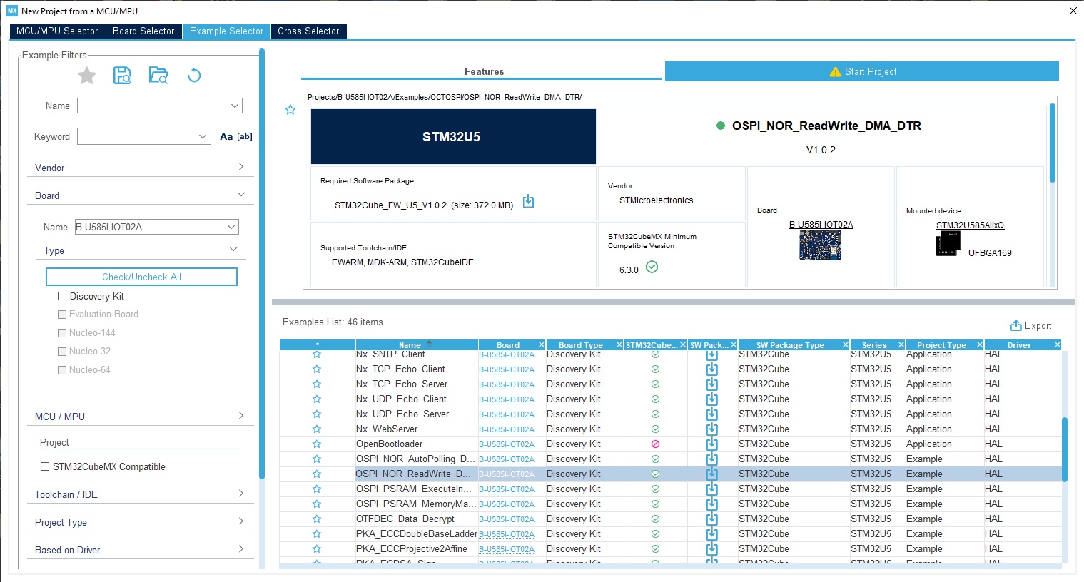 STM32CubeMX
STM32CubeMX requires users to log in to their my.ST.com account before downloading a package, which may perplex some in our community. Previously, users had to leave the application, go to ST.com, and enter their credentials when downloading a piece of software. A few versions ago, STM32CubeMX created a more cohesive experience by ensuring users don’t have to leave the software. However, it does mean asking for their credentials. However, it’s still possible to use STM32CubeMX without an account until that point
The post STM32CubeMX 6.11 opens its GUI to the boot flash of the STM32H7R and STM32H7S appeared first on ELE Times.
Enkris and Incize enter strategic partnership
Easily Incorporate Embedded Security Using Microchip’s PIC32CK 32-bit Microcontrollers with Hardware Security Module
Easily Incorporate Embedded Security Using Microchip’s PIC32CK 32-bit Microcontrollers with Hardware Security Module
The new legislation takes effect in 2024, mandating stricter requirements on cybersecurity on everything from consumer IoT devices to critical infrastructure. Meeting these new security compliance requirements from a product and supply chain perspective can be complex, costly and time-consuming. To provide developers with an embedded security solution that allows them to design applications that comply with these requirements, Microchip Technology announces the new family of PIC32CK 32-bit microcontrollers (MCUs) with an integrated Hardware Security Module (HSM) subsystem and Arm Cortex-M33 core featuring TrustZone technology to help isolate and secure the device.
The PIC32CK SG is the first 32-bit device on the market that combines the strong security of an HSM with TrustZone technology, a hardware-based secure privilege environment. Microchip’s latest innovation for mid-range MCUs provides designers with a cost-effective embedded security solution for their products that meets the latest cybersecurity mandates. The inclusion of an HSM provides a high level of security for authentication, secure debug, secure boot and secure updates, while TrustZone technology provides an additional level of protection for key software functions. The HSM can accelerate a wide range of symmetric and asymmetric cryptography standards, true random number generation and secure key management.
The PIC32CK MCUs from Microchip are designed to support ISO 26262 functional safety and ISO/SAE 21434 cybersecurity standards. For increased flexibility and cost efficiency, the PIC32CK MCU family offers a wide range of options to tune the level of security, memory and connectivity bandwidth based on the end application’s requirements. Options include up to 2 MB dual-panel Flash and 512 KB SRAM, with various connectivity options like 10/100 Ethernet, CAN FD and USB.
“Emerging requirements make security mandatory for the majority of IoT-connected devices. The PIC32CK makes it cost-effective to provide hardware-based security to mid-range microcontroller applications,” said Rod Drake, corporate vice president of Microchip’s MCU32 and MPU32 business units. “Microchip’s ecosystem of tools and security expertise help our customers navigate the complexities of the new requirements and provide lifecycle support for their products.”
For product supply chains that require additional security and safety protection such as in industrial designs, medical devices, home appliances and consumer IoT devices, the PIC32CK will be supported with Microchip’s Trust Platform Design Suite for provisioning as a service. This platform enables the secure factory provisioning of keys, certificates and IP without the need to reveal these secrets within the supply chain.
Development Tools
The 32-bit PIC32CK MCU family is supported by Microchip’s software platforms including MPLAB Harmony v3 and Trust Platform Design Suite. The PIC32CK family is also supported by the PIC32CK SG and PIC32CK GC Curiosity Ultra Development Boards including the EV33A17A and EV44P93A.
The post Easily Incorporate Embedded Security Using Microchip’s PIC32CK 32-bit Microcontrollers with Hardware Security Module appeared first on ELE Times.
Cadence inks partnership with The Royal University of Bhutan to boost VLSI capabilities
Furthering its commitment to foster the next generation of semiconductor talent, Cadence Design Systems (India) Pvt. Ltd., a fully owned subsidiary of Cadence Design Systems, Inc., has signed a memorandum of understanding (MoU) with the College of Science and Technology (CST) at the Royal University of Bhutan. This partnership marks a significant step towards bridging the industry-academic gap by leveraging Cadence’s latest EDA tools to enhance VLSI design capabilities within the college and showcases Cadence’s commitment to providing access to its latest technology tools, even in some of the most remote places in the world.
As a part of this three-year agreement, Cadence will provide research bundle and AWR Design Environment bundle licenses as part of the Cadence University Program to the College of Science and Technology (CST) at the Royal University of Bhutan. This will provide the students and faculty with access to Cadence’s cutting-edge EDA tools, allowing them to delve deeper into the field of VLSI design and facilitating hands-on learning experiences through real-world projects.
The MoU will open new opportunities for internships and placements, enabling students to gain practical industry exposure and refine their skills in preparation for future career endeavours. As a part of this collaboration, Cadence will also provide suggestions on various courses, making them more industry-relevant in alignment with the Cadence University Program.
Speaking on the partnership, Jaswinder Ahuja, Corporate VP – International Headquarters and India Managing Director at Cadence, said, “Through our partnership with the College of Science and Technology at the Royal University of Bhutan, Cadence continues its mission to nurture the semiconductor leaders of tomorrow. By providing access to our cutting-edge EDA technologies, we aim to empower students and faculty to push the boundaries of VLSI design. This collaboration highlights Cadence’s commitment to promoting innovation and bridging the gap between academia and industry.”
“On behalf of the Royal University of Bhutan, I would like to express our sincere gratitude to Cadence for supporting us in our pursuit of excellence in education and research. Integrating Cadence’s cutting-edge EDA tools into our curriculum amplifies our commitment to providing students with a robust, industry-aligned educational journey. We are excited to collaborate with Cadence and empower our future engineers with the expertise and capabilities essential for thriving in the ever-evolving landscape of VLSI design.” – Dasho Nidup Dorji, Vice Chancellor, Royal University of Bhutan
The Cadence University Program grants easy access to the leading electronic design automation tools used for academic research and education to develop advanced users of Cadence technology. Through this program, Cadence aims to train the next generation of innovators, influencing the electronics industry for years to come. Cadence has also partnered with MeitY to provide EDA tools to 104 universities, aiming to create a talent pool of 85,000 engineers in VLSI Design by 2027. Cadence aims to work closely with academic institutions to enhance, improve, and extend the knowledge, capabilities, and expertise of the ecosystem.
The post Cadence inks partnership with The Royal University of Bhutan to boost VLSI capabilities appeared first on ELE Times.
Nuvoton Announces MA35D0 Series MPUs for Industrial Edge Devices
Dual Core, Excels in Security Capabilities, Memory Capacity, and Rich Peripheral
Nuvoton is pleased to announce the NuMicro MA35D0 series, a high-performance microprocessor targeted at industrial edge device applications. The MPU features extensive connectivity and security, which is ideal for smart infrastructure, manufacturing automation, and new energy systems requiring control and networking. Meeting the computing demands of these scenarios, the device is based around dual power-efficient high-performance 64/32-bit Arm Cortex-A35 cores (Armv8-A architecture), running at up to 650 MHz, with 32 KB of L1 instruction and data cache for each core, plus a 512 KB shared L2 cache. The MA35D0 also features high-performance hardware floating-point units (FPU) that enhance its digital signal processing (DSP) capabilities.
To help achieve the cost, performance, size, and energy consumption requirements of its target applications, the MA35D0’s LQFP package, with 128 MB or 256 MB of stacked DDR SDRAM, significantly reduces PCB layer count, device size, BOM cost, and electromagnetic interference (EMI). The chip has an extensive operating temperature (Tj) range from -40°C to +125°C, ensuring reliable operation in challenging edge computing environments.
With all these features, the MA35D0 is well-suited for industrial and other edge and Industrial IoT roles, including factory automation, industrial control, smart buildings, smart homes, smart gateways, and new energy systems.
Extensive Toughened Security Keeps Critical Data Safe
The MA35D0 series can easily establish fast encrypted communications, keep sensitive user data safe, and offer a secure environment for critical applications. The MPU supports secure booting in four modes: USB, SD/eMMC, NAND, and SPI Flash (SPI NOR/SPI NAND).
This chip provides a trusted system that meets the practical security requirements of industrial applications. Arm TrustZone secure boot, and other security features help this MPU safeguard valuable data and code. In addition to TrustZone, it includes Snoop Control Unit (SCU) L2 cache protection and built-in cryptographic accelerators with AES, SHA, ECC, RSA, SM2/3/4—plus a True Random Number Generator (TRNG). The MPU’s cryptographic key store and OTP memory further protect sensitive data.
Wide Choice of Connectivity
For high-performance edge device roles, such as industrial control or gateway applications, the MA35D0 series provides high-speed connectivity and advanced control interfaces, such as 2x megabit ethernet (complying with IEEE 1588 v2), high-speed USB host and device connections, SD3.0/eMMC, 3x CAN FD, and 11x UART. The MA35D0 series also provides touchscreen support and a TFT LCD controller, with resolutions up to 1280×800.
Generous Evaluation and Development Resources
Nuvoton provides rich design resources for the MA35D0 series. The evaluation and development system, the MA35D0 EVB, is pre-loaded with remote control examples, such as browser status access and cloud connectivity, allowing users to begin evaluation and development immediately.
For more information about the MA35D0 series of industrial edge MPUs, please visit https://www.nuvoton.com/products/microprocessors/arm-cortex-a35-mpus/ma35d0-industrial-edge-device-series/
The post Nuvoton Announces MA35D0 Series MPUs for Industrial Edge Devices appeared first on ELE Times.
Got the Ben eater clock kit super excited
 | submitted by /u/Opposite-Sail-7575 [link] [comments] |
Automotive DC motor pre-driver from STMicroelectronics simplifies EMI optimization and saves power
Target applications include electric sunroof, window lift, sliding doors, and power-trunk lift gate
The L99H92 automotive gate driver from STMicroelectronics provides an SPI port for programming and diagnostics, a charge pump, protective features, and two additional current-sense amplifiers for system monitoring.
Containing two high-side and two low-side drivers, the L99H92 can control a single H-bridge powering one bidirectional DC motor or two half bridges for two unidirectional motors. Typical applications for the highly integrated and easily configurable driver include electric sunroof, window lift, powered trunk, sliding doors, and seat-belt pre-tensioners.
The charge pump powers the high-side drivers to maintain correct operation as the vehicle battery voltage fluctuates, enabling the outputs to function with a supply as low as 5.41V. The charge-pump output is also available at an external pin to control a MOSFET for reverse-battery protection.
The gate-driving current is programmed through the SPI port, allowing slew-rate control to minimize electromagnetic emissions and thermal dissipation. Programming the current saves up to four external discrete components per MOSFET, typically needed for slew-rate setting with conventional drivers. The maximum drive current of 170mA gives designers flexibility to use the driver with a wide variety of external MOSFETs, including high-power devices with large gate capacitance.
With many features for system protection and diagnostics, the L99H92 is built for reliability and safety. There is overcurrent protection with a programmable threshold, detected by monitoring the MOSFET drain current. Also, cross-conduction protection with programmable dead time ensures safety and efficiency. Additional protection includes overtemperature early warning and shutdown, overvoltage and undervoltage protection on analog and digital power supply inputs, and open-load and output short-circuit detection in off-state diagnostic mode.
A fail-safe input can turn off all MOSFETs instantaneously and a dedicated diagnostic pin provides immediate fault warning without waiting for periodic SPI transfers.
Additionally, two current-sense amplifiers are integrated for system-status monitoring, helping minimize the bill of materials. Suitable for high-side, low-side, and inline sensing, the amplifiers have independent programmable gain, low offset, and low thermal drift. They can be independently disabled to reduce current consumption when unused.
The L99H92 is in production now and packaged as a TQFP32 or QFN32 with wettable flanks to facilitate inspection. Pricing starts from $1.7062 in the QFN32 package and $1.7246 in the TQFP32 package, for orders of 1000 pieces. For further information please visit: www.st.com/l99h92
The post Automotive DC motor pre-driver from STMicroelectronics simplifies EMI optimization and saves power appeared first on ELE Times.
fixed a Bench power supply today
 | broken transformer, insanely dodgy mains power switch (probably Stolen from a lamp sometime) and a shitty solder Job on a 7805 all added up to the thing ending in the scrap pile. fixing all these things made it work again, have to say is a decent low voltage low current supply. [link] [comments] |
Disclosing the results of a webcam closeup

Remember 2020? Global pandemic lockdown forced many of us out of our cubicles and into haphazard home offices, frantically outfitted and upgraded for their new tasks. Retailer inventories of webcams (and associated green screens), ring lights, microphones, headsets, broadband networking equipment and the like quickly evaporated, boosting the prices of whatever remaining equipment stock scraps were left to stratospheric levels. And both existing and new suppliers, sensing a highly profitable business opportunity, rushed to market with products based on whatever (sometimes subpar) system building blocks they could source.
Four years later, COVID-19 is still with us, of course, but many of us have returned to the cubicles (at least part-time, and sometimes reluctantly). But regardless, we’re now fully gear-equipped at all possible work locations. The electronics supply-vs-demand curve has therefore regained sanity, leading to no-longer-crazy prices. And longstanding webcam (for example) suppliers are differentiating their products, hoping to escape profit-killing commoditization: BenQ with the easily relocatable, macro-capable ideaCam S1 Plus and Pro, for example:
Logitech’s Brio line with a focus (pun intended) on high res and other image enhancements:

And Razer’s Kiyo integrating illumination:

Back to commodities. As I’ve mentioned before, I regularly donate computers, both ones that I’ve personally used and outgrown and others hand-built specifically for this purpose, to a local charity for subsequent handoff to its income- and otherwise-challenged clients. I always make sure that the computers include full online communications capabilities—a microphone, speakers, and a webcam, to be precise—for virtual job interviews, online advanced education classes and the like. With laptops this is easy, since such gear is already built in. For desktop computers, on the other hand, I need to source this stuff separately.
Back in February (as well as several times before, apparently), the Avaya Huddle HC010 Webcam was on sale at bargains site Meh, in this case for $14.99 each. At the time, it was reportedly selling for $60.99 at Amazon (it’s now $39.99 there as I write these words two-plus months later), so I quickly “fished” the three-unit limit (two will eventually end up with charity-donation computers; the third is being dissected here just for you). And longer-term historical data is even more revealing. Back in mid-2021 when the pandemic was still raging and the product was just-introduced, Amazon had it marked at $129 per price-tracking site CamelCamelCamel.

The specs are average and passable:
- 1080p and 720p resolution options, along with a 30 fps frame rate
- A/V output: H.264 over USB 2.0
- Digital (i.e., software-interpolated, and Windows-only) pan, tilt and 4x zoom
- 85° horizontal field of view
- Two integrated microphones
- Built-in privacy cover
- Integrated activity light
- Dimensions of 4.65″ (L) x 1.46″ (W) x 1.22″ (H)
- Weight of 3.28 oz
- 1/2.8″ CMOS image sensor
- 8mm focal length
although low-light performance is generally dubious-at-best with such cost-centric products. Here’s a promo video with more details:
And here’s our victim, beginning with the obligatory outer box shots:

 Note, to my earlier “suppliers sensing a highly profitable business opportunity” comment, the mid-February 2021 manufacturing date:


 Now let’s take a peek inside:

A desiccant packet and two slivers of literature:

Along with (cue striptease music)…

Our patient, as-usual accompanied by a 0.75″ (19.1 mm) diameter U.S. penny for size comparison purposes:


Here’s what it looks like from the front. Note the microphone ports to either side of the currently protected cover/lens, and the currently extinguished activity light above the penny:

Remove the protective sliver of plastic in the center and you can see the privacy cover, marked red to alert you when it’s in place:

versus slid away to reveal the lens behind it:

with both positions controlled by a topside switch:

Here’s the rear (I made a rhyme! I’m easily amused!):

And here’s the bottom, first revealing the ¼” thread tripod base built into the lower segment of the two-piece hinged “foot”:

Unfold the two halves of the “foot” and more product info appears, courtesy of another label (augmenting the already shown one attached to the product packaging):


There’s actually another hinge, this one connecting the “foot” to the main body and convenient for when you need to tilt the webcam down post-mount to more effectively frame the user:


And speak of “mount”, it occurred to me post-disassembly of the Avaya HC010 that some of you might not already be familiar with standalone webcams (versus those built into laptop display bezels) and therefore how they’re mounted to displays. Here’s my woefully dusty Logitech Brio perched on top of my Dell UP2516D two-LCD suite; the HC010 operates similarly:

Onward. The front panel pops off easily:


The translucent rubber piece shown at left in the prior photo fell out as I was pulling the panel off. I put it back in place for the following photo (stay tuned for its function):

We now have our first unobstructed perspective of the insides, once again in both privacy cover-active and-inactive modes:


Note the (inexpensive) electret condenser mics on either side, along with the “hole” into which the other end of the recently mentioned translucent rubber piece fits. The piece’s function, as it turns out, is to act as a sort of “light pipe”, transferring the illumination coming from an embedded-in-hole LED, presumably attached to a PCB-to-be-seen-fully-later, to the front panel.
See, too, those four screws, one in each corner? To proceed further, I first tried removing them:

which didn’t get me anywhere meaningful:

The five additional inner screws, on the other hand…


The aforementioned two-piece “foot” also detached as a result:


Now let’s see if we can get the inside assembly to move:

That’s encouraging:

All that’s left is to detach the USB cable’s power-and-data connector to the PCB:

And out it goes!

with the gasket around each mic coming off in the process:


Here’s a standalone front view of the inner assembly, with most of the PCB still obscured by the black plastic frame:

Top view:

Bottom:

And finally, the now-visible backside:

Four more screws to remove:


And the black plastic frame comes right off. Inside:

Already-seen outside:

And now free-and-clear PCB:

Next, let’s detach those mics:


Note, too, the previously embedded-in-hole LED in the upper left corner of the USB connector:

Bottom-side view:

Top:

Left:

Right:

And now let’s flip the PCB back over and peel off the heat sink you likely already noticed earlier:


The dominant-size square IC now revealed at right has markings too faint to discern in a photo, so you’ll have to take my word that it’s the SSC33x Camera SoC Processor from a company called SigmaStar. The smaller chip in its upper left corner (the one with the dab of blue paint on top of it) is a GigaDevice GD25Q64CSIG 64 Mbit SPI NOR flash memory, presumably containing the system firmware. And in the middle, you probably already noticed two more screw heads:

I’m betting that removing them will enable detach of the lens assembly on the other side of the PCB. Let’s see if I’m right:


Yep, we have liftoff:

Here’s the now-exposed other end of the lens:

And here’s the image sensor!

That wraps it up for today, folks. As always, I welcome your thoughts in the comments!
—Brian Dipert is the Editor-in-Chief of the Edge AI and Vision Alliance, and a Senior Analyst at BDTI and Editor-in-Chief of InsideDSP, the company’s online newsletter.
Related Content
- COVID-19: The long-term implications
- Communication in COVID-19 lockdown: Empowering the tech-challenged
- COVID-19: Our new normal
- Aukey dash cam teardown redux: this time, the DRA5 gets a look
- The Godox V1 camera flash: Well-“rounded” with multiple-identity panache
- Teardown: Blink XT security camera
- Teardown: High-quality and inexpensive security camera
The post Disclosing the results of a webcam closeup appeared first on EDN.
EDA toolset parade at TSMC’s U.S. design symposium

The EDA trio—Cadence Design Systems, Siemens EDA, and Synopsys—is working hands in hand with TSMC to facilitate production-ready EDA tools for the mega-fab’s newest and most advanced processes. These EDA outfits showcased their IC design solutions at the TSMC 2024 North America Technology Symposium held in Santa Clara, California, on 24 April 2024.
The EDA tie-ups with TSMC show how toolmakers have established a symbiotic relationship with large fabs to support chip designers on advanced semiconductor manufacturing nodes. Moreover, it demonstrates why design flow migration is critical when chip designs move from one advanced node to the next.
- Cadence
Cadence showcased its node-to-node design migration flow based on the Cadence Virtuoso Studio, which facilitates the migration of schematic cells, parameters, pins, and wiring from one TSMC process node to another. Next, Virtuoso ADE Suite’s simulation and circuit optimization environment tunes and optimizes the new schematic to ensure the design achieves all required specifications and measurements.
That allows IC designers using Cadence tools on TSMC process nodes to automatically recognize and extract groups of devices in an existing layout and apply them to similar groups in the new layout. Cadence has also been working closely with TSMC to ensure its EDA tools’ compatibility with fab’s advanced nodes, including N3E and N2 process technologies.

Figure 1 The enhanced PDKs and EDA methodologies simplify and accelerate the design migration from one process node to another. Source: Cadence
- Siemens EDA
Siemens EDA displayed its IC design solutions for TSMC’s latest process and advanced packaging technologies, including IC verification tool Calibre nmPlatform now certified for TSMC’s N2 process. At TSMC’s event, Siemens EDA also demonstrated its FastSPICE platform for circuit verification of nanometer analog, RF, mixed-signal, memory; it’s now certified for TSMC’s N3P, N2 and N2P process nodes.

Figure 2 The EDA toolset certifications are crucial in migration to new IC manufacturing process and advanced packaging technologies. Source: Siemens EDA
Siemens EDA also provided details about collaboration with TSMC to certify its Calibre 3DSTACK solution’s support for the foundry’s latest 3Dblox standard. TSMC’s 3Dblox technology addresses specific IC test and diagnosis challenges that arise at 2-nm geometries and below.
- Synopsys
Synopsys also unveiled details about its latest collaborations with the Taiwanese fab, including a co-optimized photonic IC flow, which is integrated with the EDA firm’s 3DIC Compiler and supports TSMC’s 3Dblox technology.

Figure 3 The production-ready design flows were showcased for TSMC’s advanced nodes at the symposium. Source: Synopsys
Additionally, Synopsys showcased its digital and analog design flows compatible with TSMC’s N3/N3P and N2 process nodes. The EDA toolmaker is also working closely with TSMC to ensure the design productivity and optimization of its AI-driven flows such as Synopsys DSO.ai.
Related Content
- TSMC rolls analog design kit, EDA formats
- TSMC taps Cadence to provide DFM services
- TSMC debuts EDA reference flow for SoC designs
- EDA toolmakers prep for TSMC’s N3E and N2 nodes
- Synopsys collaborates with TSMC on 2nm IP portfolio and photonics ICs
The post EDA toolset parade at TSMC’s U.S. design symposium appeared first on EDN.
Raptee Sets the Stage for Two-Wheeler EVs in India
Raptee is a full-stack two-wheeler EV startup with their flagship product highly tech-enabled and IoT-centred. The team began operations out of Chennai in 2019 with a mission to democratise electric mobility in India. They are crafting a two-wheeler EV that is more of an augmented machine which is intelligent, intuitive and safe with features like throttle mapping, blind-spot detection, and Bluetooth connectivity. So far, Raptee has over 31 technological patents in its name.
 Mr. Dinesh Arjun, CEO & Cofounder, Raptee
Rashi Bajpai, Sub-Editor at ELE Times spoke with Mr Dinesh Arjun, CEO and Co-founder at Raptee on various aspects of EV with a prime focus on the Indian market.
This is an excerpt from the conversation.
- Can you throw some light on the go-to features/ major USP of Raptee’s electric motorcycle?
Our bikes come with an onboard charger that plays an essential role in bidirectional charging modes thus making the riding experience hassle-free. Additionally, we stand out as the only electric two-wheeler company in India to leverage the ubiquitous CCS2 charging standard. This compatibility grants you access to the extensive public charging network, allowing you to top up your bike from 0 to 80% in a mere 45 minutes.
- What core technologies and concepts does the team Raptee work on? Please highlight your key expertise and core competencies.
As the sole electric two-wheeler (e2W) utilizing a high-voltage drivetrain, we deliver superior performance surpassing any internal combustion engine (ICE) counterparts. The seamless integration of VCU and cloud computing not only enhances rider experience with smoother acceleration and improved handling but also offers practical benefits like efficient trip planning through real-time battery status updates, showcasing Raptee’s commitment to innovation and practical functionality on the road.
- As India moves towards self-reliance in the area of information and technology, a wave of innovations and ideas has taken over the nation. How well is Raptee prepared to pursue development in the EV sector under the “Make in India” policy?
Raptee substantiates its alignment with the “Make in India” policy through its complete in-house design and development of all components. This comprehensive approach not only ensures technological sovereignty but also fosters a culture of innovation and expertise within the domestic industry. Additionally, Raptee’s establishment of a complete supply chain ecosystem from scratch addresses a critical gap in the market, particularly concerning high-voltage technology. This initiative not only reduces dependency on imports but also enhances the resilience and competitiveness of India’s EV sector.
- What is your view on EV battery swapping booths and can its implementation help India come closer to sustainable electric mobility?
As battery technology evolves, the range of EVs is steadily increasing, reducing the need for frequent charging. This improvement diminishes the perceived advantage of battery swapping, which is often promoted as a quick solution for limited-range EVs. As batteries become more energy-dense and charging times decrease, charging stations become more efficient and comparable in terms of convenience.
- India’s electric two-wheeler (E2W) sector is expected to cross the one million mark in 2024-what are the factors that will influence the market to reach the mark?
India’s E2W market is on an electric revolution, with sales expected to breach the one-million mark in 2024. This surge is driven by a customer-centric approach. Gone are the days of limited choices. Manufacturers are offering diverse options, from high-performance motorcycles to practical everyday rides, catering to every rider’s needs. Range anxiety is fading too, with advancements in battery technology and a rapidly expanding charging network. Additionally, robust customer support with readily available service and informative resources empowers riders, building trust and confidence in E2Ws. This focus on customer satisfaction, coupled with innovation and infrastructure development, is paving the way for a million E2Ws and a sustainable transportation future for India
- How can better implementation of the charging infrastructure accelerate the sales of EVs?
A well-developed charging infrastructure plays a pivotal role in accelerating electric vehicle (EV) sales by addressing critical consumer concerns. Firstly, it alleviates the fear of “range anxiety” among potential buyers by ensuring a widespread network of charging stations along highways and in urban areas, thereby assuring drivers they can recharge conveniently during their journeys. Secondly, the availability of fast-charging stations, such as those utilizing the CCS2 standard, significantly reduces charging times, making EVs more competitive with traditional gasoline vehicles. This not only enables quicker trips but also enhances overall convenience by minimizing wait times at charging stations. Moreover, a robust charging infrastructure sends a powerful message to the public, signaling that EVs are a practical and supported transportation choice. This reassurance can sway hesitant consumers, ultimately driving increased EV adoption.
- Tell us about Raptee’s goals and vision for the next decade.
Raptee’s vision is nothing less than a revolution in personal mobility. We are committed to accelerating the shift towards safe, smart, and sustainable transportation solutions, making them accessible to everyone. Fueled by a deep-tech core, we’re pioneering innovative technologies like HV drivetrains to achieve this ambitious goal.
Our focus isn’t limited to electric vehicles. We see ourselves as architects of the future of mobility, constantly exploring new product landscapes based on customer preferences and inventing disruptive technologies across different segments.
By the next decade, Raptee aspires to be a global leader in personal mobility, with a significant market share. This leadership will be built on the foundation of our unwavering commitment to safety, sustainability, and cutting-edge technological innovation.
The post Raptee Sets the Stage for Two-Wheeler EVs in India appeared first on ELE Times.
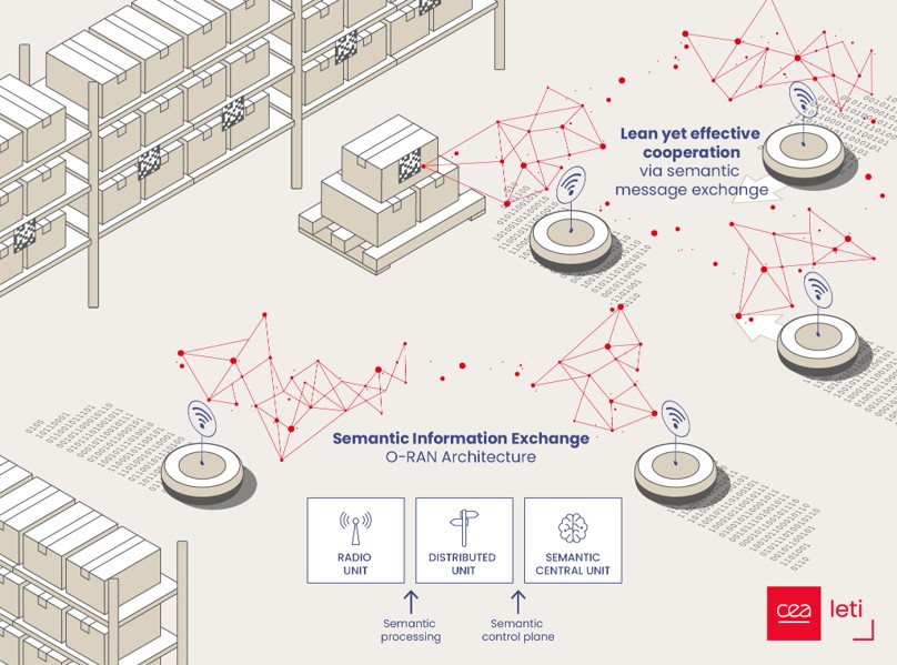
CEA-Leti Selected to Coordinate Two EU Projects for Developing ‘First-Class’ 6G Capabilities and Contributing to Standardization
Engaging Multiple EU Partners, the Projects Will Apply Intelligent Sensing and AI-enabled Learning Technologies
As part of the European Union’s drive to support a multifaceted approach to addressing 6G challenges and promises, CEA-Leti has been chosen to coordinate two projects to help build first-class 6G technology capabilities and boost standardization efforts across Europe.
The two projects were among 27 chosen in a competitive proposal process by an EU partnership that divided €130 million between the projects. “These projects present a significant stride towards advancing smart networks and services, offering breakthrough innovations, experimental platforms and large-scale trials, driving world-class research and shaping the world’s digital connected future,” said the group, called the Smart Networks and Services Joint Undertaking (SNS JU).
6G-DISAC (Distributed Intelligent Sensing and Communication) and 6G-GOALS (Goal-Oriented AI-enabled Learning and Semantic Communication Networks) launched their three-year projects in January with multiple EU collaborators.
The two projects mark the first time a single RTO or company has been chosen to coordinate two competitive EU proposals in the same initiative. CEA-Leti has coordinated several EU projects, including the recently completed RISE-6G project. That SNS JU effort developed a disruptive new concept as a service for wireless environments by dynamically controlling wireless communication for brief, energy-efficient and high-capacity communications on a variety of surfaces, such as such as walls, ceilings, mirrors and appliances.
6G-DISAC
This project will develop and innovate on a widely distributed intelligent infrastructure compatible with both real-world integration constraints, new semantic and goal-oriented communication and sensing approaches, and the flexibility requirements of future 6G networks. It will apply theoretical approaches and operational and standards-compatible, distributed joint communication and sensing, by leveraging the expertise of world-leading network vendors, verticals, SMEs, research laboratories and academic institutions spanning the value chain.
Current approaches to integrated communication and sensing use centralized architectures and pass sensed information through a centralized controller.
“This project will bring the integrated sensing and communication (ISAC) vision into reality, going well beyond the usual restrictive standalone or localised scenarios, by adopting a holistic perspective, with large numbers of connected users and/or passive objects to be tracked,” said Emilio Calvanese Strinati, coordinator of the project and CEA-Leti’s smart devices & telecommunications strategy program director.
“With demonstrations that validate the vital 6G-DISAC concepts, the project will revolutionise various applications, from extended reality and robot-human interaction to vehicular-safety functions and improving communication key performance indicators (KPI) with sensing-aided communications,” he explained.
In addition to defining use cases and designing innovative network architecture, the 11 6G-DISAC partners will develop novel physical-layer waveforms, distributed sensing and communications methods, and optimised resource allocation methods and protocols.
Specific targets include:
- tracking connected user equipment (UE) and passive objects,
- performing ISAC with many distributed base stations, efficient distributed signal processing and machine learning for semantic ISAC, and
- incorporating extremely large multiple-input, multiple-output (MIMO) technologies and reconfigurable intelligent surfaces, and intelligent sensing activation.
“While addressing these fundamental and practical challenges, the team will focus on the distributed implementation of ISAC, unlocking real sensing applications and providing a multi-perspective view of networks in space and time for tangible communication gains,” Calvanese Strinati said.
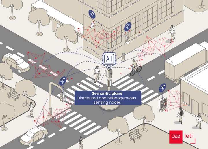
6G-GOALS
This project is designed to reduce data traffic by conveying only the most relevant information and produce data-efficient, robust and resilient protocols that can adapt to network conditions and communication objectives using modern AI/ML techniques.
“As wireless mobile communication requires ever-higher data rates and 5G’s scope expands to include massive and ultra-reliable low-latency links, wireless evolution has been pressed to solve the technical problem of reliable data exchange between two end-points,” said project coordinator Calvanese Strinati.
“The 6G-GOALS project will take the wireless system design to its next stage by considering the significance, relevance and value of the transmitted data and transforming the potential of the emerging AI/ML-based architectures into a semantic and goal-oriented communication paradigm, offering a solid step toward cooperative generative AI technologies,” he said.
Semantic communication is instrumental in inducing reasoning and shared understanding among intelligent agents by exchanging pragmatically selected information in which its meaning to the receiver is designed to efficiently accomplish a goal or a task. With current approaches, data is sensed and transferred from sensors to the destinations without prior semantic extraction functions.
A recent paper written by 6G-GOALS participants noted that advances in AI technologies have expanded device intelligence, fostering federation and cooperation among distributed AI agents. These advancements impose new requirements on future 6G mobile network architectures.
“To meet these demands, it is essential to transcend classical boundaries and integrate communication, computation, control, and intelligence,” the paper, “Goal-Oriented and Semantic Communication in 6G AI-Native Networks: The 6G-GOALS Approach”, reports.
“These projects are fundamental to explore the capabilities of AI/ML solutions on the networks of the future, especially dealing with joint communication and sensing and semantic communications,” said Mauro Boldi Renato, EU project program coordinator at TIM (Telcom Italia). “Working with CEA-Leti represents a solid basis for their success and for bringing European industry towards implementation of 6G around 2030.”
“The exploitation of 6G-DISAC and 6G-GOALS project results will represent a transformative step for manufacturers and 6G industrial players, like NEC Corporation, by fostering the development of distributed intelligent networks and semantic/AI-driven communication strategies,” said Vincenzo Sciancalepore, principal researcher at NEC Laboratories Europe GMBH/ Germany and a member of the 6G-DISAC team. “Such an unprecedented approach will enable more efficient, flexible, and responsive network infrastructures that can support advanced applications, such as extended reality and automated mobility, meeting the increasing demand for high-capacity, low-latency and sustainable communication.”
6G-DISAC Partners
- Coordinator: CEA-Leti/France
- Technical Manager: Chalmers Tekniska Hogskola AB/Sweden
- Innovation Manager: Nokia Networks/ France
- Telecom Italia Spa/Italy
- Orange S.A./France
- Ethniko Kai Kapodistriako Panepistimio Athinon/Greece
- Institut Polytechnique
De Bordeaux/France
- NEC Laboratories Europe GmbH/Germany
- NEC Italia S.P.A/Italy
- Robert Bosch GmbH/Germany
- RadChat AB/Sweden
6G-GOALS Partners
- Coordinator: CEA-Leti/France
- Technical Manager: Consorzio Nazionale Interuniversitario per le Telecomunicazioni/Italy
- Innovation Manager: NEC Laboratories Europe GMBH/ Germany
- NEC Italia S.p.A/Italy
- Telecom Italia S.p.A/Italy
- Eurecom GIE/France
- Aalborg Universitet/Denmark
- Hewlett-Packard/France
- Hewlett-Packard Italiana S.R.L/Italy
- Toshiba Europe Limited UK
- Imperial College of Science Technology and Medicine UK
- Singapore University of Technology and Design
The post CEA-Leti Selected to Coordinate Two EU Projects for Developing ‘First-Class’ 6G Capabilities and Contributing to Standardization appeared first on ELE Times.
maXTouch Touchscreen Controller Family Expands with Additional Security Features for Touchscreen Payment Systems
Microchip’s ATMXT2952TD 2.0 family of touch controllers offer cryptographic authentication and data encryption
As we see an increased number of electric vehicles (EVs) on the road, the necessary charging infrastructure must expand to meet the increased demand. Adding credit card payment options to EV chargers is becoming a standard practice in many countries—and is a mandate in the European Union—and chargers need to meet Payment Card Industry (PCI) security standards. To help EV charger designers protect their payment architectures, Microchip Technology has launched the MXT2952TD 2.0 family of secure touchscreen controllers.
Typical touch-enabled human-machine interface (HMI) and radio frequency identification (RFID) combination-based payment systems are vulnerable to hacking attacks via malicious software updates or man-in-the-middle attacks when a user enters their personal identification number (PIN) on the touchscreen. Physical mesh barriers and sensors are often used around these integrated circuits (ICs) for protection from hacking. Constant reflashing of software and device resets are used to help safeguard software integrity. The MXT2952TD 2.0 family is designed to encrypt touch data and cryptographically authenticate software updates to minimize risk and meet PCI certification compliance standards. When the RFID reader IC and the touchscreen controller are on different printed circuit boards (PCBs), it is especially difficult and expensive to build physical barriers for hack protection. Embedded firmware on the MXT2952TD 2.0 provides a more easily implemented solution for EV charger manufacturers to remain compliant with security regulations and avoid the cost of adding a second, expensive touchscreen payment module to the charger.
The outdoor nature of EV charger HMI demands they withstand harsh weather conditions, function accurately in the presence of moisture and are resistant to vandalism. MXT2952TD 2.0 touch controller-based touchscreens remain effective when designed with IK10 standard 6 mm-thick glass, anti-reflective, anti-glare and anti-fingerprint coatings and IR filter/UV filter layers. Microchip’s proprietary differential touch sensing delivers exceptional noise immunity for superior touch performance even when used with thick gloves.
“The maXTouch 2952TD 2.0 family provides EV charger designers with a cost-effective, secure design architecture for implementing credit card payments with PIN entry on their touchscreens,” said Patrick Johnson, senior corporate vice president overseeing Microchip’s human machine interface division. “Combined with the rugged, outdoor HMI touchscreen technology that Microchip’s maXTouch portfolio is known for, the new addition to the 2952TD family of touchscreen controllers offers our customers secure designs and the exceptional touch performance necessary for outdoor applications.”
In addition to EV chargers, the MXT2952TD 2.0 family is well-suited for most unattended outdoor payment terminals such as parking meters, bus ticketing meters and other types of point-of-sale (POS) systems. The 2952TD 2.0 is specifically optimized for 20” screen sizes and its sister part, the MXT1664TD, is available for 15.6” screen sizes.
The post maXTouch Touchscreen Controller Family Expands with Additional Security Features for Touchscreen Payment Systems appeared first on ELE Times.
I thought the STM32 was a series of 32 Bit wide-market microcontrollers?
 | They are now making 64 bit full Linux capable processors under the “STM32” name. I can understand putting the STM32MP1 series under the STM32 brand, but this should just be a new line of chips at this point. [link] [comments] |
Replacement capacitor
 | I know enough about electronics to get myself in trouble but not much more. My wife's Grandpa had this old 8mm projector and looks like a capacitor was added at some point. It hooks up inside to this transformer (I think). The projector surprisingly works great! But the motor starts to slow down after running for 10-15 min and the capacitor gets real hot. I'm assuming it's going out? As soon as the motor started slowing down I turned it off so I wouldn't break anything. Any ideas on what the specs would be for this capacitor? I looked online and couldn't find any info on a "R50T1 Mallory" capacitor. Any guidance would be greatly appreciated? [link] [comments] |
Upgrades!
 | I’m a senior hardware engineer and one of my favorite pastimes is to take electronic kits that are online or in store and see if I can approve on them a little bit one way or another. I seen this mini “pong” retro arcade kit for pretty cheap and I was like oh, this is screaming for a custom 3-D printed case. Though after I assembled it, I found out that the biggest weakness was it had one of those really tiny piezo speakers. It was also enclosed in the case, so it was really quiet, so I added a KA386 amplifier that I had laying around. This worked pretty well and made it way louder. It’s probably not the most quality audio amplifier these days, but it’s dirt cheap and it works for the 8 bit sounds. [link] [comments] |
First Project on perma-proto board
 | First Project that has moved from breadboard to something more permanent. None of the potentiometers are square, and some of the solder joints may make you cringe. But that's how we learn. The code runs about 350 lines of circuitpython. What is it? A fencing training assistant. [link] [comments] |
New knowledge unlocked
 | submitted by /u/spiroy756 [link] [comments] |
Сторінки


![[link]](https://i.redd.it/27zi0j6y6kxc1.jpeg)
![[link]](https://i.redd.it/h9izil20shxc1.jpeg)
![[link]](https://i.redd.it/6ror4meo7cxc1.jpeg)