
Новини світу мікро- та наноелектроніки
NeoChromVG GPU, the 1st vector graphics accelerator for general-purpose MCUs enables single-chip designs
Author: STMicroelectronics
ST is announcing today the NeoChromVG GPU, the first vector graphics accelerator for general-purpose microcontrollers. Available on the upcoming STM32U5G9 and STM32U5F9, it builds on the Neochrom GPU, launched in 2023, and takes features like vector fonts, available on TouchGFX 4.23, to the next level by enabling a whole new type of optimization on embedded systems. Avid readers of the ST Blog will notice how NeoChromVG GPU is the culmination of our push into vector graphics in the hope of helping makers reduce their memory footprint. We even provide development kits and demos to help engineers know if this solution is right for their project.
Table of ContentsThe reason ST decided to release a specific hardware IP accelerating vector operations is because it was an increasingly popular demand from customers looking to reduce their dependency on external flash modules. Memory markets have always been volatile, but many analysts, according to Forbes, anticipate strong demand in flash during 2024, bolstered in part by new AI applications trying to create “all-flash object storage systems”. Consequently, smaller companies with less purchasing power could encounter serious issues sourcing modules or simply facing prices too high to make their products viable. Hence, many are looking to either reduce their external NAND needs or obliterate them altogether, which led us to offer NeoChromVG GPU in new STM32U5F9 and STM32U5G9 MCUs.
The NeoChromVG GPU solutionIn essence, NeoChromVG GPU is a traditional Neochrom GPU with a hardware unit accelerating vector graphics computations, such as quadratic Bézier curves, which are very common in vector fonts, Bézier tessellation to render surfaces, and vector calculations for vertex transformation, among other things, to rapidly draw vector graphics on screen. It still relies on the same texture mapper as the regular Neochrom GPU and has similar features like L8 compression. Vector graphic acceleration simply becomes an additional tool in a developer’s arsenal to optimize their UI. The feature also comes on the heels of TouchGFX 4.23, which just gained support for vector fonts. Hence, engineers see the overarching strategy ST is using to help with memory dependency.
NeoChromVG GPU will be available on the new STM32U5G9 and STM32U5F9, the former being the version housing a crypto core. Both will feature 3 MB of RAM and 4 MB of dual-bank flash. This hardware configuration has enabled some of our customers to move to a single-chip design that didn’t require external memory at all, while the increase in internal memory and vector graphics support helped others use smaller NAND devices. In both cases, it helps simplify the PCB design to move to only four layers and lower the bill of materials. Similarly, as embedded systems tend to map their NOR memory for greater optimization, not having to map anything above 32 MB becomes a significant time saver.
The best way to start using vector graphics on STM32Vector graphics aren’t for every system. Even with hardware acceleration, the performance penalty incurred by vector rendering may be too much in certain UIs. However, we are ensuring that developers get rapid prototyping tools to test NeoChromVG GPU in minutes. We are releasing the STM32U5G9J-DK, with a 480 x 480 display, and the STM32U5G9J-DK2 with an 800 x 480 screen, as well as a UI demo showing what developers can accomplish thanks to vector graphics. Even the ST Partner Riverdi, famous for its STM32 Embedded Displays, will soon offer a model with the STM32U5G9 to help develop and take advantage of the vector graphics accelerator.
From Chrom-ART to NeoChrom GPU What Are Chrom-ART and NeoChrom GPU?Readers familiar with ST technologies can guess that NeoChrom GPU is the next evolution of Chrom-ART. The latter is a 2D accelerator (DMA2D) embedded inside several STM32 MCUs that optimizes memory access to manipulate images faster. Many tools and products from ST partners use it, such as Storyboard from Crank, Microvisor from Twilio, or interfaces from PsiControl, a TouchGFX Implementer, to only name three. Comparatively, NeoChrom GPU draws from the same philosophy while offering a greater scope of optimizations. Thanks to texture mapping with bilinear and point sampling, the new technology provides new drawing acceleration and supports animations. Hence, what used to require a Desktop PC GPU card can now run on a microcontroller.
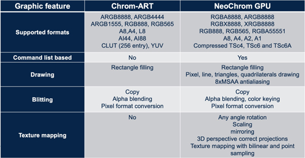
Comparing specs between Chrom-ART and NeoChrom
How Does NeoChrom GPU Integrate Into the TouchGFX Ecosystem?Historically, Chrom-ART represented one of ST’s first forays into graphical optimizations. Since then, we acquired TouchGFX and built an entire ecosystem with TouchGFX Designer, Simulator, and Generator. As a result, ST is integrating NeoChrom GPU into these tools right from the start. TouchGFX Designer contains demos showing a smooth animation running at 60 FPS on a circular display. More importantly, it shows the impact on the frame rate when NeoChrom GPU is off to help decision-makers grasp its importance. Similarly, the texture mapping widget will automatically use the new GPU if the MCU supports it. Hence, the immediate integration of the new IP within TouchGFX serves as a witness to ST’s cohesive ecosystem instead of a simple feature list.
From NeoChrom GPU to Real-World Performance What Are the Challenges to Graphical Performances?
The STM32U5
There exist two main challenges to graphical performances: an instructions-per-clock limitation and a memory issue. The first one often follows architectural innovations. Microcontrollers have ALU and FPU restrictions due to their size and low power consumption, but improvements in manufacturing processes allow for more transistors capable of handling more operations. NeoChrom GPU follows such trends with a hardware IP accelerating more types of graphical calculations. The second challenge is trickier but all the more critical because memory will always remain a scarce resource. While the STM32U599 will come with 2.5 MB of internal RAM capable of storing two frame buffers, many embedded systems need external RAM. The problem is that it comes with significant performance penalties.
What Are Unique STM32 Implementations?To solve this second challenge, NeoChrom GPU comes with hardware optimizations specific to STM32 MCUs. For instance, the STM32U5 relies on either an 8-bit Octal Serial Peripheral Interface (OSPI) or a 16-bit high-speed interface (HSPI) at 200 MHz to external memory modules to hasten fetching operations to the L2 cache. Similarly, the L1 cache can directly access two 832 KB frame buffers in the internal RAM. As a result, tessellation is significantly faster thanks to quick access to all the data necessary to render the image in real-time. Put simply, our engineers optimized performance by working on reducing the time it takes to access textures and other assets, ultimately accelerating rendering by up to six times.
What’s Next?The first industry feedback around NeoChrom GPU has been very positive. While many MCU makers have similar IPs to accelerate graphical computations, the specific STM32 optimizations and the TouchGFX ecosystem led many early alpha testers to adopt NeoChrom GPU instead of competing solutions. The new technology is already supported within TouchGFX 4.19, and a few alpha customers have already worked on production-ready UIs using an upcoming STM32U599 development kit. ST will also include NeoChrom GPU in other upcoming microcontrollers and we’ll update this blog post as they become public.
- Contact us to learn more about NeoChrom GPU
- Start a UI that will take advantage of NeoChrom GPU with TouchGFX Designer
- Check all the major features of the TouchGFX framework
The post NeoChromVG GPU, the 1st vector graphics accelerator for general-purpose MCUs enables single-chip designs appeared first on ELE Times.
Hand-held biosensor detects breast cancer biomarkers from saliva
I made a white HDD
 | submitted by /u/888Leander [link] [comments] |
The perfect multimeter doesn't exi...
 | submitted by /u/chataou [link] [comments] |
UK tech firms start commercial negotiations at SEMICON Korea
CSA Catapult’s achievements over 2018–2023 outlined in independent report
Indoor solar cells spur design-option reassessments

Conventional solar cells are just that: photovoltaic devices which, by their physics, extract and transform energy from the sun. Their sensitivity and efficiency are matched to the optical-energy spectrum of radiated and received power from the Sun to the extent possible, Figure 1.

Figure 1 The solar optical spectrum is complex and the available power per wavelength is a function of many factors. Source: Pennsylvania State University
In many small-scale applications, these same solar cells are used indoors and powered by ambient light from source’s overhead fixtures (which may be fluorescent or LEDs of various color temperatures), incandescent lamps (yes, some are still out there), diffuse or shaded natural light, and even specialized light such as halogen sources.
Given the indoor situation, two things are obvious:
- The designation as “solar” is somewhat of a misnomer since the Sun is no longer the source and so “photovoltaic” (PV) would be more accurate—but that’s the widely used, colloquial way of describing these cells.
- The energy spectrum of these indoor lighting sources is mismatched to the responsiveness of the solar cells, so efficiency is low.
While there have been some smaller, less-critical indoor products using solar power alone such as small calculators, such harvesting of ambient indoor optical energy is generally limited in its usefulness.
That situation may be changing as several companies have developed solar cells (we’ll stick with that misnomer) based on technologies which are very different from those used by conventional “real” solar cells. These indoor-optimized cells use complex layers of dyes along with specialized physical and chemical processes to achieve their indoor-optimized results.
Both Ambient Photonics (Scotts Valley, CA) and Exeger Operations AB (Stockholm) use variations of dye sensitized solar cell (shortened to DSC or DSSC) technology to produce light-sensitive cells which are optimized for indoor settings. The production process is a high-volume printing-like operation rather than the furnace-based process used for conventional solar cells.
Ambient says they have reinvented the chemistry of the dye sensitized solar cell (DSSC) with novel, proprietary molecules, using light-sensitive dyes to collect photons and convert them into electrons. In their electrochemical system, these light-sensitive dye molecules harvest and produce energy, with the dyes functioning similar to how chlorophyll behaves during photosynthesis in converting photons into energy.
They maintain that their energy-harvesting technology can harness photons across the light spectrum, yielding more than 90 percent conversion efficiency in low-light condition, even when compared to standard DSSC cells, Figure 2. They also function effectively despite the dynamic, changing indoor low-light conditions which are largely a function of the time of day.

Figure 2 Ambient says their DSSC process yields results which are superior to conventional film-based PV cells. Source: Ambient Photonics
Exeger’s dye sensitized solar cell uses a new architecture which they say improves real-life performance, provides greater flexibility, and offers seamless integration possibilities. In their approach, a unique conductive electrode material has replaced the traditional expensive and inefficient indium-tin-oxide (ITO) layer, Figure 3.

Figure 3 The Exeger’s process requires multiple layers of sophisticated materials and films and is compatible with mass production. Source: Exeger Operations AB
Dubbed Powerfoyle, it is flexible and durable and so can be integrated on curved surfaces such as headbands, Figure 4. It can be produced in sizes from 15 cm² to 500 cm², and therefore integrated into products ranging from small IoT sensors to speakers and larger accessories.

Figure 4 A bendable, flexible solar cell opens up new design-in and application opportunities. Source: Exeger Operations AB
For most design engineers, how these companies have achieved their indoor-friendly solar cells is not as important as what these innovations may do with respect to design options and degrees of freedom. Do power sources such as these enable increased consideration of IoT devices (sensors, trackers, shelf labels, and even remote controls) which do not need battery replacement, yet require more power other harvesting schemes (such as ambient RF-harvesting) support? For example, electronic door locks in hotels are an interesting possibility, as they are continually exposed to indoor lighting and used relatively infrequently; in theory, that’s a good combination of harvesting and use cycles.
Applications do not have to be limited to such small devices, either; Exeger has an agreement with a headphone manufacturer for ambient-powered units with the headband capturing ambient light. The same idea can be used for providing power to safety vests and alarm devices.
Of course, the energy source itself is only part of the harvesting chain. For designers, the dominant issue is not “how did they do it” but instead “what can it perhaps do for me?”; “what new opportunities does it provide?”; and “what do I need to do in my design to make use of this power source?”
For example, designers will have to decide on a suitable energy-storage and charging arrangement, whether using a rechargeable battery and the issues of limits on viable charge/discharge cycles, or a supercapacitor and the unique issues of using these non-chemical storage cells.
It will be interesting to see if these indoor-friendly solar cells become a standard part of the design-in possibilities, or if they have downsides which only become apparent when you get into the nitty-gritty design details of product design, manufacturing, use patterns, and long-term performance.
Do you see a viable energy-harvesting role for these non-Sun-driven solar cells? Would they allow you to create something you haven’t been able to do thus far? What possible design-in issues do you see?
Bill Schweber is an EE who has written three textbooks, hundreds of technical articles, opinion columns, and product features.
Related Content
- Keep solar panels clean from dust, fungus
- Are solar-powered cars the ultimate electric vehicles?
- Home solar-supply topologies illustrate tradeoff realities
- Enough With the Solar Power ‘Magic,’ Please!
- Solar Energy Harvesting: A Great Solution, Except When It’s Not
The post Indoor solar cells spur design-option reassessments appeared first on EDN.
BluGlass secures $4.3m via share placement, and launches share purchase plan offer to raise up to $9m
55MHz on breadboard. Built a Schmitt Trigger with discrete transistors to convert AC to TTL while prototyping a frequency counter on Arduino Nano.
 | submitted by /u/ChopSticksPlease [link] [comments] |
Bami Bastani appointed executive chairman of Sivers Semiconductors Inc
OIF showcasing interoperability at OFC with record 47 member companies
Lumentum’s quarterly revenue falls 27.5% to $366.8m
Will AI PCs be a new sweet spot for CPUs and DRAMs?

The personal computer (PC) industry is warming up to a new sweet spot: PCs incorporating artificial intelligence (AI) capabilities. Intel and Microsoft—the primary beneficiaries of the PC revolution—are now pushing PCs with AI-enabled CPUs and AI-powered software assistants, respectively, to move AI applications from the cloud to the PC realm.
In other words, AI PCs embedded with specialized chips can run AI models locally without relying on the cloud. That, according to Intel CEO Pat Gelsinger, will make AI services cheaper, faster, and more private than using services based in cloud-centric data centers. “You’re unleashing this power for every person, every use case, every location in the future,” he said at the CES 2024 in Las Vegas.
Intel, while competing with AI powerhouse Nvidia in server space, clearly sees an opportunity to catch up in its forte: PC processors. What it’s doing right now is integrating neural processor units (NPUs) into PC processors; NPUs are specialized semiconductors dedicated to handling AI tasks.
Intel’s Meteor Lake laptop CPU has incorporated an NPU to support third-party AI software features. Its archrival in the PC hardware space, AMD, has also been shipping AI PC processors. Next, Nvidia showcased three new GPUs—RTX 4060 Super, RTX 4070 Ti Super, and RTX 4080 Super—for AI-ready laptops at a virtual event before CES 2024.

Figure 1 Meteor Lake CPU has incorporated an NPU to support AI applications. Source: Intel
Besides AI-ready processors, memory chipmakers like Micron, Samsung, and SK hynix are also eyeing AI PCs to enable AI accelerators to run powerful assistants on personal computers. New laptops currently come with as much as 8 MB of RAM, and it’s likely to double in Windows-based AI PCs. In fact, a large language model (LLM) running an AI assistant could require more than 16 MB of memory.
Take the example of the Llama 2 family of AI models created by Meta, which requires nearly 30 GB of RAM for its modest variant. Moreover, the amount of memory in AI PCs will likely increase with the availability of more powerful AI accelerators and processors.

Figure 2 Copilot AI assistant is built around OpenAI’s GPT-4 model. Source: Microsoft
At the moment, consumers are only warming up to AI personal computers, and it’ll take a while before more native applications are made available for AI PCs. However, both hardware and software for AI PCs will become more powerful over time, and that’s good news for semiconductor devices like CPUs, GPUs, and DRAMs.
Related Content
- Getting a Grasp on AI at the Edge
- Navigating the Good, the Bad, the Ugly of AI
- AI chat tool for PCBs aims to simplify hardware design
- Democratizing Edge AI and ML with a No Code Approach
- Edge AI vs. Cloud AI: What’s Best for Sustainable Computing Systems?
The post Will AI PCs be a new sweet spot for CPUs and DRAMs? appeared first on EDN.
Oscilloscope persistence displays

Persistence displays retain waveform traces on the screen, allowing them to decay over a user set time duration, they allow users to see a history of signal variations on the screen. This feature is very useful if you are adjusting a signal, as it allows you to see the changes as they are made. Some oscilloscope applications require displaying a history of events in order to see how the signal varies over time. Persistence displays are key tools for viewing such signal changes as a function of time over multiple acquisitions. The most common applications that use persistence displays include jitter analysis of a serial data transmission and eye diagrams used for digital communications systems (Figure 1).

Figure 1 The persistence display of timing jitter on an edge. Multiple acquisitions are retained on the display of the edge to show the variation in its timing. Source Arthur Pini
This is an analog persistence view of jitter on a clock edge, it is a monochrome display where the brighter areas are the more often occurring signal paths and the duller areas occur less often. The center area of the transition is brighter, meaning more edges pass at that time than during the times corresponding to the outer edges.
The same data can be viewed in color-graded persistence, a tool used to map the frequency of occurrence spectrally. Most frequent events appear in red while the least frequent events are shown in violet (Figure 2).

Figure 2 A color graded persistence display of the same edge jitter. The red areas occur more often than violet areas. Source Arthur Pini
The intermediate frequency of occurrence is mapped spectrally, from most to least often occurring as red-orange-yellow-green-blue-indigo-violet.
Multiple acquisitions are acquired and stored in a persistence map which shows signal variations over time. The persistence decay time is user-selectable with a time constant from half a second to infinite. A saturation control allows users to control the mapping of frequency of occurrence to intensity or color.
Eye and state transition diagrams
Persistence displays also help analyze data communications signals, where they are used to display eye diagrams and state transition diagrams (Figure 3).

Figure 3 The eye diagrams of the I and Q components and state transition diagrams of a 16-QAM signal rendered in monochrome analog persistence. Source: Arthur Pini
The eye diagrams of a 16-QAM signal show the results of 12,890 acquisitions of the I and Q signal components, which are also cross plotted as an X-Y plot, forming the state transition diagram shown in the upper right corner. Again, the intensity variations are proportional to the amount of time a waveform falls on a particular point on the display. The highly repetitive elements of a signal are brighter than the rarely occurring signal events. The data states, which appear as horizontal lines in the I and Q traces, are written more often and show up brighter than the transitions, which take different paths and occur with less frequency at any given point. The same is true of the state transition diagram where the data states appear as bright dots and the transition paths have a lower intensity.
Persistence histograms
All the data behind the persistence display is available and can be used to quantify the acquired data statistically. One example is to generate a histogram from the persistence display. The oscilloscope used in this article has a function called persistence histogram, it lets the user define either a horizontal or vertical slice through the
persistence display and then forms a histogram as shown in Figure 4.

Figure 4 A persistence histogram with a horizontal slice of the jitter persistence display centered at a level of 0 mV with a width of 10 mV. Source: Arthur Pini
The persistence histogram appears in the trace below the persistence display. Cursors are used to mark the location where the histogram slice originates. In a vertical slice, each bin of the histogram contains a class of related amplitude levels. A horizontal slice, used in the example, produces a histogram where each bin contains a class of related time values.
In the example, the vertical axis of the histogram reads the number of times a specific horizontal pixel is hit. The peak of the histogram corresponds to the central area with a light blue color, while the falling sides correspond to the persistence display changing from indigo to violet. The histogram can be measured using the oscilloscope’s measurement parameters, the measurement parameters P1 through P3 beneath the display grids read the mean, the standard deviation, and the range of the histogram. Parameter help markers annotate the locations of these measurements on the histogram itself.
Persistence histograms can also be applied to eye diagrams showing the horizontal timing uncertainty as well as the vertical deviation (Figure 5).

Figure 5 Application of persistence histogram to an eye diagram permits analysis of noise and jitter on the eye. Source: Arthur Pini
The histogram in the center trace was taken from a horizontal slice through the eye crossing and shows the range of variation in the time of the crossings. The lower histogram was taken using a vertical slice centered between the crossings, it shows the uncertainty in the amplitude of the eye in the center. Some oscilloscopes may not offer measurements that quantify eye characteristics such as eye height and width, .these can actually be obtained using persistence histograms and their associated statistical measurements.
Persistence trace functions
Persistence trace functions take the histogram of the persistence values over a number of vertical slices set by the user and extract the mean, standard deviation, and range of the persistence data at each slice. It then plots the extracted statistical parameter over time (Figure 6).

Figure 6 Examples of the persistence trace mean (second from the top), persistence trace sigma (third from the top), and persistence trace range (bottom) traces. Source: Arthur Pin)
The persistence trace mean function plots the mean value of the histograms at each of the user’s selected intervals. The resultant plot is the average value of the source persistence trace. In this example, the trace is taken from one thousand points along the persistence trace. This function shows the underlying waveform without vertical noise. Persistence trace sigma plots the minimum and maximum values of the standard deviation about the mean using an extrema plot. The plot shows mean + and – one standard deviation. This function provides a view of the rms noise on the source waveform. The persistence trace range plots the minimum and maximum values of the persistence histogram about the mean and shows the range of the histogram. It is the worst-case range of possible values, especially noise, at each point.
Persistence trace mean is the most useful of the functions allowing a quick determination of the average value of a persistence trace. It is also useful to smooth out traces acquired with low sample point counts (Figure 7).

Figure 7 The persistence trace mean shows all the possible states in waveform with a low sample count by retaining multiple acquisitions. Source: Arthur Pini
Waveforms with low sample counts, displayed with linear interpolation, may appear angular and discontinuous however they are not, and over multiple acquisitions, they trace a smooth waveform. Using persistence trace mean to view the waveform allows the persistence history to fill in the intermediate states and smooth the waveform, showing its actual structure.
3-D persistence display
Adding vertical height to a persistence display proportional to the rate of occurrence gives you a three-dimensional (3-D) effect. This 3-D persistence display creates a topographical view of your waveform.
As shown in Figure 8, this is most useful when studying X-Y plots of signals such as QPSK.

Figure 8 The in-phase and quadrature components of a QSPK signal and a three-dimensional persistence plot of a QPSK state transition diagram. Source: Arthur Pini
The three-dimensional plot retains the color or intensity coding of the persistence displays but adds height proportional to the frequency of occurrence of the display pixels. The shape of these peaks provides an alternative view of the frequency of occurrences in your signals. In this example, the data states of the signal which occur most frequently appear as the highest elements in the X-Y display and are coded in red. Transition paths have more variation and occur less repetitively. They are lower on the display and coded in yellow/green. Off path regions are at the bottom of the display, coded in violet. Controls allow for rotating the 3-D plot to view it from different angles.
The 3-D display can be rendered in three different qualities. The first is as a solid, as is shown, and is the default quality. It can also be rendered in the wireframe quality; this is constructed using lines of equal intensity to create the persistence map. The third quality is shaded, which is only available in monochrome persistence. Shaded quality shows the 3-D object as if it were illuminated by projected light, the shading emphasizes the shape of the object.
The value of persistence displays
Whether used to measure jitter, eye diagrams, or state transition diagrams, persistence is a valuable display technique. When combined with math persistence analysis tools and related measurements, it becomes a powerful tool for quantifying signal variations.
Arthur Pini is a technical support specialist and electrical engineer with over 50 years of experience in electronics test and measurement.
Related Content
- Using oscilloscope X-Y displays
- 10 More tricks to extend oscilloscope usefulness
- Digital oscilloscopes: When things go wrong
- Closing the gaps in your digital oscilloscope waveforms
The post Oscilloscope persistence displays appeared first on EDN.
What You Need to Know About Chip Resistors
Wondering what chip resistors are? Then you are in luck because this article will answer that question in detail. Not only that, but we’ll also reveal how they are made, how they work, and the types of technology these devices use. There’s a lot to cover, so let’s get started.
Chip resistors aka surface mount devices (SMDs) are integrated circuit devices. They are either rectangular or square. These Resistors are designed to resist the flow of electric current. They are used to regulate, safeguard, and operate circuits.
SMDs can be found in all kinds of sizes. Some are too tiny to pick up with your hands. Values such as E192 and E3 are common values you can readily find.
Surface mount devices are found in most electronic products with advanced circuitry. SMDs are known as such because they are placed directly on the electronic product’s printer circuit board. Without these resistors, there’ll be nothing regulating the current flow within the product. In such a case, the electronic product is subject to damage that can destroy it.
How They Are MadeTo manufacture a chip resistor, the end connection of electrode bases is attached to the substrate of a ceramic material. To ensure that the attachment is firm, the resistor is fired. The next step is the printing or depositing of the film of a resistive material. Again, the resistor is fired.
Afterward, several layers of protective coat are used to cover the resistor. You can click here to find out more about the protective coating. Before the application of the next coat, the previous one is allowed to dry first.
The addition of these protective coatings is beneficial to the SMD and the electronic product. First of all, the protective coating protects the resistor from mechanical damage. Secondly, it prevents contaminants and moisture from affecting these devices.
Chip resistors with large surfaces are designed with a marking. When packaged these devices resemble blister rolls. They can then be used on pick-and-place electronic machines.
How They WorkChip resistors are designed to restrict the flow of circuit current. These chip resistors sometimes are designed with a definite resistance value. This type is known as a fixed resistor.
On the other hand, the resistance value of the second group isn’t definite but is designed to operate within a range. This type is known as a variable resistor or potentiometer. Because of its passive function, a resistor only decreases voltage or current signals.
The perfect resistor is linear. In this case, the instantaneous current that passes through the SMD is proportional to the instantaneous voltage being applied. Resistors that do not operate linearly include varistors and thermistors.
In electronic circuits, these SMDs are formed into several series based on resistance value and power. Surface mount devices act as voltage dividers and shunts to control and steady voltage and current in circuits. You can visit https://eepower.com/ to learn more about shunts in circuits. They also serve as circuit-matching loads.
 Chip Resistor Technology
Manufacturers can choose from different technologies when manufacturing an SMD. These different technologies have their advantages and disadvantages. The following are the most commonly used chip resistor technologies:
Thin FilmChip resistors manufactured with this technology are made by depositing a thin metallic coating on the upper part of a ceramic substrate. Due to this design, these devices have greater resistance for a certain area. As such, they are economical and space-efficient.
The downside is that they are prone to failure. The reason for this is that they can easily heat up or be affected by water vapor. Chemical contamination is another reason that can lead to the failure of these SMDs.
Thick FilmThese are made by applying the paste of a restive metal onto a base. Because of this, the resistance they provide for a certain area is usually high. Furthermore, they are cheaper when you compare them to other resistor types such as wire-wound resistors.
The disadvantage of using this technology is it produces more noise compared to thin-film resistors. Although they have similar frequency response to thin films, they are still noisy. Despite this, they are still very used in circuit units that don’t require durability and accuracy.
FoilThis technology involves the use of a metallic foil applied to a ceramic substrate. It is then photo-etched via a restive pattern. The result is a resistor with enhanced stability, low capacitance, reduced noise, and non-inductance. All these benefits are achieved without losing precision and speed. As such, these surface mount devices are in high demand.
Reading a Chip Resistor CodeThese devices are usually marked with a code known as SMD Resistor Codes. The code might be made of three or four digits. The purpose of this code is to reveal the device’s resistance value.
To interpret a code with three digits, take the first two digits as a standalone number and the third digit as a standalone number. The first two digits are the significant resistance number while the third digit is the multiplier. You use the third digit to multiply the first two to get the resistance value.
For a code with four digits, take the first three digits as a standalone number and the fourth digit as a standalone number. The first three digits are the significant resistance number while the fourth digit is the multiplier. You use the fourth digit to multiply the first three to get the resistance value.
Chip Resistor AdvantagesThey do not take up much space in a product. Having several connections for every single component is proof of their high component density. Also, they have a simpler automated assembly and are much faster.
Because of their structured design, the PCB has fewer holes bored into it. You can visit https://www.techtarget.com/ to learn more about the Printer Circuit Board. Also, they can be on either side of the PCB. Their mechanical performance is enhanced, and they have cheap parts.
Chip Resistor DisadvantagesTheir solder components can be prone to damage which happens via thermal cycling that moves potted compounds. Also, the component packages they are designed with prevent them from being installed into sockets. Furthermore, when there is a need for reassembling or repair, an expert must handle it and extensive tools are required.
ConclusionIn this article, we’ve discussed what you need to know about chip resistors. We discussed what they are, how they are made, how they work, and the technologies used in making them. We also revealed the advantages and disadvantages of these devices.
The post What You Need to Know About Chip Resistors appeared first on Electronics Lovers ~ Technology We Love.
EEVblog 1598 - ANENG AC11 Socket Tester TEARDOWN + SCHEMATIC Reverse Eng
Solved once and for all.
 | submitted by /u/1Davide [link] [comments] |
May car is powered by a MOS 6502
 | submitted by /u/twiggs462 [link] [comments] |
Weekly discussion, complaint, and rant thread
Open to anything, including discussions, complaints, and rants.
Sub rules do not apply, so don't bother reporting incivility, off-topic, or spam.
Reddit-wide rules do apply.
To see the newest posts, sort the comments by "new" (instead of "best" or "top").
[link] [comments]
Rx Tx routing woes be gone!
 | Put away the scalpel and wire wrap wire. [link] [comments] |
Сторінки


![[link]](https://i.redd.it/dmepj5shneic1.jpeg)
![[link]](https://i.redd.it/1mskgnzozyhc1.jpeg)
![[link]](https://i.redd.it/13nk1asa5vhc1.jpeg)
![[link]](https://i.redd.it/reic232k6qhc1.jpeg)