
Збирач потоків
A crash course in 3D IC technology

What’s 3D IC, and what’s causing the shift from 2D IC to 3D IC? How does this new technology relate to heterogeneous integration and advanced packaging? What is required for a successful 3D IC implementation? EDN recently published a three-article series to cover multiple facets of this advanced packaging technology.
Below is a sneak peek at this three-article series, which explains 3D IC fundamentals, microarchitectures, toolkits, and design use cases.
Part one, titled “Making your architecture ready for 3D IC”, provided essential context and technical depth for design engineers working toward highly integrated, efficient, and resilient 3D IC systems. It explains 3D IC microarchitectures that redefine how data and controls move through a system, how blocks are partitioned and co-optimized across both horizontal and vertical domains, and how early-stage design decisions address the unique challenges of 3D integration.
Making your architecture ready for 3D IC
Part two, titled “Putting 3D IC to work for you”, outlines the challenges and opportunities in adopting 3D IC technology. It demonstrates how 3D IC enables efficient chiplet integration and reuse, accelerates innovation, and guarantees manufacturability across organizational boundaries. The article also provides a detailed examination of 3D IC design toolkits and workflows, as well as their incorporation of AI technology.
The third and final part, titled “Automating FOWLP design: A comprehensive framework for next-generation integration”, presents fan-out wafer-level packaging (FOWLP) as a case study, showing how automation frameworks manage the inherent complexity of advanced packaging and the scale of modern layouts, racking up millions of pins and tens of thousands of nets. It also demonstrates how effective frameworks promote collaboration among package designers, layout specialists, signal and power integrity analysts, and thermal and mechanical engineers.
Automating FOWLP design: A comprehensive framework for next-generation integration
Related Content
- 3D IC Design
- Thermal analysis tool aims to reinvigorate 3D-IC design
- Heterogeneous Integration and the Evolution of IC Packaging
- Tighter Integration Between Process Technologies and Packaging
- Advanced IC Packaging: The Roadmap to 3D IC Semiconductor Scaling
The post A crash course in 3D IC technology appeared first on EDN.
CEA-Leti and CRHEA present step toward full-color AR/VR micro-displays at MicroLED Connect Conference
✅ Оголошується конкурс на заміщення посад
Національний технічний університет України "Київський політехнічний інститут імені Ігоря Сікорського" оголошує конкурс на заміщення вакантних посад. Термін подання документів до 26.10.2025 року.
Конкурс на заміщення вакантної посади завідувача кафедри
Конкурс на заміщення вакантних посад професорів
Конкурс на заміщення вакантних посад доцентів, викладачів
Photon Design exhibiting product range at ECOC 2025
Socomec Launches COUNTIS P new range of Smart AC/DC Energy Meters for Efficient Energy Management
From design to commissioning, Socomec guarantees high-performance, sustainable electrical installations
Socomec announced the launch of its latest innovation: COUNTIS P, a next-generation range of smart energy meters designed to meet the evolving needs of modern infrastructure. With over three decades of industry expertise, this launch reinforces Socomec’s commitment to innovation, sustainability, and excellence in energy efficiency and digital transformation.
Mr. Meenu Singhal, Regional Managing Director – Greater India, Socomec Innovative Power Solutions, emphasized the significance of the launch, stating, “As the energy consumption becomes increasingly complex across sectors, organizations are under pressure to manage usage more efficiently while ensuring compliance and sustainability. COUNTIS P offers a smarter, simpler way to manage energy through its compact design, AC/DC compatibility, and seamless integration with digital platforms. It empowers businesses to gain real-time insights, improve cost allocation, and drive meaningful progress toward energy efficiency goals”. He stated that this innovation demonstrates Socomec’s ongoing efforts to deliver intelligent, sustainable solutions that support customers in navigating today’s energy challenges while preparing for tomorrow’s opportunities.
The COUNTIS P range delivers precision metering, modular design, and advanced connectivity, including Modbus RTU/TCP protocols. Designed for versatility, COUNTIS P is compatible with both AC and DC systems and operates seamlessly across single-phase and complex three-phase networks. Built to perform in harsh environments, it maintains high accuracy even under extreme temperature conditions. Its plug-and-play QuickConnect installation simplifies deployment, reducing time and complexity for installers and integrators.
When integrated with Socomec’s digital monitoring platforms, COUNTIS P provides real-time energy insights that help customers track consumption, identify inefficiencies, make data-driven decisions, reduce operational costs, and support their sustainability goals. These capabilities make COUNTIS P a future-ready solution for organizations looking to optimize energy use and meet tightening regulatory standards.
In many sectors, managing sub-billing remains a critical challenge. Accurate sub-metering enables fair and transparent rebilling of energy consumption across tenants or business units. COUNTIS P meters are MID-certified, ensuring reliable accuracy and full compliance with regulatory requirements. This makes them an ideal solution for organizations seeking to avoid billing errors and ensure transparency in energy cost allocation. With features like QuickConnect technology, AC/DC compatibility, and MID certification, COUNTIS P is ideal for buildings, industry, infrastructure, and EV charging stations.
Socomec supports its customers throughout the entire lifecycle — from design to commissioning — ensuring high-performance, compliant, and sustainable electrical installations. As energy consumption becomes a critical issue for businesses, reducing kilowatt-hour usage not only lowers costs but also minimizes environmental impact. In this context, COUNTIS P stands out as a smart, reliable, and efficient tool for modern energy management.
The post Socomec Launches COUNTIS P new range of Smart AC/DC Energy Meters for Efficient Energy Management appeared first on ELE Times.
Setting Up PCM and I2S Formats for Reliable SCO Loopback Transmission
In the contemporary wireless audio industry, providing crystal-clear uninterrupted sound is such a major and recurrently faced problem. Depending on the nature of Bluetooth headsets ethereally connecting with other apparatus modules over wireless ambience or in the car for in-roads communication purposes, or in gaming devices, it is imperative that, from the engineers’ standpoint, audio signals need to stay unstuck from distortion. To validate and optimize further, SCO (Synchronous Connection-Oriented) loopback transmissions can be put to use.
In this manual, loopback mode is described. Why do we need loopback testing in Bluetooth audio? And how does one configure PCM or I2S for an SCO loopback using the Infineon AIROC Bluetooth controllers?
What is a Loopback Mode?
Loopback mode is a constraint and verification method for wireless audio. Rather than train the audio signal back to a set destination (e.g., speakers, headphones, etc.), the signal is looped back to the originating source. This allows the developers to check the signal quality, such as verifying hardware configurations and troubleshooting towards identifying any mismatch, without dependence on external devices for tests.
Normal vs. Loopback Mode:
Normal Mode: Audio is transmitted to the output device.
Loopback Mode: Audio is redirected back to the source for testing.
Test Environment
To configure SCO loopback transmission, you’ll need:
AIROC CYW20706 headset demo (PCM_OUT source) → GitHub demo project
Linux mbt tool for HCI command input → GitHub mbt tool
AIROC CYW89072 (or any supported Infineon Bluetooth controller) with firmware
Step-by-Step Setup for SCO Loopback Transmission
Step 1: Program the CYW20706 and Bring Up the Demo
- Flash the CYW20706 using ModusToolbox.
- Use the client control tool to run the demo.
- Pair a phone with the CYW20706 and start playback.
Step 2: Connect Hardware
Wire the CYW20706 PCM_OUT pin to the CYW89072 PCM_IN pin.
Step 3: Download Firmware
./mbt download [filename].hcd –minidriver
Step 4: Enable Loopback Mode
./mbt input_command 24fc0101
PCM Configuration
8K PCM
./mbt input_command 1cfc050001000101
./mbt input_command 24fc0101
16K PCM
./mbt input_command 7efc03010200
./mbt input_command 6dfc0400010102
./mbt input_command 1cfc050002000101
./mbt input_command 1efc050000030000
./mbt input_command 24fc0101
I2S Configuration
8K I2S
./mbt input_command 7efc03000200
./mbt input_command 6dfc0401010001
./mbt input_command 24fc0101
16K I2S
./mbt input_command 7efc03010200
./mbt input_command 6dfc0401010102
./mbt input_command 24fc0101
Pin Configuration Notes
For controllers like CYW555xx or CYW43xx, an additional command may be required to route PCM/I2S to default pins:
./mbt input_command 61fc0501b9b8b8b8
By default, the setup assumes TDM2 pins are in use. If you are using alternative pins, adjust the commands accordingly.
Key Takeaway
SCO loopback transmission is an invaluable tool for validating wireless audio performance. By configuring PCM or I2S formats with Infineon’s AIROC Bluetooth controllers, engineers can easily verify signal integrity, fine-tune system performance, and ensure a smooth end-user audio experience.
(This article has been adapted and modified from content on Infineon Technologies.)
The post Setting Up PCM and I2S Formats for Reliable SCO Loopback Transmission appeared first on ELE Times.
Looking Into What Makes Glasses Smart: A Guide to the Flexible PCBs in Smart Glasses
As emerging glasses and systems bring the virtual and physical worlds closer together than ever before, making navigation, entertainment, and even gaming way easier and more exciting, it is the power of electronics that makes it happen. In such a scenario, let’s examine the technology that makes it possible, seamless, and modern. As we move into the topic, it’s essential to emphasize that the PCB is the most crucial central platform that connects and organizes all the electronic components in a smart glass or an AR/VR device.
What type of PCB is used in Smart Glasses?
Due to the need for flexibility, adaptability, and reliability, the majority of smart glasses today are manufactured using Flexible Printed Circuit Boards (FPCBs). These are thin, lightweight circuit boards made from pliable materials that bend easily without breaking. As opposed to the rigid circuit boards, FPCBs are made with the intent to empower technology with convenience.
What makes FPCBs the go-to Choice?
PCBs enable engineers to redefine electronics with unique shapes. As it can withstand repeated bending cycles, by default, it becomes an ideal choice for compact and curved designs of smart glasses or AR/VR gear. It is a prime example of how technology integrated with aesthetics and need can empower a whole segment of innovation and seamlessness.
Smart Glasses and FPCBs are a match made in heaven, as FPCBs not only constitute the central platform, which is what a PCB usually does, but also enable the engineers to render various specific characteristics of glasses into the segment of Smart Glasses.
Electrical yet Appealing & Convenient: Secrets
To make a device fitted with so many components, yet maintain it for optimal use as a glass, necessitates a plethora of considerations to be ticked. This takes us to the next part of our story, which is the types of FPCBs depending on the materials it is made of. These materials render significant properties to the FPCBs, enabling them to not only facilitate technology but also combat its ills.
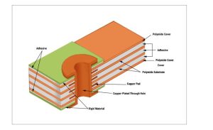 Structure of an FPCB
Primary materials used in these applications are:
- Polyimide (PI): The most commonly used substrate for flexible PCBs, polyimide offers outstanding thermal stability (up to 400 °C) and high mechanical strength. It can withstand thousands of bending cycles, making it ideal for the constantly moving and compact environment of smart eyewear.
- Polyester (PET): A more economical alternative to polyimide, PET provides decent flexibility but is less durable. It works best in static or low-bend applications, and is often chosen for simpler or less demanding wearable designs.
- Copper Foil: Copper is the standard conductor in flexible PCBs. Among the types, rolled-annealed (RA) copper is preferred over electrodeposited (ED) copper because of its superior flexibility and fatigue resistance—key for handling repeated bends in devices like smart glasses.
- Adhesives and Coverlays: Adhesives secure the layers of a flexible PCB, while coverlays (thin protective films) safeguard the circuitry. Both must retain flexibility and adhesion under stress to prevent issues like delamination during everyday use.
Engineers frequently favor polyimide-based substrates for their durability, particularly in premium AR glasses where long-term reliability is essential. Beyond strength, the choice of material also influences signal performance—polyimide’s low dielectric loss makes it well-suited for high-frequency applications such as 5G connectivity in smart devices.
Design Considerations with FPCBs
Since smart glasses can be subjected to repeated bending and need proper signals to enable their proper usage, it is important to design them accordingly to suit future needs. In engineering terms following considerations rank the highest:
Bending Radius:
- Maintain ≥10× PCB thickness for dynamic bends, ≥3× for static.
- Example: 0.1 mm PCB → 1 mm minimum dynamic bend radius.
Trace Layout & Spacing:
- Route traces perpendicular to bend lines.
- Avoid vias/components in bend zones.
- Keep ≥0.1 mm spacing to prevent shorts during flexing.
Tear-Drop Pads:
- Use tear-drop geometry at trace–pad junctions to minimize stress concentration and cracking.
Layer Stack-Up:
- Use symmetrical stack-ups to keep the neutral axis centered.
- Reduces stress on multilayer FPCs, especially in curved frame designs.
In AR glasses, an FPC can route signals from the microdisplay in the lens to the control unit in the frame, flexing around corners without adding bulk. This ability to combine compact routing with mechanical flexibility makes FPCs fundamental to wearable design.
Is it all Always Good with FPCBs?
To give a straight answer, no. Neither is the case with any technology in the world. Let’s look into certain challenges that FPCBs have to offer when it comes to Smart Glasses:
- Maintaining Signal Integrity: With FPCBs having thin dielectric layers, high-frequency signals for wireless connectivity can face significant challenges. To counter this, manufacturers often turn towards low-loss materials like modified polyimide and ensure precise impedance control, targeting values like 50 ohms for optimal performance.
- Ensuring Bend Durability: Repeated flexing can fatigue copper traces. Mitigation strategies include using rolled-annealed (RA) copper and reinforcing bend zones with stiffeners or extra coverlay layers to better distribute mechanical stress.
- Miniaturization: Smart eyewear requires ultra-compact PCBs with high-density interconnects. Techniques like laser-drilled microvias (as small as 0.05 mm) enable dense, high-performance circuit layouts.
By leveraging these methods, manufacturers can deliver flexible PCBs that meet the strict demands of smart eyewear—combining durability, miniaturization, and high-speed signal integrity where Flexible PCBs are central to smart eyewear, enabling sleek, lightweight designs. Success depends on material choice, proper bend-radius design, and precise rigid-flex assembly—key factors for building reliable, innovative wearables
The post Looking Into What Makes Glasses Smart: A Guide to the Flexible PCBs in Smart Glasses appeared first on ELE Times.
For more secure AI and ML models: Infineon’s OPTIGA Trust M backs Thistle Technologies’ Secure Edge AI solution
Infineon Technologies AG provides its OPTIGA Trust M security solution to Thistle Technologies for its new cryptographic protection for on-device AI models to its security software platform for embedded computing products based on the Linux operating system (OS) or on a microcontroller. The new capabilities in the Thistle Security Platform for Devices, along with Infineon OPTIGA Trust M security solution as tamper-resistant hardware-based root-of-trust, protect the valuable intellectual property (IP) in the AI models deployed in edge AI applications, and in the training data sets on which they are based.
The Thistle Security Platform for Devices that includes the Infineon OPTIGA Trust M security solution, provides ready-made, cloud-managed security components which integrate seamlessly into Linux OS-based devices and microcontrollers. Instead of building and maintaining a one-off cybersecurity stack, OEMs can deploy a proven, continuously updated foundation in hours, and scale it across large, heterogeneous fleets of devices. The Security Platform enables both secured boot and over-the-air (OTA) updating, and is compatible with a broad range of microprocessors, systems-on-chip (SoCs) and microcontrollers. Infineon OPTIGA Trust M security controller enables secured key provisioning, tamper-resistant key storage, and efficient cryptographic operations for encryption and decryption, taking care that only trusted, authenticated, and verified AI models are deployed in edge AI applications.
Thistle has extended its solution to include built-in protection for on-device AI models and data, using cryptographic keys stored in Infineon’s tamper-resistant security controllers, OPTIGA Trust M. The three key features of the new Thistle Secure Edge AI solution are:
- Hardware-backed model encryption – AI model encryption key is secured by OPTIGA Trust M security solution. Each device has a unique AES 256-bit key securely stored in OPTIGA Trust M, which is used to secure the AI Model encryption key. This means that the AES key is used for encryption and decryption inside the OPTIGA Trust M only. Even if a device is lost, decommissioned, or disassembled, the manufacturer’s IP embedded in the model is still efficiently protected. At launch, this feature is enabled on the Infineon OPTIGA Trust M security solution.
- Secured model provenance – in OTA updates, the Thistle platform enables cryptographically signed, tamper-evident delivery of AI models and firmware directly from the training platform to the device, taking care that every installed instance of a model can be traced and verified.
- Signed data and data lineage – device-generated or collected data can be signed on-device and tagged with provenance metadata. This means that downstream systems which might use the data to train or refine AI models can check the provenance of the data, and of the version of the model that the device was running when it generated the data.
Animesh Ranjan, Head of Partnerships & Ecosystem at Infineon says: “At Infineon, we are pleased to expand our collaboration with Thistle Technologies to deliver stronger protection for AI models running at the edge. By combining the OPTIGA Trust M security solution with the Thistle Security Platform, we enable device makers to safeguard their AI with hardware-anchored security that is both practical and scalable.”
Window Snyder, Chief Executive Officer of Thistle Technologies, says: “It is always our goal to make robust security capabilities accessible for device makers. With Infineon’s OPTIGA Trust M and the Thistle Security Platform, manufacturers can protect AI models and data with proven cryptography and deploy at scale quickly. Together we give customers a straightforward way to ship devices that can securely verify, encrypt, and update AI models.”
The post For more secure AI and ML models: Infineon’s OPTIGA Trust M backs Thistle Technologies’ Secure Edge AI solution appeared first on ELE Times.
New Investments Flowing Into Photonics—Part 1: Trends Pointing Upwards
I'm in love with this build123d + KiCad workflow for parametric CAD
This parametric case is described in <150L of Python and it loads the board edge and footprint positions straight from the KiCad PCB file. In the video I also load the exported KiCad STEP 3d model just for visual inspection. Source here for the curious.
[link] [comments]
🏆 МОН оголошує конкурс наукових проєктів молодих учених!

📢 Міністерство освіти і науки України своїм наказом від 16.09.2025 №1253 17 вересня 2025 року оголосило конкурсний відбір проєктів фундаментальних наукових досліджень, прикладних наукових досліджень та науково-технічних (експериментальних) розробок молодих учених, які працюють (навчаються) у зак
🚀 Реєстрація на найбільший у світі космічний хакатон NASA Space Apps Challenge

🚀 КПІшники, реєструйтеся на найбільший у світі космічний хакатон NASA Space Apps Challenge, який щороку проходить під егідою NASA у різних державах.
Протягом 48 годин команди вирішують практичні завдання. Цьогоріч їх 19!
Optical Chip Beats Counterparts in AI Power Efficiency 100 Fold
Meta Connect 2025: VR still underwhelms; will smart glasses alternatively thrive?

For at least as long as Meta’s been selling conventional “smart” glasses (with partner EssilorLuxottica, whose eyewear brands include the well-known Oakley and Ray-Ban), rumors suggested that the two companies would sooner or later augment them with lens-integrated displays. The idea wasn’t far-fetched; after all, Google Glass had one (standalone, in this case) way back in early 2013:

Meta founder and CEO Mark Zuckerberg poured fuel on the rumor fire when, last September, he demoed the company’s chunky but impressive Orion prototype:

And when Meta briefly, “accidentally” (call me skeptical, but I always wonder how much of a corporate mess-up versus an intentional leak these situations often really are) published a promo clip for (among other things) a display-inclusive variant of its Meta Ray-Ban AI glasses last week, we pretty much already had our confirmation ahead of the last-Wednesday evening keynote, in the middle of the 2025 edition of the company’s yearly Connect conference:
Yes, dear readers, as of this year, I’ve added yet another (at least) periodic tech-company event to my ongoing coverage suite, as various companies’ technology and product announcements align ever more closely with my editorial “beat” and associated readers’ interests.
But before I dive fully into those revolutionary display-inclusive smart glasses details, and in the spirit of crawling-before-walking-before-running (and hopefully not stumbling at any point), I’ll begin with the more modest evolutionary news that also broke at (and ahead of) Connect 2025.
Smart glasses get sportyWithin the midst of my pseudo-teardown of a transparent set of Meta Ray-Ban AI Glasses published earlier this summer:
![]()
I summarized the company’s smart glasses product-announcement cadence up to that point. The first-generation Stories introduced in September 2020:

was, I wrote, “fundamentally a content capture and playback device (plus a fancy Bluetooth headset to a wirelessly tethered smartphone), containing an integrated still and video camera, stereo speakers, and a three-microphone (for ambient noise suppression purposes) array.”
The second-generation AI Glasses unveil was led three-plus years later in October 2023, which I own—two sets of, in fact, both Transitions-lens equipped:

make advancements on these fundamental fronts…They’re also now moisture (albeit not dust) resistant, with an IPX4 rating, for example. But the key advancement, at least to this “tech-head”, is their revolutionary AI-powered “smarts” (therefore the product name), enabled by the combo of Qualcomm’s Snapdragon AR1 Gen 1, Meta’s deep learning models running both resident and in the “cloud”, and speedy bidirectional glasses/cloud connectivity. AI features include real-time language Live Translation plus AI View, which visually identifies and audibly provides additional information about objects around the wearer.
And back in June (when published, written early May), I was already teasing what was to come:
Next-gen glasses due later this year will supposedly also integrate diminutive displays.
More recently, on June 20 (just three days before my earlier coverage had appeared in EDN, in fact), Meta and EssilorLuxottica released the sports-styled, Oakley-branded HTSN new member of the AI Glasses product line:
The battery life was nearly 2x longer: up eight hours under typical use, and 19 hours in standby. They charged up to 50% in only 20 minutes. The battery case now delivered up to 48 operating hours’ worth of charging capacity, versus 36 previously. The camera, still located in the left endpiece, now captured up to 3K resolution video (albeit the same 12 Mpixel still images as previously). And the price tag was also boosted: $499 for the initial limited-edition version, followed by more mainstream $399 variants.
A precursor retrofit and sports-tailored expansionFast forward to last week, and the most modest news coming from the partnership is that the Oakley HTSN enhancements have been retrofitted to the Ray-Ban styles, with one further improvement: 1080p video can now be captured at up to 60 fps in the Gen 2 versions. Cosmetically, they look unchanged from the Gen 1 precursors. And speaking of looks, trust me when I tell you that I don’t look nearly as cool as any of these folks do when donning them:
Meta and EssilorLuxottica have also expanded the Oakley-branded AI Glasses series beyond the initial HTSN style to the Vanguard line, in the process moving the camera above the nosepiece, otherwise sticking with the same bill-of-materials list, therefore specs, as the Ray-Ban Gen 2s:
And all of these, including a welcome retrofit to the Gen 1 Ray-Ban AI Glasses I own, will support a coming-soon new feature called conversation focus, which “uses the glasses’ open-ear speakers to amplify the voice of the person you’re talking to, helping distinguish it from ambient background noise in cafes and restaurants, parks, and other busy places.”
AI on displayAnd finally, what you’ve all been waiting for: the newest, priciest (starting at $799) Meta Ray-Ban Display model:
Unlike last year’s Orion prototype, they’re not full AR; the display area is restricted to a 600×600 resolution, 30 Hz refresh rate, 20-degree lower-right portion of the right eyepiece. But with 42 pixels per degree (PPD) of density, it’s still capable of rendering crisp, albeit terse information; keep in mind how close to the user’s right eyeball it is. And thanks to its coupling to Transitions lenses, early reviewer feedback suggests that it’s discernible even in bright sunlight.
Equally interesting is its interface scheme. While I assume that you can still control them using your voice, this time Meta and EssilorLuxottica have transitioned away from the right-arm touchpad and instead to a gesture-discerning wristband (which comes in two color options):

based on very cool (IMHO) surface EMG (electromyography) technology:
Again, the initial reviewer feedback that I’ve seen has been overwhelmingly positive. I’m guessing that at least in this case (Meta’s press release makes it clear that Orion-style full AR glasses with two-hand gesture interface support are still under active development), the company went with the wristband approach both because it’s more discreet in use and to optimize battery life. An always-active front camera, after all, would clobber battery life well beyond what the display already seemingly does; Meta claims six hours of “mixed-use” ( ) between-charges operating life for the glasses themselves, and 18 hours for the band.
Longstanding silicon-supplier partner Qualcomm was notably quieter than usual from an announcement standpoint last week. Back in June, it had unveiled the Snapdragon AR1+ Gen 1 Platform, which may very well be the chipset foundation of the display-less devices launched last week. Then again, given that the aforementioned operating life and video-capture quality advancements versus their precursor (running the Snapdragon AR1) are comparatively modest, they may result mostly-to-solely from beefier integrated batteries and software optimizations.
The Meta Ray-Ban Display, on the other hand, is more likely to be powered by a next-generation chipset, whether from Qualcomm—the Snapdragon AR1+ Gen 1 or perhaps even one of the company’s higher-end Snapdragon XR platforms—or another supplier. We’ll need to wait for the inevitable teardown-to-come (at $799, not from yours truly!) to know for sure. Hardware advancements aside, I’m actually equally excited (as will undoubtedly also be the software developers out there among my readership) to hear what Meta unveiled on day 2: a “Wearables Device Access Toolkit” now available as a limited developer preview, with a broader rollout planned for next year.
Pending more robust third-party app support neatly leads into my closing topic: what’s in all of this for Meta? The company has clearly grown beyond its Facebook origin and foundation, although it’s still fundamentally motivated to cultivate a community that interacts and otherwise “lives” on its social media platform. AI-augmented smart glasses are just another camera-plus-microphones-and-speakers (and now, display) onramp to that platform. It’ll be interesting to see both how Meta’s existing onramps continue to evolve and what else might come next from a more revolutionary standpoint. Share your guesses in the comments!
p.s…I’m not at all motivated to give Meta any grief whatsoever for the two live-demo glitches that happened during the keynote, given that the alternative is a far less palatable fully-pre-recorded “sanitary” video approach. What I did find interesting, however, were the root causes of the glitches; an obscure, sequence-of-events driven software bug not encountered previously as well as a local server overload fueled by the large number of AI Glasses in the audience (a phenomenon not encountered during the comparatively empty-venue preparatory dress rehearsals). Who would have thought that a bunch of smart glasses would result in a DDoS?
—Brian Dipert is the Editor-in-Chief of the Edge AI and Vision Alliance, and a Senior Analyst at BDTI and Editor-in-Chief of InsideDSP, the company’s online newsletter.
Related Content
- Smart glasses skepticism: A look at their past, present, and future(?)
- Ray-Ban Meta’s AI glasses: A transparency-enabled pseudo-teardown analysis
- Apple’s Spring 2024: In-person announcements no more?
The post Meta Connect 2025: VR still underwhelms; will smart glasses alternatively thrive? appeared first on EDN.
Debugging a “buggy” networked CableCARD receiver

Welcome to the last in a planned series of teardowns resulting from the mid-2024 edition of “the close-proximity lightning strike that zapped Brian’s electronics devices”, following in the footsteps of a hot tub circuit board, a three-drive NAS, two eight-port GbE switches and one five-port one, and a MoCA networking adapter…not to mention all the gear that had expired in the preceding 2014 and 2015 lightning-exposure iterations…
This is—I’m sad to say, in no small part because they’re not sold any longer (even in factory-refurbished condition) and my accumulated “spares” inventory will eventually be depleted—the third straight time that a SiliconDust HDHomeRun Prime has bit the dust:


The functional failure symptoms—a subsequent access inability from elsewhere over the LAN, coupled with an offline-status front panel LED—were identical in both the first and second cases, although the first time around, I couldn’t find any associated physical damage evidence. The second time around, on the other hand…


This third time, though, the failure symptoms were somewhat different, although the “dead” end (dead-end…get it? Ahem…) result was the same; a never-ending system loop of seemingly starting up, getting “stuck” and rebooting:
Plus, my analysis of the systems’ insides in the first two cases had been more cursory than the comparative verbosity to which subsequent teardowns have evolved, so I decided a thorough revisit was apropos. I’ll start with some overview photos of our patient, as usual accompanied by a 0.75″ (19.1 mm) diameter U.S. penny for size comparison purposes:

See those left-side ventilation slots? Hold that thought:

Onward:


Two screws on top:

And two more on the bottom:


will serve as our pathway inside:


Before diving in, here’s visual confirmation:

that the “wall wart” still works (that said, I still temporarily swapped in the replacement HDHomeRun Prime’s PSU to confirm that any current-output deficit with this one wasn’t the root cause of the system’s bootup woes…it’s happened to me with other devices, after all…)


Onward:


Now for that inner plastic sleeve still surrounding three sides of the PCB, which slips right off:


This seems to be the same rev. 1.7D version of the design that I saw in the initial November 2014 teardown, versus the rev. 1.7F iteration analyzed a year (and a few months) later:

Once again, a heatsink dominates the PCB topside-center landscape, surrounded by, to the left, a Macronix MX25L1655D 16 Mbit serial interface flash memory (hold that thought) and a Hynix (now SK Hynix) H5PS5162FFR 64 Mbit DDR2 SDRAM, and above, a Realtek RTL8211CL single-port Ethernet controller. Back in late 2014, I relied on WikiDevi (or, if you prefer, DeviWiki) to ID what was underneath the heatsink:
The chip is Ubicom’s IP7150U communications and media processor; the company was acquired in early 2012 and I can’t find any mention of the SoC on new owner Qualcomm’s website. Here’s an archive of the relevant product page.
I confess that I had subsequently completely forgotten about my earlier online sleuthing success; regardless, I was determined to pop the heatsink off this time around:


Next, some rubbing alcohol and a fingernail to scrape off the marking-obscuring glue:

Yep, it’s the Ubicom IP7150U  Here’s an interesting overview of what happens when you interact with the CPU (and broader system) software via the SiliconDust-supplied Linux-based open source development toolset and a command line interface, by the way.
I was also determined this time to pry off the coax tuner subsystem’s Faraday cage and see what was underneath, although in retrospect I could have saved myself the effort by just searching for the press release first (but then again, what’s the fun in that?):

Those are MaxLinear MxL241SF single-die integrated tuner and QAM demodulator ICs, although why there are four of them in a three-tuner system design is unclear to me…(readers?)
Grace Hopper would approveNow let’s flip the PCB over and see what’s underneath:

What’s that blob in the lower right corner, under the CableCard slot? Are those…dead bugs?
 Indeed!

I’d recently bought a macro lens and ring light adapter set for my smartphone:


Which I thought would be perfect to try out for the first time in this situation:


That optical combo works pretty well, eh? Apparently, the plants in the greenhouse room next door to the furnace room, which does double-duty as my network nexus, attract occasional gnats. But how and why did they end up here? For one thing, the LED at this location on the other side of the PCB is the one closest to the aforementioned ventilation slots (aka, gnat access portals). And for another, this particular LED is a) perpetually illuminated whenever the device is powered up and b) multicolor, whereas the others are either green-or-off. As I wrote in 2014:
At the bottom [editor note: of the PCB topside] are the five front-panel LEDs. The one on the left [editor note: the “buggy” one] is normally green; it’s red when the HDHomeRun Prime can’t go online. The one to its right is also normally green; it flashes when the CableCARD is present but not ready, and is dark when the CableCARD is not present or not detected. And the remaining three on the right, when green-lit, signify a respective tuner in use.
Hey, wait…I wonder what might happen if I were to scrape off the bugs?

Nope, the device is still DOA:
I’ll wrap up with one more close-up photo, this one of the passives-dominated backside area underneath the topside Ubicom processor and its memory and networking companion chips:

And in closing, a query: why did the system die this time? As was the case the first time, albeit definitely not the case the second time, there’s no obvious physical evidence for the cause of this demise. Generally, and similar to the MoCA adapter I tore down last month, these devices have dual potential EMP exposure sources, Ethernet and coax. Quoting from last month’s writeup:
Part of the reason why MoCA devices keep dying, I think, is due to their inherent nature. Since they convert between Ethernet and coax, there are two different potential “Achilles Heels” for incoming electromagnetic spikes. Plus, the fact that coax routes from room to room via cable runs attached to the exterior of the residence doesn’t help.
In this case, to clarify, the “weak link” coax run is the one coming into the house from the Comcast feed at the street, not a separate coax span that would subsequently run from room to room within the home. Same intermediary exterior-exposure conceptual vulnerability, however.
The way the device is acting this time, though, I wonder if the firmware in the Macronix flash memory might have gotten corrupted, resulting in a perpetual-reboot situation. Or maybe the processor just “loses its mind” the first time it tries to access the no-longer-functional Ethernet interface (since this seemed to be the root cause of the demise the first two times) and restarts. Reader theories, along with broader thoughts, are as-always welcomed in the comments!
—Brian Dipert is the Editor-in-Chief of the Edge AI and Vision Alliance, and a Senior Analyst at BDTI and Editor-in-Chief of InsideDSP, the company’s online newsletter.
Related Content
- The whole-house LAN: Achilles-heel alternatives, tradeoffs, and plans
- Lightning strikes…thrice???!!!
- Computer and network-attached storage: Capacity optimization and backup expansion
- A teardown tale of two not-so-different switches
- Dissecting (and sibling-comparing) a scorched five-port Gigabit Ethernet switch
- Broke MoCA II: This time, the wall wart got zapped, too
The post Debugging a “buggy” networked CableCARD receiver appeared first on EDN.
Space Forge and United Semiconductors partner to develop supply chain for space-grown materials
Breaking Boundaries: Advanced Patterning Paves the Way for Next-Gen Chips
A cutting-edge semiconductor industry or techscape is now seeing chip features being shrunk smaller than the dimensions measured in mere atoms. Such a leap requires advanced patterning, which is a vital process involving high-precision lithography, deposition, and etching techniques working together to scale devices beyond the scope of conventional methods.
These advanced patterning processes will be used in future logic, DRAM, and NAND devices to cram more transistors into smaller dies thereby leading to faster speed, lower power consumption, and enriched functionality. Through the means of advanced patterning, one further increases yields, minimizes defects, and cuts costs at sub-half-micron nodes.
Why Does Advanced Patterning Matter?
Advanced patterning unlike the conventional method was made to help pass resolution limits that come with conventional photolithography. It can provide enhanced layouts as well as finer controls such that the application of Moore’s Law can continue with great force by semiconductor manufacturers.
Benefits include:
- Higher performance and density: More functionality in smaller chip areas.
- Improved yields: Larger process windows reduce defects.
- Sustainability: Advanced processes deliver better energy and cost efficiency.
Patterning Techniques in Action
Single Patterning versus Multipatterning
Single Patterning has been the simplest and most cost-effective method, but this only applies when the scanner is able to resolve the smallest features.
Multi-Patterning (be it Double, Triple, or Quadruple) pushes resolution limits by applying multiple exposures and photomasks. Cases of such techniques are Litho-Etch-Litho-Etch (LELE) and Litho-Freeze-Litho-Etch (LFLE) for creating feature sizes required by very dense chip designs.
Self-Aligned Patterning
Self-aligned processes, including SADP, SAQP, and SALELE, use sidewall spacers or etched references to define features smaller than those that can be lithographically defined while improving placement accuracy and pattern fidelity.
EUV Lithography
Next is Extreme Ultraviolet lithography with the shortest wavelength of 13.56 nm. EUV can produce sub-10-nm features required for nodes like 7 nm, 5 nm, etc., while resisting challenges are still there in things like resist sensitivity, defect control, and edge placement error (EPE).
Step Over the Patterning Challenges
As chips scale toward 3 nm and smaller, tolerances go down to just a few atoms. Controlling EPE caused by stochastic photoresist defects, photon limitations, and scanner imperfections is one of the biggest hurdles. Even a single misplaced edge can lead to yield loss in wafers containing billions of transistors.
Lam Research enables advanced logic and memory scaling through a suite of precision patterning technologies, including Akara for ultra-accurate etching, VECTOR DT for wafer flatness enhancement, Corvus for vertical ion edge control, Kyber for cost-effective line edge roughness reduction, and Aether for efficient dry EUV photoresist processing.
The Road Ahead
As the semiconductor roadmap pushes toward the angstrom era, advanced patterning is no longer optional it is the foundation of innovation. With companies like Lam Research leading the charge, the industry is unlocking the ability to build smaller, faster, and more sustainable chips that will power AI, advanced computing, and next-generation devices.
(This article has been adapted and modified from content on Lam Research.)
The post Breaking Boundaries: Advanced Patterning Paves the Way for Next-Gen Chips appeared first on ELE Times.
Well Degausser is dead. Repaired the first time and it melted one of the brass screw on the thyristor..
 | First repair seemed to work but melted a screw. Repaired the damaged and put it all back together. Then blew all 4 thysistors again. Apart from a bit of ringing in the ears we're alright. [link] [comments] |
Latest issue of Semiconductor Today now available
New GST Rates Bring Relief to Electronics Industry from September 22
The Government of India has taken a landmark step towards rendering the tax structure simpler and thereby easing the financial burden upon the common man while while Prime Minister Shri Narendra Modi unveiled the next generation of GST reforms during the festive season, marking a pivotal moment in India’s economic transformation. The changes in GST rates have come into force on Monday, September 22; the news has come as a relief for the electronics industry.
As per the reports, the government has announced major concessions on taxes on many household electronics and technology products:
Electric Accumulators: The GST rate has been reduced from 28% to 18%, substantially lowering the cost of backup power solutions for digital devices and small appliances. This change is expected to boost the adoption of energy storage systems in homes and offices, especially in areas with unreliable power supply.
Composting Machines: With a reduction from 12% to 5%, the rates now encourage a wider acceptance of organic waste management and waste-to-energy solutions.
Two-Way Radios: Taxes have been shrunk from the erstwhile 12% to a meagre 5%. On one hand, such tariff change led to lowered procurement costs for the security forces, including the police department, paramilitary units, and defense establishments.
Industry experts wish these reforms have far-reaching benefits. According to the Industry experts, reduction will foster domestic demand, increase the sale of electronic goods and further enlarge the market for local producers.
Rationalised GST under the new reforms will, therefore, be better placed to make the electronics sector accessible, affordable, and competitive while also striving to sustain digitisation and empowerment on the government level.
The post New GST Rates Bring Relief to Electronics Industry from September 22 appeared first on ELE Times.
Сторінки

