
Збирач потоків
Purpose-built AI inference architecture: Reengineering compute design

Over the past several years, the lion’s share of artificial intelligence (AI) investment has poured into training infrastructure—massive clusters designed to crunch through oceans of data, where speed and energy efficiency take a back seat to sheer computational scale.
Training systems can afford to be slow and power-hungry; if it takes an extra day or even a week to complete a model, the result still justifies the cost. Inference, by contrast, plays an entirely different game. It sits closer to the user, where latency, energy efficiency, and cost-per-query reign supreme.
And now, the market’s center of gravity is shifting. While tech giants like Amazon, Google, Meta, and Microsoft are expected to spend more than $300 billion on AI infrastructure this year—still largely on training—analysts forecast explosive growth on the inference side. Gartner, for example, projects a 42% compound annual growth rate for AI inference in data centers over the next few years.
This next wave isn’t about building smarter models; it’s about unlocking value from the ones we’ve already trained.

Figure 1 In the training versus inference equation, while training is about brute force at any cost, inference is about precision. Source: VSORA
Training builds, inference performs
At its core, the difference between training and inference comes down to cost, latency, and efficiency.
Training happens far from the end user and can run for days, weeks or even months. Inference, by contrast, sits directly in the path of user interaction. That proximity imposes a hard constraint: ultra-low latency. Every query must return an answer in milliseconds, not minutes, or the experience breaks.
Throughput is the second dimension. Inference isn’t about eventually finishing one massive job—it’s about instantly serving millions or billions of tiny ones. The challenge is extracting the highest possible number of queries per second from a fixed pool of compute.
Then comes power. Every watt consumed by inference workloads directly hits operating costs, and those costs are becoming staggering. Google, for example, has projected a future data center that would draw three gigawatts of power—roughly the output of a nuclear reactor.
That’s why efficiency has become the defining metric of inference accelerators. If a data center can deliver the same compute with half the power, it can either cut energy costs dramatically or double its AI capacity without expanding its power infrastructure.
This marks a fundamental shift: where training chased raw performance at any cost, inference will reward architectures that deliver more answers faster and with far less energy.
This is why efficiency—not sheer performance—is becoming the defining metric of inference accelerators. If you can get the same answers using half the power, you can either slash your energy bill or double your AI capacity without building new power infrastructure.
Training was about brute force at any cost. On the other hand, inference is about precision.
GPUs are fast—but starved
GPUs have become the workhorses of modern computing, celebrated for their staggering parallelism and raw speed. But beneath their blazing throughput lies a silent bottleneck that no amount of cores can hide—they are perpetually starved for data.
To understand why, it helps to revisit the foundations of digital circuit design.
Every digital system is built from two essential building blocks: computational logic and memory. The logic executes operations—from primitive Boolean functions to advanced digital signal processing (DSP) and multi-dimensional matrix calculations. The memory stores everything the logic consumes or produces—input data, intermediate results, and outputs.
The theoretical throughput of a circuit, measured in operations per second (OPS), scales with its clock frequency and degree of parallelism. Double either and you double throughput—on paper. In practice, there’s a third gatekeeper: the speed of data movement. If data arrives every clock cycle, the logic runs at full throttle. If data arrives late, the logic stalls, wasting cycles.
Registers are the only storage elements fast enough to keep up: single-cycle, address-free, and directly indexed. But they are also the most silicon-expensive, which makes building large register banks economically impossible.
This cost constraint gave rise to the memory hierarchy, which spans from the bottom up:
- Massive, slow, cheap storage (HDDs, SSDs, tapes)
- Moderate-speed, moderate-cost DRAM and its many variants
- Tiny, ultra-fast, ultra-expensive SRAM and caches
All of these, unlike registers, require addressing and multiple cycles per access. And moving data across them burns vastly more energy than the computation itself.
Despite their staggering parallelism, GPUs are perpetually starved for data. Their thousands of cores can blaze through computations, but only if fed on time. The real bottleneck isn’t compute. It’s memory because data must traverse a slow, energy-hungry hierarchy before reaching the logic, and every stall wastes cycles. Registers are fast enough to keep up but too costly to scale, while larger memories are too slow.
This imbalance is the GPU’s true Achilles’ heel and fixing it will require rethinking computer architecture from the ground up.
Toward a purpose-built inference architecture
Trying to repurpose a GPU—an architecture originally centered on massively parallel training workloads—to serve as a high-performance inference engine is a dead end. Training and inference operate under fundamentally different constraints. Training tolerates long runtimes, low compute utilization, and massive power consumption. Inference demands sub-millisecond latency, throughput efficiency approaching 100%, and energy frugality at scale.
Instead of bending a training-centric design out of shape, we must start with a clean sheet and apply a new set of rules tailored to inference from the ground up.
Rule #1—Replace caches with massive register files
Traditional GPUs rely on multi-level caches (L1/L2/L3) to hide memory latency in highly parallel workloads. Inference workloads are small, bursty, and demand predictable latency. Caches introduce uncertainty (hits versus misses), contention, and energy overhead.
A purpose-built inference architecture should discard caches entirely and instead use huge, directly addressed register-like memory arrays with index-based access instead of address-based lookup. This allows deterministic access latency and constant-time delivery of operands. Aim for tens or even hundreds of millions of bits of on-chip register storage, positioned physically close to the compute cores to fully saturate their pipelines (Figure 1).

Figure 1 Here is a comparison of memory hierarchy in traditional processing architectures (left) versus an inference-driven register-like, tightly-coupled memory architecture (right). Source: VSORA
Rule #2—Provide extreme memory bandwidth
Inference cores are only as fast as the data feeding them. Stalls caused by memory bottlenecks are the single biggest cause of underutilized compute in AI accelerators today. GPUs partially mask this with massive over-provisioning of threads, which adds latency and energy cost—both unacceptable in inference.
The architecture must guarantee multi-terabyte-per-second bandwidth between registers and cores, sustaining continuous operand delivery without buffering delays. This requires wide, parallel datapaths and banked memory structures co-located with compute to enable every core to run at full throttle, every cycle.
Rule #3—Execute matrices natively in hardware
Most modern AI workloads are built from matrix multiplications, yet GPUs break these down into scalar or vector ops stitched together by compilers. This incurs instruction overhead, excess memory traffic, and scheduling complexity.
Inference cores should treat matrices as first-class hardware objects with dedicated matrix execution units that can perform multiply–accumulate across entire tiles in a single instruction. This eliminates scalar orchestration overhead, slashes instruction counts and maximizes both performance and energy efficiency per operation.
Rule #4—Expand the instruction set beyond tensors
AI is rapidly evolving beyond basic tensor algebra. Many new architectures—for instance, transformers with sparse attention, hybrid symbolic-neural models, or signal-processing-enhanced models—need richer functional primitives than today’s narrow tensor op sets can offer.
Equip the ISA with a broad library of DSP-style operators; for example, convolutions, FFTs, filtering, non-linear transforms, and conditional logic. This empowers developers to build innovative new model types without waiting for hardware revisions, enabling rapid architectural experimentation on a stable silicon base.
Rule #5—Orchestrate cores via a smart, reconfigurable NoC
Inference workloads are highly structured but vary layer by layer: some are dense, others sparse; some are compute-bound, others bandwidth-bound. A static interconnect leaves many cores idle depending on the model phase.
Deploy a dynamic network-on-chip (NoC) that can reconfigure on-the-fly allowing the algorithm itself to control dataflow. This enables adaptive clustering of cores, localized register sharing, and fine-grained scheduling of sparse layers. The result is maximized utilization and minimal data movement energy, tuned dynamically to each workload phase.
Rule #6—Build a compiler that hides complexity
A radically novel architecture risks becoming unusable if programmers must hand-tune for it. To drive adoption, complexity must be hidden behind clean software abstractions.
Provide a smart compiler and runtime stack that automatically maps high-level models to the underlying architecture. It should handle data placement, register allocation, NoC reconfiguration, and operator scheduling automatically, exposing only high-level graph APIs to developers. This ensures users see performance, not complexity, making the architecture accessible to mainstream AI developers.
Reengineering the inference future
Training celebrated brute-force performance. Inference will reward architectures that are data-centric, energy-aware, and precision-engineered for massive real-time throughput.
These design rules, pioneered by semiconductor design outfits like VSORA in their development of efficient AI inference solutions, represent an engineering breakthrough—a highly scalable architecture that redefines inference speed and efficiency, from the world’s largest data centers to edge intelligence powering Level 3–5 autonomy.
 Lauro Rizzatti is a business advisor to VSORA, an innovative startup offering silicon IP solutions and silicon chips, and a noted verification consultant and industry expert on hardware emulation.
Related Content
- Partitioning to optimize AI inference for multi-core platforms
- Custom AI Inference Has Platform Vendor Living on the Edge
- The next AI frontier: AI inference for less than $0.002 per query
- Startup To Take On AI Inference With Huge SiP, Custom Memory
- Revolutionizing AI Inference: Unveiling the Future of Neural Processing
The post Purpose-built AI inference architecture: Reengineering compute design appeared first on EDN.
Diy flexible eink smartwatch
 | Been working on a flexpcb smart watch. It finally works! Uses an nrf52840, Components are on rigid/ flex pcbs spread around the wrist. Has heatrate, blood oxygen, gps, 9 axis imu and screen backlight. Working on putting it all into a flexible case, but kind of like the "bare" look. [link] [comments] |
Power Tips #145: EIS applications for EV batteries
Rechargeable batteries are the primary components in EVs, mobile devices, and energy storage systems. The batteries’ working conditions, including state of health (SOH), state of charge (SOC), and temperature, are essential to reliably and efficiently operate devices or equipment. Predicting battery SOH and SOC is becoming a priority in order to increase their performance and safety.
Physically, you can represent the batteries as an electrical circuit model, as shown in Figure 1. The resistors (Rs) and capacitors (Cs) in the model have good correlations with battery states. Electrochemical impedance spectroscopy (EIS) technologies are crucial to characterize the elements of the model in order to obtain the batteries’ working conditions.

Figure 1 The equivalent circuit of a battery showing Rs and Cs that have a good correlation with battery states. Source: Texas Instruments
Rs and Cs change when the batteries are in different states, leading to impedance changes. With EIS techniques, applying AC signals to the batteries and measuring their voltage and current response enables calculations of the impedance data of the batteries in the frequency domains. By analyzing the impedance data, you can know the battery’s SOC, internal temperature, and battery life. EV manufacturers are now researching how to apply EIS techniques to a battery management system (BMS).
Nyquist toolApplying an AC voltage to a circuit excites the AC current. Equation 1 calculates the impedance, which varies as frequencies change if the circuit is not a pure resistance load.

Figure 2 illustrates Ohm’s law for an AC voltage. You can plot the impedance by applying many frequencies. Typically, a battery is modeled as Rs and Cs in combination, as shown in Figure 1. Figure 3 illustrates the impedance plot using a Nyquist tool.

Figure 2 Ohm’s law in an AC circuit, impedance can be plotted by applying many frequencies. Source: Texas Instruments

Figure 3 The plot of impedance using the Nyquist tool. Source: Texas Instruments
Methods of excitation current generationYou can use the EIS technique for one cell, multiple cells, modules, or a pack. Performing an EIS measurement requires the application of AC current to the batteries. For different battery system voltages, there are four different methods to generate the excitation current. Let’s review them.
Method #1: Resistor dissipation at the cell level and module levelIn Figure 4, the power switch (S1), power resistor (Rlimit), sense resistor (Rsense), and a controller produce the excitation source. The controller generates a sinusoidal pulse-width modulation (SPWM) signal for S1. One or several battery cells are connected in series with the excitation source. Turning on S1 draws the current from the batteries through Rlimit. The energy burns and dissipates. When the voltage is high, the power dissipation is significantly large.

Figure 4 EIS with a resistor load where S1, Rsense, and the controller source produce the excitation circuit. Source: Texas Instruments
You can use this method at the cell level and small module level with low voltage, but it is not a practical solution for high-voltage batteries in EVs or hybrid EVs (HEVs) because the power dissipation is too great.
Method #2: An isolated DC/DC converter at the pack levelIn an EV powertrain, high-voltage batteries charge low-voltage batteries through an isolated DC/DC converter (as shown in Figure 5), which you can design to support bidirectional power flow. During EIS excitation, power transfers from high- to low-voltage batteries during the positive cycle; power is then reversed from the low- to high-voltage side during the negative cycle. This method uses existing hardware without adding extra costs. However, the excitation source is limited by the capacity of the low-voltage batteries. It is particularly challenging for 800V-12V battery systems.

Figure 5 EV power train with high-voltage batteries charging low-voltage batteries through an isolated DC/DC converter. Source: Texas Instruments
Method #3: A non-isolated DC/DC converter in stack mode for the packThis method uses a non-isolated DC/DC converter to generate excitation current between two battery modules. During EIS excitation, the charge transfers from Vbat1 to Vbat2 during the positive cycle, and the charge transfers back to Vbat1 from Vbat2. In Figure 6, two battery modules are connected in stack mode. Two active half-bridges are connected in series, and their switching nodes are connected through an inductor and a capacitor.
There are several advantages to this method: one is the use of low-voltage rating switches in a high-voltage system; the other is that the switches operate under zero-voltage switching (ZVS) conditions. Additionally, this method enables the production of a larger excitation current without adding stress.

Figure 6 A non-isolated DC/DC converter connecting two battery modules in stack mode. Source: Texas Instruments
Method #4: A non-isolated DC/DC converter in parallel mode for the packThis method connects two battery modules in parallel mode, as shown in Figure 7. Two modules share a common ground. The charges are transferred to the inductor and capacitor from VBat1; then the charges stored in the inductor and capacitor are transferred to VBat2. The parallel mode and stack mode are swappable by properly reconfiguring two modules to meet different charging stations or battery voltage systems ,such as 400 V or 800 V.

Figure 7 A non-isolated DC/DC converter in parallel mode for the pack. Source: Texas Instruments
EIS measurementFigure 8 divides the battery pack into two modules. S2 and S3 are battery-management ICs. The BQ79826 measures the voltage of every cell through an analog front end. Applying the AC current to battery modules builds up the AC voltage of each cell, which the BMICs then measure. A current measurement IC is used to measure the excitation current sensed by a current shunt. A communication bridge IC connects all BMICs through a daisy-chain communication bus. The BQ79826 uses the EIS engine to calculate the impedance, which is transmitted to a microcontroller for the Nyquist plot. The Controller Area Network (CAN) protocol provides communication while MCU1 controls the generation of excitation current.

Figure 8 Block diagram of an EIS measurement that divides the battery pack into two modules, each monitored by BMICs. Source: Texas Instruments
In a simulation of a non-isolated stacked active bridge (SAB) based excitation circuit, the conditions were VBat1 = VBat2 = 400 V, Fs =100 kHz, and current amplitude = 5 A. Figure 9 shows the excitation current waveform from the simulation. The blue trace is VBat1 current, while the green trace is VBat2 current.

Figure 9 Excitation current generated by stacked active bridge, the blue trace is the VBat1 current, the green trace is the VBat2 current. Source: Texas Instruments
The frequency synchronization between the controller of the excitation source and the BQ79826 is essential to minimize measurement errors. One solution is to take the SPWM signal generated by the BQ79826 as the reference of the excitation source (Figure 10). The excitation source and EIS engine of BQ79826 are automatically synchronized.

Figure 10 Block diagram for system timing synchronization of the excitation source and the BQ79826 in order to minimize measurement errors. Source: Texas Instruments
When building hardware to evaluate an EIS measurement, the excitation source should have high efficiency to minimize charge losses in the batteries. The total current harmonics should also be small in order to increase the signal-to-noise ratio (SNR). Figure 11 shows the efficiency measurement of the converter using a DC voltage and a DC load. With a higher excitation current, the power efficiency is higher because of the larger ZVS range. Above a 1-A amplitude of excitation current, efficiency is >95%. All the power dissipates in the traditional method of using a load resistor.

Figure 11 Efficiency measurement of a stacked active bridge-based power stage. Source: Texas Instruments
A fast Fourier transform (FFT) is a tool to evaluate the SNR of the excitation current. Placing six 18650 batteries in series for one module, with two modules connected to the stacked active bridges, demonstrates the quality of excitation current. In Figure 12, two tones of 10 Hz and 100 Hz are generated simultaneously to reduce the excitation time.

Figure 12 FFT of excitation current where two 10 Hz and 100 Hz tones are generated simultaneously. Source: Texas Instruments
Figure 13 is a Nyquist plot showing the impedances of different cells using two 200-V battery modules. At lower excitation frequencies, the difference between the measurements is small. There are more discrepancies at higher excitation frequencies (shown on the left side of the graphs), but the impedances within this range are not important.

Figure 13 Nyquist plot showing the impedances of different cells using two 200-V battery modules. Source: Texas Instruments
EIS techniqueEIS is an evolutionary technique with applications for EV and HEV batteries. EIS techniques enable users to obtain real-time information about the SOC, SOH, and temperature during battery system operation.
Achieving good EIS results still requires resolving challenges such as developing accurate algorithms, utilizing reliable excitation systems, and minimizing noise sensitivity.
 Sean Xu currently works as a system engineer in Texas Instruments’ Power Design Services team to develop power solutions using advanced technologies for automotive applications. Previously, he was a system and application engineer working on digital control solutions for enterprise, data center, and telecom power. He earned a Ph.D. degree from North Dakota State University and a Master’s degree from Beijing University of Technology, respectively.
Related Content
- Power Tips #144: Designing an efficient, cost-effective micro DC/DC converter with high output accuracy for automotive applications
- Power Tips #143: Tips for keeping the power converter cool in automotive USB PD applications
- Power Tips #75: USB Power Delivery for automotive systems
- Power Tips #101: Use a thermal camera to assess temperatures in automotive environments
The post Power Tips #145: EIS applications for EV batteries appeared first on EDN.
Power Integrations’ CFO Sandeep Nayyar leaving firm on 4 October
Matter 1.4.2 Introduces Stronger Security for Smart Homes
As Smart Homes are getting more connected, strong security is overdue to compliment them. Matter 1.4.2, the latest standard, provides a proactive layer of protection for preventing attacks in the first place and giving strong defenses to devices and consumers in the modern Smart Home setting.
Matter Security Evolution
Since October 2022, the Matter standard has revolutionized Smart Home connectivity, allowing devices from different vendors to be interoperable and easy to set up. Security has been a core theme behind Matter since inception. Instead of password entry, Matter allows consumers to add devices by scanning QR or NFC tags, which triggers an automated verification and commissioning process.
What Has Matter 1.4.2 Improved in Security
- Certificate Revocation
Matter devices get a unique Device Attestation Certificate (DAC) to prevent cloning. From a theoretical point of view, an attacker may attempt to extract a DAC from a legitimate device to create clones. Matter 1.4.2 now introduces a standard certificate revocation mechanism whereby manufacturers can invalidate compromised DACs: In this way, cloned devices are marked down even before any attack will take place, thus protecting consumers better.
- Validating Vendor ID (VID)
The Multi-Admin capability associated with Matter allows consumers to control devices from multiple vendors at the same time. Previously, a malicious controller may have misrepresented its vendor ID. Matter 1.4.2 prevents this through the validation of vendor identities so that only trusted controllers can gain access to the Smart Home network.
- Access Restriction Lists (ARL)
With Access Restriction Lists, certified Matter Home Routers- and Access Points (HRAP) become able to allow only authorized devices to alter sensitive network settings. This enforces the principle of least privilege-an effort to contain vulnerabilities and avoid accidental or malicious disruptions in the home network.
Proactive Home-Raised Security
Security for Smart Homes is an ever-present challenge. Infineon engineers-perhaps among others-were instrumental in the very design of these new protections in conjunction with the Matter Working Group. This group works alongside researchers worldwide in naming and fixing vulnerabilities so that they cannot be exploited. Open standards and open-source software add further layers of transparency and safety.
Looking Ahead
Matter 1.4.2 demonstrates how quickly smart home security is developing. The standard makes sure users stay one step ahead of any attackers by foreseeing future dangers and incorporating proactive safeguards.
(This article has been adapted and modified from content on Infineon.)
The post Matter 1.4.2 Introduces Stronger Security for Smart Homes appeared first on ELE Times.
NUBURU evaluating acquisition for accelerated growth in defense applications of blue lasers
У Центрі підготовки енергоменеджерів

КПІ ім. Ігоря Сікорського продовжує готувати нову генерацію енергоменеджерів, навчаючи не лише молодь, а й уже досвідчених фахівців
GPS-Buddy RFID-Tag and ST’s LIS2DUX12: Let’s talk about the new era of tracking assets and safety monitoring
It’s becoming outrageously expensive not to track assets and monitor people’s safety, especially when a device like the GPS-Buddy RFID-Tag, from the company GPS-Buddy, can provide so much more information than just a location on a map. Equipped with an LIS2DUX12 accelerometer from ST, it can track much more data than geographical location, such as the operation of a motor, a person’s activities, and more, thanks to an implementation that leverages our sensors and our MEMS-Studio software.
It thus opens up the GPS-Buddy RFID Tag to numerous use cases and helps future-proof its design. The tracker can even collect and label training data to build new machine learning algorithms and leverage innovative AI capabilities. Put simply, GPS-Buddy is asset tracking for those who need to track much more than just assets.
GPS-Buddy RFID-Tag and the LIS2DUX12 solving the optimization problem The GPS-Buddy RFID-Tag
Why GPS asset trackers are not always popular
The GPS-Buddy RFID-Tag
Why GPS asset trackers are not always popular
Too often, companies use assets that are hard to track. Many tools don’t use a battery or power, and even those that do may not have the space to accommodate a large tracker, or could route that power to a wireless radio. Additionally, some with motors or generating strong vibrations can disrupt regular trackers. The idea of asset tracking is far from new. Even tracking assets using a GPS is not an original idea, and avid readers of the ST Blog will remember that we featured an ST solution featuring TomTom in 2018. Yet, many companies don’t opt for a GPS tracker because they tend to be large, costly, and power hungry.
How a small sensor can have enormous consequencesTo overcome many of these challenges and make GPS asset tracking more ubiquitous, the GPS-Buddy RFID-Tag settled, in part, on the LIS2DUX12. Thanks to its high-g 10,000g shock survivability, it can withstand the most rugged environments. Additionally, its small package (2 mm x 2 mm) and low power consumption (between 3 µA in ultra-low power mode and 9.3 µA in high-frequency/high-performance mode), mean that the tracker is small enough to fit on a wide range of tools, while its small battery can last for years in the field. Moreover, GPS-Buddy also offers a web-based dashboard, allowing companies to utilize their existing cloud infrastructure, thereby further reducing development and operating costs.
GPS-Buddy RFID-Tag and the LIS2DUX12 convincing skeptics Why GPS asset trackers are not always practicalAnother problem is that companies still struggle to find a practical application for asset tracking within their operations. In many instances, a smaller operation will simply absorb asset losses rather than invest in trackers. The problem is that the costs of misplacing assets are more consequential than many initially think. Indeed, while most focus only on replacement costs, there are other issues, such as rising insurance premiums, increased liabilities when the lost items are used nefariously, and damage to a brand’s reputation, to name a few. However, until more companies derive greater value from asset tracking, the technology will struggle to achieve meaningful adoption.
 Split view of the the GPS-Buddy RFID-Tag
How a smart sensor can expand the meaning of “tracking”
Split view of the the GPS-Buddy RFID-Tag
How a smart sensor can expand the meaning of “tracking”
To help companies realize the benefits of asset tracking, the GPS-Buddy RFID-Tag does more than just asset tracking, thanks to the LIS2DUX12. For instance, besides sensing motion and vibration, the sensor’s Qvar feature, which connects two electrodes to measure quasi-electrostatic potential variations, can detect when a motor is on and an appliance is in use, rather than sitting idle. Specifically, it means that companies can now track the location of their assets and determine whether they are being utilized or not. It can help companies better monitor activities and optimize workflows to ensure more positive working conditions and vastly more optimal operations.
Moreover, GPS-Buddy utilizes software tools like the ST MEMS Studio to process data and develop machine learning applications. Specifically, the GPS-Buddy RFID-Tag features four buttons: Drive (DR), Work (WK), Private (PR), and Pause (PA). By pushing one of these, the tag logs sensor data and uses those modes as labels. It thus becomes possible to train a model to better distinguish between driving and a work activity, for instance, and add to the list of what the GPS-Buddy RFID-Tag can monitor. Furthermore, this is possible without hiring data scientists or spending tens of thousands of dollars on training data, since the tag itself is responsible for data collection and labeling.
How does the tracker work with people?The GPS-Buddy RFID-Tag is so versatile that the company is even using it for entirely new applications like fall detection. Indeed, thanks to the ST sensors and our machine learning capability, the Tag tracks more than assets but also people’s safety. Concretely, if a person wearing the GPS-Buddy RFID-Tag falls and stays immobile for an extended period, the device triggers an alarm and sends an emergency notification to supervisors. Called the “Man Down” alarm, it can make a tremendous difference in alerting medical personnel and save valuable time, thus helping ensure the well-being of the entire crew.
A new era in asset trackingGPS-Buddy shared how their collaboration with ST is shaping their product. For example, a device like the GPS-Buddy RFID-Tag requires significant optimization to fit all algorithms inside a small device that can last for years in the field. Yet, by starting with an implementation of ST’s sensor models, they can accelerate development and shorten their time to market. Our work together also leads to the implementation of new features. For instance, we are working together on a solution that can detect elevation to turn off the radio when a plane is taking off, thus saving battery life when an asset is airborne.
For end users, the GPS-Buddy RFID-Tag is a way to help companies function like a tech company without being a tech company. Indeed, a landscaping business, for instance, can now benefit from a data-driven approach and optimize its operations using AI, just like a tech company would, without having to hire an army of data scientists and developers. Put simply, the GPS-Buddy RFID-Tag is emblematic of a new era that is redefining what tracking assets and people mean and how it impacts operations.
The post GPS-Buddy RFID-Tag and ST’s LIS2DUX12: Let’s talk about the new era of tracking assets and safety monitoring appeared first on ELE Times.
6G Development: Turning 5G’s Roadblocks into Future Opportunities
The global rollout of 5G was expected to be transformative, providing blazing-fast speeds with incredibly low latencies. Through quite visionary and futuristic applications, 5G would have helped in applications such as autonomous driving and telemedicine.
Having made some progress, the realization has often been short of early expectations. Many industries have yet to create palpable value, whilst those in the operator’s arena are facing the challenge of recovering massive investments made in 5G infrastructure.
Now, with accelerated 6G research, the telecom industry has undergone an unusual opportunity to address these shortfalls and, learning from the trials of 5G, set engineers and innovators on the path of designing a wireless future that is smarter, better, and more inclusive.
Key Lessons from 5G Adoption
- Too Much Promises, Not Enough Delivery
The hype around 5G had fueled expectations for revolutionary new applications. Mobile broadband speeds improved, yet many flagship applications-think massive IoT or mission-critical ultra-reliable low-latency communications (URLLC)-have not scaled in the way expected. Particularly hesitant are enterprises, leaving operators holding significant investments but slowly gaining returns.
- Deployment Complexity
Deployment from 4G to 5G was further complicated than expected. Small cell deployments for (mmWave) frequencies, spectrum allocation complications, and the very expensive upgrades to various parts of networks caused more delays in the commercial rollout. While the 5G core gave operators and enterprises a lot of flexibility, operational costs also increased, along with deployment time, to their aggravation.
- Ecosystem Gaps
Like in many solutions, 5G has been held back by its ecosystem. The smartphones were fast to adapt, while industrial IoT and other enterprise-critical devices took their own sweet time. Unable to muster an ecosystem of applications, services, and devices, industries were left unable to embrace 5G fully-or monetize it.
How 6G Aims to Deliver Where 5G Fell Short
Building on a Stronger Foundation
There is no point in going back to the drawing board for 6G. It is a natural evolution of the 5G capabilities. Enhancements to (eMBB), massive IoT, and URLLC will come alongside AI-native and machine-learning-driven networks, making such systems smarter, more reliable, and adaptable to the real world such as AR, industrial automation, and connected healthcare.
Simplifying Network Complexity
One of the intended goals of 6G is to ease all network operations. Simplifying the core architecture will make deployment much faster, cheaper, and easier to manage; operators and enterprises now have fewer barriers.
Expanding the Ecosystem
Taking note of the slow ecosystem development in 5G, 6G R&D now places device and application readiness alongside infrastructure. This, in turn, means that industries will have the hardware and software required to harness the capabilities of 6G from day one, thus speeding up adoption in manufacturing, logistics, healthcare, and transportation.
Smarter Spectrum Utilization
6G will scale spectrum efficiency on top of any mmWave operations into upper mid-band (7–24 GHz) and terahertz ranges. This means that it can deliver faster data throughput, lower latency, and wider coverage, higher on spectrum-sharing issues that made 5G under-perform in densely populated urban setups.
Sustainability and Equity
Of course, spacetime performance will identify markets on energy-efficient and global-inclusive standards. By limiting power usage and operational footprints, 6G will be geared towards sustainability. At the same time, they aim to extend reliable connectivity to underserved regions, narrowing the digital divide.
Testing’s Contribution to 6G Success
Testing that is precise, adaptable, and standards-based will be essential to the deployment of 6G. In addition to verifying 6G capabilities, tools must also guarantee 5G backward compatibility. More significantly, collaborations with skilled testing suppliers will contribute to ensuring seamless development cycles, adherence to regulations, and practical performance.
Conclusion:
In conclusion, 6G presents an opportunity to address 5G’s drawbacks by emphasising sustainability, ecosystem preparedness, and pragmatism. The upcoming ten years provide engineers, operators, and businesses the chance to transform wireless communication into something quicker, easier, and more significant for communities and industries around the globe.
(This article has been adapted and modified from content on Anritsu.)
The post 6G Development: Turning 5G’s Roadblocks into Future Opportunities appeared first on ELE Times.
Vishay Ametherm SL2220007 Inrush Current Limiting NTC Thermistor Receives UL Recognition
Certified by UL Solutions, Device Is Verified to Meet Stringent Safety and Performance Requirements
Vishay Intertechnology, Inc. announced that its Vishay Ametherm SL2220007 bigAMP inrush current limiting negative temperature coefficient (NTC) thermistor has received UL certification. The certification process—conducted by UL Solutions under File E209153, Volume 1—verified that the SL2220007 thermistor complies with the stringent UL Mark requirements for safety and performance.
“Achieving UL recognition for the SL2220007 is an important milestone that underscores our commitment to delivering high performance, safety-verified solutions,” said Eric Rauch, VP Vishay Ametherm at Vishay Intertechnology. “UL certification is a trusted benchmark worldwide. The UL Mark on the SL2220007 gives our customers added assurance that the thermistor meets the highest standards for quality, safety, and reliability for their most demanding power designs.”
The SL2220007 offers a steady-state current of 7 A while maintaining rugged reliability and long-term performance. Optimized for switching power supplies, AC motors, uninterruptible power supplies (UPS), industrial inverters, and variable frequency drives, the thermistor protects circuits by absorbing high inrush current when equipment is first powered on. It provides high initial resistance that quickly drops to a negligible level as steady-state current begins to flow, enabling the device to handle up to 125 J of energy and 265 VRMS of voltage with minimal power loss.
The post Vishay Ametherm SL2220007 Inrush Current Limiting NTC Thermistor Receives UL Recognition appeared first on ELE Times.
Infineon CoolGaN technology boosts power performance in network PoE applications of Universal Microelectronics
Infineon Technologies AG provides CoolGaN power transistors to Universal Microelectronics Co., Ltd. (UMEC) for the company’s new 250 W adapter for networking Power over Ethernet (PoE) applications. Infineon´s CoolGaN transistors enable reliable, high-performance solutions and help UMEC develop safer and energy-efficient technology to address modern power system challenges. These solutions are ideal for power electronics across various industries, including telecommunications, industrial electronics, medical technology, and consumer electronics.
GaN-based power devices provide higher efficiency, reducing heat generation and energy consumption. They can operate at higher frequencies and power densities, enabling more compact designs, maximizing rack space utilization, and improving cooling in AI data centers, for example. Furthermore, reducing system size allows for more hardware content and improved air flow, which results in less wasted heat and ultimately decreases operational costs and the overall carbon footprint.
“We are excited to see our CoolGaN technology powering UMEC’s new 250 W adapter for networking applications. This collaboration demonstrates the potential of GaN to revolutionize the data center industry, enabling smaller, more efficient, and reliable power solutions,” says Johannes Schoiswohl, Head of GaN Business Line at Infineon.
“Partnering with Infineon and utilizing their CoolGaN power transistors in our new 250 W adapter has allowed us to create a product that delivers exceptional efficiency and reliability,” says Richard Lin, Power Supply Product Manager at Universal Microelectronics. “This innovation aligns with our commitment to developing cutting-edge electronic solutions that meet the evolving demands of the networking industry.”
UMEC’s 250 W adapter offers excellent efficiency of 95 percent, a power density increase of around 39 percent. The CoolGaN transistors reduce power losses, enable switching at frequencies above 200 kHz, and improve thermal behavior, which is critical for compact and high-density power supplies. These are critical performance improvements in the global virtual networking market, which is expected to grow from $48.6 billion in 2024 to approximately $200 billion by 2030, at a CAGR of 26.5 percent.
Infineon’s gallium nitride power transistors are driving digitalization and decarbonization, while enabling high-frequency operation, increasing efficiency and reducing system size in a wide range of applications. They are available in voltage classes from 60 V to 700 V and in a broad variety of packages.
The post Infineon CoolGaN technology boosts power performance in network PoE applications of Universal Microelectronics appeared first on ELE Times.
EEVblog 1709 - Mailbag: Haasoscope Pro USB Oscilloscope
Infineon Debuts Pair of Rugged MEMS Microphones for Harsh Environments
Lumentum presenting at ECOC 2025
Видавничий дім КПІ ім. Ігоря Сікорського

Видавничий дім КПІ ім. Ігоря Сікорського – одне з осередь української та світової наукової думки.
AMD Aims New Embedded Processors at Low-Latency Edge Designs
RTX unveils APG-82(V)X radar enhanced with gallium nitride
PWM buck regulator interface generalized design equations

A while back, I published the Design Idea (DI) “Simple PWM interface can program regulators for Vout < Vsense.” It showed some simple circuits for PWM programming of standard bucking-type regulator chips, both linear and switching, including applications that need an output voltage span that can swing well below the regulator’s sense voltage.
Wow the engineering world with your unique design: Design Ideas Submission Guide
Recent reader comments have shown interest in applying those designs to different applications and regulators. So, here’s a step-by-step procedure to make that process easier.
Note that it only works if Vx > 2Vs and Vl > Vs.
 Figure 1 Ten discrete parts comprise a circuit for linear regulator programming with PWM.
The steps are:
- Vs = U1 sense voltage from U1 datasheet (typically 0.5 to 1.25 V)
- Vl = available logic rail (typically 3 to 5 V)
- Vx = desired maximum output voltage at PWM duty factor = 100%
- Vpp = PWM peak to peak amplitude, typically Vl
- Fp = PWM rep rate
- N = PWM bits of resolution, N > 4
- R1 = recommended value from U1 datasheet example application
- R2 = R1(Vx/Vs – 1)
- R4 = R2Vl/Vs – R1 – R2
- R5 = (Vl – Q2vbe)Q2minbeta(R4 + R1 + R2)/Vl
- R3 = Vpp/(Vs/R1 + (Vl – Vs)/(R1 + R4))
- R3C3 = R2C2 = 2((N-2)/2)Fp-1
- C1 = C2R2/R1
Now, taking the inexpensive XLsemi XL4016 asynch buck converter as an example case for U1, and turning the crank for these givens gives you:
- Vs = 1.25 V
- Vl = 3.3 V
- Vx = 30 V
- Vpp = 3.3 V
- Fp = 10 kHz
- N = 8
- R1 = recommended value from U1 datasheet figure 4 = 3.3 kΩ
- R2 = 75 kΩ
- R4 = 120 kΩ
- R5 = 15 MΩ
- R3 = 8.2 kΩ
- C3 = 0.1 µF, C2 = 0.011 µF
- C2 = 0.27 µF
This yields Figure 2.

Figure 2 General design-accommodating parameters listed above. Note that U1-specific parts (e.g., inductor, capacitors, and power diode) are not shown.
Note that if the microamps and millivolts of residual zero offset that persist on the unloaded supply output at PWM = zero duty factor aren’t objectionable, then the Q2 R5 current sink is irrelevant and can be omitted.
Stephen Woodward’s relationship with EDN’s DI column goes back quite a long way. Over 100 submissions have been accepted since his first contribution back in 1974.
Related Content
- Simple PWM interface can program regulators for Vout < Vsense
- Revisited: Three discretes suffice to interface PWM to switching regulators
- Three discretes suffice to interface PWM to switching regulators
- Cancel PWM DAC ripple with analog subtraction
- Add one resistor to allow DAC control of switching regulator output
The post PWM buck regulator interface generalized design equations appeared first on EDN.
Aixtron ships its 100th G10-SiC system
Handling Signal Swings: Wide Common Mode Range in Action
Communication between devices must be reliable in modern industrial, automotive, and energy applications. Yet, engineers often encounter strange situations where everything seems to be connected well but the networks start acting strange out there in the field. Intermittent loss of communication and unexpected breakdown of nodes become tremendously expensive issues-a major reason for frustration, for such problems hardly pop their heads in the lab.
After more research, it is discovered that the sneaky evil is common mode voltage swings brought on by external circumstances. The swings push the signal outside the limits set in the original RS-485 standard, thereby maring the data exchange. Today’s extended CM range RS-485 transceivers are meant to protect networks against such eventualities.
When Noise Invades the Network
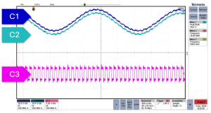
Figure 1: Scope Trace
A plain scope probe can narrate a grand story. At 500 kHz, it is not unusual to observe differential signals severely distorted due to external coupling. The transceiver receives data swathed in extraneous noise, and communication becomes unstable.
The 1983 EIA-485 standard provided for such situations by specifying a large common mode voltage range of -7 V to +12 V. Theoretically, this would be safe for signals. Practically, long cable lengths, wire resistance, and common mode external interference can move common mode levels far beyond that range.
Sources of Common Mode Swings:
A number of real-world conditions can inject interference currents into RS-485 networks:
- Motors and High-Voltage Power Supplies

Figure 2: Common Mode Swing Sources – Motors and High Voltage Power Supplies
Motors used in industry and switching power supplies produce powerful electromagnetic fields. These fields tend to couple readily into surrounding cabling, inducing unwanted RF interference on the data lines.
- Power and Data Bundled Together

Figure 3: Common Mode Swing Sources – Cables with Power and Data Bundled Together
Running AC power cables alongside RS-485 data cables within the same cable causes capacitive coupling, which injects currents directly into the communication network.
- Ground Potential Differences Between Buildings

Figure 4: Common Mode Swing Sources – Ground Potential Differences Between Buildings

Figure 5: Ground Voltage Differences Explained
When networking across buildings, ground potential differences can create large voltage shifts. Leakage currents from safety grounds or neutral wiring often raise the common mode voltage, pushing it outside the RS-485 tolerance.
Why Extended Common Mode Range Transceivers Help
Rather than depend solely on costly shielded cables, a better solution is to implement RS-485 transceivers that have wider common mode ranges. These chips are designed to maintain reliable data transfer even when external noise forces voltages well outside the legacy standard.
Examples include:
MAX33070E – MAX33074E: Half-duplex, 3.3 V to 5 V products with ±40 V common mode tolerance
LTC2862A and LTC2863: Half- or full-duplex products with improved noise immunity
Through the implementation of these resilient solutions, engineers are able to safeguard networks against downtime, minimize field failures, and lengthen the lifespan of industrial systems.
Conclusion:
Installing and operating RS-485 networks under regulated settings is nearly impossible. Motors, power supplies, bundled cables-if anything-shift voltages around in ways that disrupt communication.
With that said, the way to go will be to design with extended common mode range transceivers that offer a safety margin against any such disruptive swings and thus ensuring communication stays steady and reliable even in the harshest industrial weather.
(This article has been adapted and modified from content on Analog Devices.)
The post Handling Signal Swings: Wide Common Mode Range in Action appeared first on ELE Times.
Сторінки

