
EDN Network

Mic balances low power use with high audio quality

The IM69D129F low-power MEMS microphone, part of Infineon’s XENSIV lineup, helps extend battery life in portable devices. In high-performance mode, it consumes only 450 µA at 3.072 MHz, dropping to just 170 µA at 768 kHz in low-power mode.

Designed for space-constrained designs, the IM69D129F provides reliable audio performance with a 69-dB(A) SNR in a compact 3.50×2.65×0.98-mm package. Infineon’s sealed dual-membrane (SDM) technology adds IP57-rated protection again water and dust, making the microphone well-suited for active noise cancellation (ANC) headphones and earbuds, voice-enabled devices, laptops, tablets, conference systems, and cameras.
The IM69D129F microphone integrates a low-noise preamplifier and a sigma-delta ADC, delivering digital pulse density modulation (PDM) output for seamless use in modern audio systems. Its 11-Hz flat frequency response and ±1-dB sensitivity tolerance enable accurate audio capture across multi-microphone arrays.
The IM69D129F is available to order, with customer samples offered on request.
The post Mic balances low power use with high audio quality appeared first on EDN.
Tiny resonators unlock ultra-compact devices

SiTime’s Titan series of MEMS resonators occupy 4× to 12 × less PCB area than the smallest legacy quartz crystal alternatives. Their 0.46×0.46-mm chip-scale package enables miniaturization in small battery-powered devices such as wearable/implantable medical devices, smart watches, fitness rings, smart home sensors, and industrial IoT trackers.

Built on the company’s sixth-generation FujiMEMS technology, the Titan platform delivers improved performance and reliability compared to quartz resonators. Key benefits include:
- Small footprint: 0505 CSP saves up to 7× PCB area versus 1210 quartz and 4× versus 1008 quartz.
- Low power: Reduces oscillator circuit consumption by up to 50%.
- Fast startup: Starts up to 3× quicker with 3× lower startup energy.
- Improved aging stability: Up to 5× better, specified for 5 years at maximum temperature.
- Tight temperature stability: Maintains performance from –40°C to +125°C.
- Enhanced mechanical resilience: Withstands up to 50× more shock and vibration.
The Titan family of resonators comprises five devices, ranging from 32 MHz to 76.8 MHz. Production samples of the 32‑MHz SiT11100 are available now. Engineering samples of the remaining devices—38.4‑MHz SiT11102, 40‑MHz SiT11104, 48‑MHz SiT11103, and 76.8‑MHz SiT11101—will be available starting December 15, 2025.
The post Tiny resonators unlock ultra-compact devices appeared first on EDN.
Bluetooth LE 5.4 module adds edge programmability

A pre-certified module with edge intelligence, the Digi XBee 3 BLU provides secure Bluetooth LE 5.4 connectivity for industrial IoT. Embedded MicroPython programmability with access to on-module I/O enables the implementation of custom logic, sensor data processing, and decision-making at the edge.

Based on Silicon Labs’ EFR32MG transceiver, the XBee 3 BLU interoperates with Bluetooth LE 5.4 devices that support 1M (1-Mbit/s) and 2M (2-Mbits/s) PHY modes. It provides +8-dBm transmit power, -97-dBm receiver sensitivity, and beaconing capabilities for proximity detection and asset tracking. The module operates across a temperature range of -40°C to +85°C.
The XBee 3 BLU is offered in two standard XBee form factors—through-hole and micro—and comes pre-certified to speed regulatory approvals worldwide. Built-in Digi TrustFence delivers secure boot, protected JTAG, and hardware-accelerated encryption. The module also supports the Secure Remote Password (SRP) protocol for zero-knowledge authentication and 256-bit AES encryption.
The XBee 3 BLU module and development kits are now available through Digi’s authorized distributors.
The post Bluetooth LE 5.4 module adds edge programmability appeared first on EDN.
Low-power 32-bit MCUs enable touch HMIs

Entry-level MCUs in the Renesas RA0L1 group combine low current consumption with capacitive touch sensing for responsive HMIs. A 32-bit Arm Cortex-M23 core running at 32 MHz makes them well-suited for consumer electronics, appliances, industrial control, and building automation.

The devices draw 2.9 mA in active mode and 0.92 mA in sleep mode. Fast wakeup lets them remain in software standby longer, where power drops to just 0.25 µA—reducing current consumption by up to 90% compared with other MCUs, according to Renesas.
The RA0L1 devices target cost-sensitive applications with up to 64 KB of code flash, 16 KB of SRAM, and a 1.6-V to 5.5-V operating range that removes the need for level shifters in 5-V systems. A high-speed on-chip oscillator with ±1.0% precision ensures baud rate accuracy without a standalone oscillator, maintaining stability from -40°C to +125°C. Integrated communications, analog, safety, and security functions help cut BOM cost.
RA0L1 MCUs are available now in a variety of packages, including a compact 4×4-mm, 24-pin QFN.
The post Low-power 32-bit MCUs enable touch HMIs appeared first on EDN.
Pressure washer recall and aluminum electrolytic capacitors
I recently came across a disturbing piece of news about a recall of Ryobi pressurized washers on FOX Business (Figure 1). I got some pictures from there and elsewhere, which, with a little rearrangement and supplementation, point out a very real danger.
 Figure 1 Screenshot of the news article on the pressure washer recall. Source: Fox Business
The so-called overheating capacitors can apparently be identified as shown in Figure 2.

Figure 2 The overheating motor starting capacitor under question. Source: Amazon.com
This component provides 300 µF, which is a magnitude of capacitance that can only be obtained in aluminum electrolytic capacitors. Such capacitors cannot be allowed to experience reverse voltage, though, so to achieve the 250 VAC capability, a pair of capacitors must be used in series as shown in Figure 3.

Figure 3 Capture of a schematic that combines two aluminum-electrolytic capacitors.
Each capacitor is paired with a diode that limits the reverse polarity that can appear across each capacitor to one forward diode voltage drop, call that 0.7 V. Supposedly, that voltage limit is still safe as reverse voltage across an aluminum electrolytic capacitor.
However!!!! If one diode fails as an open circuit, the reverse voltage that can be imposed on its associated capacitor can rise way above the diode limit, and that capacitor can fail.

Figure 4 A SPICE example of reverse voltage when one diode fails as an open circuit. Source: John Dunn
Such a failure can lead to a capacitor explosion.
When I was in college, I had a lab partner with whom I would perform each class experiment. One experiment involved a 22-µF 16-V electrolytic capacitor. It was a tiny little thing.
Unfortunately, my partner (It was NOT me!) put that capacitor in the circuit board backwards, and it was driven into reverse bias. It sat there for a while as the two of us were discussing the circuit under test when suddenly that capacitor exploded!!
That explosion was LOUD!! Everybody within fifty feet was looking in our direction. The aluminum shell of the capacitor had been torn open like a Tootsie Roll wrapper.
I suspect that the Ryobi capacitor issue was not from “overheating” as Figure 5 suggests, but that one of the diodes within the CD60 capacitor failed as an open circuit, which allowed excessive reverse bias to appear across its associated capacitor. (If a diode had failed as a short circuit, I doubt if the motor would start.)

Figure 5 An unwise reassurance that the capacitor may not blow when installed backwards. Source: LeftyMaker, YouTube
One would think that the CD60 capacitor would have a pressure release plug that would vent if internal pressure got too high. If there is such a mechanism, it seems that sometimes it is not working properly. The sheer physical size of the CD60 capacitor in the Ryobi product versus that little itty-bitty capacitor in my lab class makes me think of the CD60 capacitor as a potential hand grenade.
John Dunn is an electronics consultant and a graduate of The Polytechnic Institute of Brooklyn (BSEE) and of New York University (MSEE).
Related Content
- Would better electrolytic capacitors reduce e-waste?
- Capacitors–the old decoupling standbys
- Ensure long lifetimes from electrolytic capacitors: A case study in LED light bulbs
- Determining end-of-life, ESR, and lifetime calculations for electrolytic capacitors at higher temperatures
- Power Tips #50: Avoid these common aluminum electrolytic capacitor pitfalls
The post Pressure washer recall and aluminum electrolytic capacitors appeared first on EDN.
High-speed digitizer boasts open FPGA architecture

High-speed data acquisition is made simple with a 12-bit digitizer that offers up to 10 GSPS sampling rate and 2 Gbyte/s sustained data transfer to a host PC. Teledyne’s ADQ3-series digitizer provides high-performance data acquisition in a compact, standalone USB 3.2 form factor.
Digitizers—crucial in analytical and sensing systems such as automated test equipment (ATE), distributed fiber optic sensing platforms, LiDARs, mass spectrometers, and swept-source optical coherence tomography—are undergoing a transformation amid growing demand for faster data acquisition. It inevitably calls for higher resolution, faster imaging speeds, and more granular real-time analysis.
That’s because new use cases in sensing systems generate gigabytes of data per second, demanding efficient real-time processing and high-speed data transfer. Then there is the issue of preserving signal integrity in compact and noise-sensitive environments, which mandates compact form factors that can be placed close to the detector within the system enclosure.
ADQ3-USB, housed in a robust, fanless enclosure, allows engineers to place the digitizer close to the detector. This also minimizes cable length and reduces signal reflections, a crucial factor for optimizing analog performance in high-speed applications.

ADQ3-USB is compatible with a wide range of digitizer models within the ADQ3 series, including ADQ30, ADQ32, ADQ33, and ADQ35. Source: Teledyne SP Devices
ADQ3-USB features onboard FPGA capabilities for real-time signal processing. That enables it to support continuous data streaming at up to 2 Gbyte/s via USB 3.2. Moreover, even large volumes of raw data up to 20 Gbyte/s can be efficiently reduced and transferred without bottlenecks.
Next, it eliminates the need for PCIe slots, leading to fast and simple integration with mini-PCs and laptops. This also makes it suitable for mobile setups, embedded systems, and OEM applications.
ADQ3-USB’s open FPGA architecture also allows design engineers to implement application-specific algorithms directly on the 1/2 digitizer. That, in turn, reduces the need for post-processing and enables real-time decision-making.
Finally, this digitizer supports multiple firmware packages tailored to specific application needs. That includes FWDAQ for standard data acquisition, FWATD for waveform averaging, FWPD for pulse detection, and DEVDAQ for custom FPGA development.
Related Content
- Analysis of large data acquisitions
- Data acquisition systems and SoCs—A guide
- Trending into data-acquisition: a mini-study in contrasts
- Data Acquisition and Instrumentation: The DAS and Sensors
- Data Acquisition and Instrumentation: Data Processing and Calibration
The post High-speed digitizer boasts open FPGA architecture appeared first on EDN.
Capacitor matchmaker

Precision-matched capacitor pairs are commercially available items, but only in a limited range of values, working voltage, and dielectrics.
Plus, sometimes an extra critical application with extra tight tolerances (or an extra tight budget) can dictate a little (or a lot) DIY. For example, see “Inherently DC accurate 16-bit PWM TBH DAC.”
Wow the engineering world with your unique design: Design Ideas Submission Guide
Figure 1’s matchmaker circuit can help make the otherwise odious chore of searching through a batch of parts for accurately matching pairs quicker and a bit less taxing. Best of all, it does precision matchmaking (potentially to the ppm level) with no need for pricey precision reference components.
Here’s how it works.

Figure 1 Flip-flop U2b generates complementary excitation of the A and B capacitors under test.
Complementary (equal but opposite) excitation of the A and B capacitors under test implies that if Ca = Cb, then the charges passed will exactly cancel out, yielding a null at OUTPUT. If they differ, however, then an integrated output signal of 50 mV per % of mismatch will result if C3, C5, C4, and Cab (capacitors randomly selected from the trial batch) are equal in value, e.g., 0.68 µF. This signal is synchronously rectified by U1b, then integrated and buffered by the U1c and A1 feedback loop.
If Ca > Cb, the “A > B” output polarity will be positive relative to “B > A”. The reverse is also true: If Cb > Ca, the “A > B” output polarity will be negative relative to “B > A”.
Resolution of the match measurement will depend on the voltage resolution of the digital voltmeter (DVM). If that’s 1 mV, then matching to ±1/50th of 1%, or ±0.02%, will be possible. If it’s 100 µV (typical of a standard 3¾ digit multimeter with a 300 mV scale), then matching to ±0.002%, i.e., ±20ppm, is doable. And so on…
Measurement gain is inversely proportional to C4. So, if you need more resolution, simply decrease C4 to gain gain.

Figure 2 The U1aU2a multivibrator waveforms; the green waveform is the R3R4 junction, and the red waveform is U2 pin 6. The frequency is 0.1mHz/C3.
Note that the U1aU2a clock’s frequency precision and stability is somewhat dubious (even if we’re charitable). Happily, the accuracy of the ultimate Ca/Cb match doesn’t depend on a stable clock. Neither does match accuracy depend on the output impedances of D2b’s complementary outputs, not even on their symmetry!
Both insensitivities derive from the fact that it’s the transferred charge that forms the basis of matchmaking precision, and therefore neither current nor voltage matters very much.
However, due to the temperature sensitivity of some dielectrics, it’s probably a good idea to handle tested devices with thermally insulating gloves. This will save time and frustration waiting for them to equilibrate, not to mention possible outright erroneous results. Those are also known to cause frustration!
My thanks go to frequent contributor Christopher Paul for suggesting the utility of capacitor precision matching, and as always, to DI editor Aalyia Shaukat for this marvelously productive DI EE ecosystem we inhabit.
Stephen Woodward’s relationship with EDN’s DI column goes back quite a long way. Over 100 submissions have been accepted since his first contribution back in 1974.
Related Content
The post Capacitor matchmaker appeared first on EDN.
Class D: Audio amplifier ascendancy

Last month, an interesting Class AB audio amplifier was in the spotlight, a monoblock-configured pair of which I’m actually listening to (Widespread Panic’s Light Fuse Get Away, to be precise) as I type these follow-on words:

This time, it’s Class D’s turn in the spotlight. Here’s a summary link to EDN’s voluminous coverage of the technology over the past few decades, and a Wikipedia’s summary:
A class-D amplifier, or switching amplifier, is an electronic amplifier in which the amplifying devices (transistors, usually MOSFETs) operate as electronic switches, and not as linear gain devices as in other amplifiers. They operate by rapidly switching back and forth between the supply rails, using pulse-width modulation, pulse-density modulation, or related techniques to produce a pulse train output. A simple low-pass filter may be used to attenuate their high-frequency content to provide analog output current and voltage. Little energy is dissipated in the amplifying transistors because they are always either fully on or fully off, so efficiency can exceed 90%.
Tripath, which branded the technology as “Class T”, was the first mainstream-volume supplier of Class D technology. My first exposure to Class D stretches back nearly 30 years, to 2007 when I first met with (and auditioned prototype gear from) D2Audio and its always entertaining (meant as a compliment), not to mention well-informed, Chief Technology Officer Skip Taylor at CES. I subsequently sic’d Skip on my then-colleague, EDN then-Analog Editor Joshua Israelsohn, who had a number of enjoyable mind-melding (maybe also melting?) meetings with Skip and his colleagues. Intersil bought D2Audio a year later, preceded by Texas Instruments’ 2000 acquisition of Burr-Brown and followed by Infineon’s 2018 purchase Merus Audio and Analog Devices’ 2021 Maxim buy (all as trend examples, not intended to be a comprehensive list)…and Class D technology was off to the races.
Class D vs Class ABHere’s another take on Class D versus the Class AB (and A, for that matter) precursors, from Paul McGowan, the co-founder and CEO of high-end audio equipment supplier PS Audio, whose “Ask Paul” ongoing video series is both entertaining and educational, therefore highly recommended:
That this video comes from Paul (and PS Audio, located just “up the road” from me in Boulder, CO, for that matter) is highly revealing, I think. Audiophiles, the nexus of PS Audio’s customer base, are generally speaking both change-adverse and perversely picky when it comes to perceived quality. That they, who D2Audio was specifically targeting with its demos way back in 2007, were among the first to adopt Class D amplifier technology tells me a few things:
- With all due respect to Schiit co-founder Jason Stoddard, his diatribe about Class D’s tendency to “hiss like a demon cat, drilling slowly into your synapses and draining your soul” is dated and overstated, IMHO at least. As I noted last month, “he might have been right about Class D a few years ago, especially in the near-field configurations he’s specifically advocating for Rekkr, but no longer.”
- More generally, the technology has for a while now been good enough for audiophiles, so I’d wager it’s also good enough for the masses.
- And why was it appealing to audiophiles? Cost for them is a secondary-at-most concern, right? Well, their listening rooms tend to contain massive speakers, requiring formidable amounts of power to drive them. And, as Wikipedia notes, “The major advantage of a class-D amplifier is that it can be much more efficient than a linear amplifier, dissipating less power as heat in the active devices…also, given that large heat sinks are not required, class-D amplifiers are much lighter weight than class-A, -B, or -AB amplifiers.”
Lighter…and much smaller, too. In the spirit of “a picture paints a thousand words,” here are some examples. First off, here again is the Class AB-based Rekkr (Internet Archive cache link), which is sound-spec’d as follows:
- Stereo, 8 Ohms: 2W RMS per channel
- Stereo, 4 Ohms: 3W RMS per channel
- Mono, 8 Ohms: 4W RMS
with the following form factor-related specs:
- Size: 5” x 3.5” x 1.25”
- Weight: 1 lbs


Next up is its Gjallarhorn “big brother”, also Class AB-based, also mentioned (but not shown) in last month’s piece, and sound-spec’d as follows:
- Stereo, 8 Ohms: 10W RMS per channel
- Stereo, 4 Ohms: 15W RMS per channel
- Mono, 8 ohms: 30W RMS
with the following form factor-related specs:
- Size: 9” x 6” x 2.5”
- Weight: 8 lbs


Here’s a visual comparison of their respective form factors:


Foreground, then background, focus:


Ditto:


Keen-eyed readers may have already noticed that the comparison’s not entirely fair, since the Gjallarhorn integrates the AC/DC conversion circuitry that’s alternatively placed (at least partly) in the Rekkr’s external AC/AC “wall wart”. But as you can see, the Rekkr PSU is pretty tiny, so…:


Now for the Class D competitors (and, I’d generally argue, successors). Earlier this year, ahead of the looming tariffs, I acquired three different “Chi-Fi” manufacturer/model combinations…not counting the Class D circuitry inside the powered speakers I already owned…or my latest network audio streamer…or my latest sound bar (from Yamaha, replacing the Hisense unit I complained about in May)…all of which you’ll hear more about in other blog posts to come…
The first was a monoblock-only unit, the Fosi Audio V3 Mono:


Its (again, mono in this case) output specs, along with those of the other two devices I’ll be showcasing today, vary depending on the capabilities of the power supply connected to it:
- Rated Power Output : 48V/5A–240W@4Ω ; 32V/5A –100W@4Ω
And here are its form factor details:
- 6 x 4.2 x 1.6 inches (142mm x 105mm x 35mm)
- 06 pounds (0.48)
The second is Douk Audio’s A5, a dual-channel (stereo) Class D amp:

 Again, its output specs are power supply voltage-and-current, as well as speaker impedance, dependent. Douk Audio provides more granular detail on its website than Fosi Audio does even in the V3 Mono user manual, unfortunately. But the general trend is similar in practice, given that they’re both based on Texas Instruments’ TPA3255 chipset:
|
Power Supply |
Speaker Impedance |
Rated Output Power |
|
32V/5A |
4Ω |
78W+78W |
|
32V/5A |
6Ω |
71W+71W |
|
32V/5A |
8Ω |
65W+65W |
|
36V/6A |
4Ω |
107W+107W |
|
36V/6A |
6Ω |
100W+100W |
|
36V/6A |
8Ω |
94W+94W |
|
48V/5A |
4Ω |
120W+120W |
|
48V/5A |
6Ω |
110W+110W |
|
48V/5A |
8Ω |
102W+102W |
|
48V/10A |
4Ω |
250W+250W |
|
48V/10A |
6Ω |
210W+210W |
|
48V/10A |
8Ω |
185W+185W |
And its form factor details? Here you go:
- Dimensions (W*D*H): 95*92*50 mm/3.74*3.62*1.97 in
- Net weight: 506 g/1.12 lb
Last, but definitely not least, is a more recent Douk Audio device upgrade, the A5 Pro, adding both a Bluetooth receiver and a separate headphone output amplifier:


Same TI TPA3255-based audio power amplifier subsystem as with the base A5, so same output specs as shown earlier. The form factor is tweaked a bit (but only a bit, and likely mostly-to-completely to just make room for more knobs-and-such on the front panel), however:
- Dimensions (W*D*H): 130*112*33 mm/5.12*4.41*1.30 in
- Net weight: 525 g/1.16 lb
That’s the last of the stock shots, at least for a while; now for some more “real life” ones. First off, here’s how the Schiit Rekkr stacks up (literally) against the Fosi Audio V3 Mono, which is capable of up to (speaker impedance- and power supply-dependent) more than 50x the mono output power at comparable distortion:


How about the Schiit Gjallarhorn versus the Fosi Audio V3 Mono? Glad you asked. Again, as a reminder, the latter has ~8X the mono output power in this case, with its beefiest power supply option and when driving the same impedance and at similar (inaudible) distortion levels. Not to mention being half the price (or even less, depending on where it’s sourced and how it’s kitted):


Again, a two-photo foreground-then-background focus shift:


Once again, the detail-oriented among you will point out that the Gjallarhorn chassis also encompasses AC/DC conversion circuitry, external to (and not shown in) the Fosi Audio case. You’re right, although there was a method to my madness. I didn’t want to show three sets of vs-V3 Mono photos, one set with each of the three PSUs I have in my possession: 32V/5A, 48V/5A and 48V/10A. Instead, here are the standalone undersides of the power supplies, capable of being used with any of the three Class D amplifiers I’m covering today. 32V/5A first:


Now 48V/5A:


And finally, the “Big Kahuna” 48V/10A version:


And here they are stacked on top of each other, with the 32V/5A one on top and (obviously) the 48V/10A one on the bottom:


Independent reviews suggest that the incremental power output of the Fosi Audio V3 Mono tails off beyond the 48V/5A point…the Douk Audio units’ additive output performance increases more linearly at 48V/10A, but that’s to be expected as there are two audio power amplifiers—one for each channel—inside. But there’s another reason to run the Fosi Audio V3 Mono—two of them, actually—with a 48V/10A source. In such a configuration, the company also sells what it calls a “DC Power Filter”, which (in conjunction with an appropriate cable option) splits the 10A input current evenly among both of its outputs, enabling a single PSU to concurrently fuel two amplifiers:


I own two DC Power Filters. One came bundled with a two-amplifier set I bought off eBay. The other was a standalone purchase from Fosi’s online store, used with two other V3 Mono amps I got individually (for reasons I’ll explain further in a teardown to come!):


What about those two Douk Audio units? Here’s the A5, alongside the 48V/5A power supply it came bundled with, on top of the Schiit Gjallarhorn:


Now for its A5 Pro “big brother”:


Because I couldn’t resist, the following shots prove that (after dispensing with the PSUs), I could fit both Douk Audio devices on top of a Gjallarhorn:


And in closing, here are all three of today’s Class D devices stacked on top of each other, showcasing their form factor similarities:


Wrapping up, there are a couple of other points I wanted to note. First off, all three of the Class D amps support (believe it or not) user-accessible op-amp swapping:


analogous to the “tube rolling” of times past (and present, for some folks, and potentially others, too…there is, after all, a Vali 2++ now sitting at the top of the Schiit stack on my desk):

Finally, what’s with the “PFFB” promotion prominent on both manufacturers’ websites?


It stands for Post-Filter Feedback, and understanding what it is and does first requires a step (or few) back. Although, as the Wikipedia Class D definition I shared at the beginning of this piece noted, “A simple low-pass filter may be used to attenuate their high-frequency content to provide analog output current and voltage,” in practice the output filtering circuitry tends to be notably more complex than this; to render inaudible the otherwise distorting aforementioned “hiss like a demon cat”, for example, to suppress phase shift artifacts, etc. To reiterate on this circuit’s robustness importance, I’ll turn you over to Paul McGowan again for more on the topic:
PFFB, implemented in TI’s TPA3255 (and others), is the latest evolution in this output filtering scheme. Quoting from Google’s AI Overview summary of the search topic:
PFFB, or Post-Filter Feedback, is a secondary feedback loop in Class-D amplifiers that takes a portion of the signal after the LC output filter and feeds it back to the input to improve audio quality. This technique reduces distortion and improves the linearity of the power stage and output filter components, particularly the inductor, which is a primary source of distortion. PFFB also increases load independence, meaning the amplifier’s performance is less affected by the specific loudspeaker connected.
Here’s a visible example of PFFB’s benefits. First off, an output level-vs-frequency plot from Audio Science Review’s evaluation of the Fosi Audio V3 Mono:

Requoting highly recommended content expert (and long-time personal collaborator) Amir Majidimehr, “There is essentially no impact up to 20 kHz between the 4 and 8 ohm, indicating very low output impedance, albeit with a bit of peaking. Compare that to non-PFFB amps such as Fosi Audio V3 stereo amp:”

The TL;DR (at the end of another long writeup…sorry!) summary of Amir’s findings (and PFFB’s benefits): it suppresses an amplifier’s perceived loudness from otherwise varying with output frequency, not that this arguably was perceptible much if at all previously, candidly (specifically because the variability tended to occur at high frequencies, hard for all but the “golden ears” among us to discern, anyway). But since it now “comes along for the ride” with modern Class D amplifier designs anyway, at little if any incremental cost and with no sonic downside…
With that, encroaching on the 2,300-word threshold, I’m going to sign off for today. More on this topic, including the earlier-promised Class D amplifier teardown, to come soon. Until then, “sound off” with your thoughts in the comments!
—Brian Dipert is the Editor-in-Chief of the Edge AI and Vision Alliance, and a Senior Analyst at BDTI and Editor-in-Chief of InsideDSP, the company’s online newsletter.
Related Content
- Audio amplifiers: How much power (and at what tradeoffs) is really required?
- EDN Class D amplifier coverage
- Class D audio power amplifiers: Adding punch to your sound design
- The truth about Class D amplifiers
The post Class D: Audio amplifier ascendancy appeared first on EDN.
Tektronix releases its new high-performance 7 Series oscilloscope

Today, Tektronix, i.e., Tek, releases its high-performance oscilloscope: The 7 Series digital phosphor oscilloscope (DPO) (Figure 1). This scope is a replacement of its discontinued (but still sought-after) 70000 series, using the same probe set.
 Figure 1 7 Series DPO is a replacement to the legacy 7000 series with the same probe performance, but much lower SNR, ENOB, throughput, and user-friendly touchscreen interface. Source: Tektronix
In a conversation with Tektronix’s Tim Bieber, Principal Product Planner, described the motivation for the new series, “Every 10 to 15 years, we have to replatform instruments because parts get old and the technology moves forward.” This scope is a direct response to the demand after conjoint analysis, or market research that Tek has done over the years with their established customer base.
A user-friendly, high-performance Tek scopeThe 7 series DPO oscilloscope is the high-performance version of the 2 through 6 series of MSOs, where each series is optimized for different performance capabilities and price points (Figure 2). The unifying factor across this entire portfolio is the user interface (UI) and TekScope PC analysis software developed over a decade ago that allows for remote access to the benchtop instrument as well as offline analysis.

Figure 2 The 2 through 7 Series of Tektronix scopes, all using the same UI and analysis software. Source: Tektronix
“There are customers that want the raw data and don’t do anything with it, but there are other customers that need fairly complex measurements,” said Bieber when highlighting the importance of the analysis software piece of the modern oscilloscope puzzle, “For example, PCIe’s latest generation electrical spec is about 1000 pages long and there’s a couple chapters that go through all the measurements. Very few customers will want to go and develop all these measurements, so they look to the scope vendor to develop that, and we’ve had a package that we’ve had for 20 years.”
SpecificationsTable 1 offers a comparison of the new 7 Series DPO and the older DPO70000 oscilloscopes. The 7 Series DPO is a replacement for the DPO70000 series with all “TekConnect” channels that offer a comparable analog bandwidth from DC to 33 GHz. The TekConnect adapters (TCA) provide less signal distortion than other traditional adapters, such as BNC-to-N or N-to-SMA adapters.
Tek also offers an Asynchronous Time Interleaving (ATI) architecture in the DPO70000 series, which provides a considerably larger bandwidth via 1.85 mm connectors. Bieber clarified why ATI was not included in the 7 Series DPO, stating that for the current models, which range from DC to 25 GHz, only TekConnect channels are necessary. He added that future 7 Series models with higher bandwidths will incorporate higher bandwidth connectors, such as 1.85 mm connectors.
|
7 Series DPO |
DPO70000 |
||
|
Channel type |
TekConnect channels |
TekConnect channels |
ATI channels |
|
Number of channels |
4 analog |
2 to 8 analog |
1 to 2 analog |
|
ADC |
10-bit |
8-bit |
8-bit |
|
ENOB (500 mV full scale, signal 90% of full scale) |
7.5 bits at 8 GHz to 6.5 bits at 25 GHz |
5.1 bits at 8 MHz and 4.8 bits at 25 GHz (for 33 GHz, 100 GS/s) |
4.9 bits at ~8 GHz and 4.6 bits at ~25 GHz (for 70 GHz, 200 GS/s ATI channel) |
|
Analog bandwidth |
8 GHz to 25 GHz (customer upgradeable) |
13 to 33 GHz |
50 to 70 GHz |
|
Sample rate per channel |
125 GS/s on all 4 channels |
100 GS/s |
200 GS/s |
|
Record length |
500 Mpoints (up to 2 Gpoints option) |
62.5 Mpoints (up to 1 Gpoints option) |
62.5 Mpoints (up to 1 Gpoints option) |
|
Random noise |
0.10% of full scale to 0.23% of full scale, 500 mV full scale |
0.69% to 0.83% of full scale, 300 mV full scale |
0.43% to 0.71% of full scale, 500 mV full scale |
|
Intrinsic jitter |
60 fs (1 µs time duration) and 70 fs (1 ms time duration) |
100 fs (10 µs time duration) |
65 fs (10 µs time duration) |
|
Probe compatibility |
P7700 and P7600 Series TriMode |
P7500, 7600, and P7700 Series TriMode |
|
|
Connectivity |
LAN (10G Ethernet on SFP+ and 1000 Base-T on RJ45), USB 3.0 (7 total), DisplayPort, HDMI |
PCIe, USB, Thunderbolt, HDMI, DisplayPort, and more |
|
|
Screen size |
15.6-inch HD touchscreen |
Not specified, but much smaller |
|
 probe
probe Table 1: A comparison of the newly released 7 series DPO and the older 70000 series.
The 7 Series DPO offers significant performance upgrades over the 70000 series. These enhancements are primarily due to three key improvements in its TekConnect channels:
- Lower learning curve with the TekScope user interface (UI) that would be familiar to Tek customers
- A fast throughput with a 10 Gb Ethernet LAN SFP+ port (on the back of the oscilloscope)
- A clean signal path due to the iterative advancements, yielding two new ASICs, the Tek079 and Tek085, both designed and built in-house
The 10 Gb Ethernet LAN SFP+ port (Figure 3) is ideal for short data runs with a swift offload from the scope for parallel analysis and off-scope processing. Additionally, the faster CPU and on-board GPU will accelerate data processing directly on the scope.

Figure 3 An image of the back of the 7 Series showing the 10 Gb Ethernet LAN SFP+ port, which can accept either a regular RJ45, fiber optic, or direct-attach connection. Source: Tektronix
The new ASICsAt the core of the oscilloscope are the upgrades to the custom preamplifier and ADC, as shown on the acquisition board in Figure 4. Each of these boards has two channels; the signal enters through the inputs to the preamp and ADC, and out to a large FPGA used for triggering and data storage.

Figure 4 The 7 Series DPO acquisition board showing Tek085 preamplifiers connected directly to the Tek079 ADC (black chips shown on the left-hand side). Source: Tektronix
“This chip (Tek85) has half the noise of the previous preamp called Tek61, which is in our 6 Series product,” said Bieber. The Tek85 chip is fabricated using GlobalFoundries’ 9HP SiGe process. It uses “Quiet Channel” noise reduction technology, which essentially performs the continuous time linear equalization (CTLE) function in hardware instead of software to push channel noise down without increasing the noise floor (a consequence of implementing equalization techniques in software). This, along with the 10-bit ADC, allows the oscilloscope to have a low vertical (random) noise with a high effective number of bits (ENOB).
The addition of the 7 Series offers a clear upgrade to the older 70000 variant while also benefiting from the enhanced UI/UX of the established 2 through 6 Series Tek scopes.
Aalyia Shaukat, associate editor at EDN, holds a Bachelor’s degree in electrical engineering and has worked in the design publishing industry for nearly ten years.
Related Content
- Oscilloscope articles by Art Pini
- Tektronix MDO4000 oscilloscopes go multifunction
- A new cost-optimized high-performance oscilloscope
- Building a low-cost, precision digital oscilloscope—Part 1
The post Tektronix releases its new high-performance 7 Series oscilloscope appeared first on EDN.
Putting 3D IC to work for you

3D IC chiplet-based heterogeneous package integration represents the next major evolution in semiconductor design. It allows us to continue scaling system performance despite the physical limitationA sneak peak at 3D IC design toolkits and workflowss of traditional monolithic chip manufacturing. By breaking functional systems into sub-functional chiplets and using advanced packaging integration technologies, we can create more complex, more powerful systems than ever before.
The challenge—and opportunity—for the industry is to lower the barriers to adoption of 3D IC design so that its benefits can become available industry-wide and not just the bleeding edge markets. Thus, the Chiplet Design Exchange (CDX) was formed within the Open Compute Project with the mission of developing easy-to-use, machine-readable design kits (3DKs).
With participation from EDA vendors, foundries, OSATs, and materials providers, the goal was to define standards and workflows for 3D IC design. In other words, a neutral, open foundation that enables efficient chiplet integration and reuse, accelerates innovation, and guarantees manufacturability across organizational boundaries.
3D IC design toolkits and workflows
Silicon IC design is supported by a mature ecosystem of IP libraries and standardized process design kits, but advanced packaging has historically lacked a similar infrastructure. 3D IC design requires new, specialized design kits tailored for chiplet-based workflows and advanced package integration complexity.
The CDX group, together with industry partners, defined four primary 3DK categories, each supporting a discrete aspect of 3D IC design, integration, and verification:
- Chiplet design kits (CDKs) provide standardized, reusable chiplet models with the necessary information for seamless system integration.
- Package assembly design kits (PADKs) define essential package rules such as I/O/TSV pitch, substrate and interposer spacing, and component placement guidelines to facilitate manufacturability.
- Material design kits (MDKs) contain composite material properties needed for accurate electrical and reliability simulations.
- Package test design kits (PTDKs) specify test I/O, pin dimensions, and functions, supporting robust automated testing at both the chiplet and system-in-package level.

Figure 1 A chiplet design kit (CDK) is shown as per the JEDEC JEP30 part model. Source: Siemens EDA
Standardizing these kits in machine-readable, EDA-neutral formats closes persistent gaps between silicon, packaging, and test communities. Every stakeholder—whether chiplet vendor, package architect, or manufacturing partner—can contribute, access, and leverage accurate models for design, verification, and production handoff to manufacturing.
The wider availability of 3DKs is driving the emergence of new, fluid 3D IC workflows. Chiplet suppliers can now publish detailed, standards-compliant digital models, creating a catalog of validated IP. Designers can search, evaluate, and select chiplets based on electrical, physical, and performance characteristics—similar to how SoC developers choose IP blocks for traditional integration. This enhances discoverability, accelerates design cycles, and fosters a new business model for silicon IP reuse.
Crucial to this flow is automation in model authoring. Manually crafting CDX-compliant 3DKs at scale is not practical, so the industry is investing in open-source, EDA-neutral authoring tools. Siemens EDA Innovator3D IC exemplifies this trend, providing a unified environment where teams can design, verify, and plan manufacturing in one cockpit. These platforms enable rapid iteration, simulation, and validation of heterogeneous integration, helping organizations reduce costly design spins and reach the market faster.

Figure 2 The Innovator3D IC Integrator facilitates a heterogeneous integration cockpit. Source: Siemens EDA
The AI and 3D IC alliance
Artificial intelligence (AI) and high-performance computing (HPC) are both driving, and benefiting from, progress in 3D IC technology. As scaling of traditional process nodes approaches its physical limits, chiplet integration and advanced packaging become the primary pathways to higher performance and capacity. By stacking high-bandwidth memory near logic, designers achieve higher data transfer rates with reduced latency and power—vital for AI, hyperscalers, and data-intensive applications.
The industry is also crossing new thresholds: single-die reticle limits are being surpassed, and panel-scale organic and glass interposers now support the assembly of thousands of chiplets—resulting in systems with trillions of transistors on a single substrate. The complexity of designing, laying out, and verifying these massive architectures is well beyond the reach of traditional manual processes, especially as electrical, power, thermal, and mechanical dependencies multiply.
AI is therefore becoming an indispensable partner, not just another tool. Machine learning accelerates fundamental EDA tasks, such as SPICE simulation, by orders of magnitude and powers multi-dimensional optimization engines that explore a vast design space automatically. Recent advances allow even legacy tools to achieve significant productivity gains by learning from the design intent and usage patterns, automating and refining iterative processes to deliver greater productivity and better results.

Figure 3 AI is both creating new challenges for semiconductor design and providing solutions to those same challenges. Source: Siemens EDA
One emerging area is the use of AI-driven optimization for physical design, layout, and verification of large-scale 3D assemblies. By encoding design rules, material properties, and system constraints as machine-readable data—rather than static PDF documents—organizations can automate decision-making, error-checking, and design-space exploration.
In the future, a hierarchy of AI agents will actively collaborate, each addressing a specialized workflow (for example, thermal analysis, high-level partitioning, or chiplet floorplanning) and communicate and negotiate based on user guidance and systemic feedback, vastly reducing cycle times and mitigating design risk.
As the industry begins to explore the use of co-packaged optics (CPO) and photonic integration—addressing I/O bottlenecks in massive 3D IC systems—AI’s role will become even more critical, both in design and in real-time adaptation and optimization for manufacturing and field operation.
The next major semiconductor evolution is here
The semiconductor industry’s progression from painstaking, manual layout at the 5-micron node to today’s nanometer-scale devices with trillions of transistors is extraordinary. 3D ICs mark the next great leap, promising new levels of performance, system complexity, and integration—even as Moore’s Law slows.
This evolution demands not just technical advances but organizational transformation. The shift from product-centric thinking to system-level solutions, the rise of cross-disciplinary workflows, and the expanding role of AI and automation are now prerequisites as 3D IC moves from early adoption to mainstream practice.
Open 3DK standards, robust tooling, and EDA-neutral platforms, together with the enablement of AI-augmented flows are laying the foundation for a future where advanced packaging unleashes the full potential of modern electronics.
As we move into the trillion plus-transistor era, innovations in 3D IC design and the power of AI will define what is possible in electronic system design—and ensure that future engineers and systems remain at the leading edge of technology and capability.
 Todd Burkholder is a senior editor at Siemens DISW. For over 25 years, he has worked as editor, author, and ghost writer with internal and external customers to create print and digital content across a broad range of EDA technologies. Todd began his career in marketing for high-technology and other industries in 1992 after earning a Bachelor of Science at Portland State University and a Master of Science degree from the University of Arizona.
 Tony Mastroianni is the Advanced Packaging Solutions Director at Siemens Digital Industries Software. He has more than 30 years’ experience as an engineer and engineering manager in the global semiconductor industry and currently leads development of advanced packaging solutions for Siemens EDA. Prior to joining Siemens, he served in engineering leadership positions at Inphi and eSilicon. Tony earned a B.S.E.E from Lehigh University and a M.E.E at Rutgers University.
Editor’s Note
This is the second part of the three-part article series about 3D IC architecture. The first part, published last week, provided essential context and practical depth for design engineers working on 3D IC systems. The third and final part, to be published next week, will provide a comprehensive framework for 3D IC integration.
Related Content
- 3D IC Design
- Thermal analysis tool aims to reinvigorate 3D-IC design
- Heterogeneous Integration and the Evolution of IC Packaging
- Tighter Integration Between Process Technologies and Packaging
- Advanced IC Packaging: The Roadmap to 3D IC Semiconductor Scaling
The post Putting 3D IC to work for you appeared first on EDN.
Fake contacts, bounced to order

Many recent Design Ideas have involved button-pushing to control power. Some may have been more resistant to contact-bounce than others—but how can we really check that? This DI describes how some simple circuitry can simulate bouncy contacts, and do so controllably and repeatably, thus allowing an objective measure of how well the debouncing works.
Wow the engineering world with your unique design: Design Ideas Submission Guide
Other solutions are available! Capturing the bounces from a real switch and then replaying them at varying rates is one approach, and SPICE models are apparently available. I’ve not played with the latter, but trust that its developers had fun simulating some truly evil conditions.
Genuine contact noise is inherently random and often very spiky. This device, shown in detail in Figure 1, uses bursts of well-defined pulses instead. If your debouncing circuitry or code can handle those, real-world operation is pretty much guaranteed. Because these pulses are grouped in bursts and are repeatable, the guard time can easily be measured. Hook this across the (normally-open) contacts whose debouncing you need to check, and vary the burst duration until your system misbehaves.
Push switches vary a lot, as some quick tests revealed. Clicky tact(ile) ones showed little or even no bounce when closing. A cheap doorbell push was, putting it politely, somewhat worse, though admittedly it was intended to switch a contact-cleaning amp or so. While most were noisier when opening than closing, they were generally stable within 20 ms (doorbell button excepted), so the span of 100 µs to 100 ms should be adequate for testing.
 Figure 1 This contact-bounce simulator generates brief bursts of pulses when the Run button is either pressed or released, the burst durations ranging from about 100 µs to 100 ms. The optocoupler provides an isolated output that can pull up or down as needed.
Until the Run button is pressed, oscillator U1a is inhibited and the circuit is static, so no power is drawn—nanoamp leakages excepted—and the output is open circuit. Pressing Run enables the oscillator. After a brief delay (C1/R2) to mask the initial clock edge, it also clears U2a’s reset, allowing U2a to count up to 8 and then freeze or dead-end itself. Pulses from its Q1 are indirectly fed to the optocoupler OCI1 to simulate the “making” bounces, followed by a steady level from Q4 once the switch is deemed to be properly closed. U2b is inactive during this sequence. Figure 2 shows the various waveforms.
What’s pushed down must come up
When Run is released, C2 and R3 ensure that the oscillator still operates for ~200 ms. U2a is reset, clearing the steady “on” condition and allowing U2b to count up while its Q1 delivers the “breaking” bounces. Finally, U2b freezes, and everything can turn off, ready for the next test cycle.
D2–4 and R6 OR the pulses and the steady level. The first attempt used a 74HC02 (quad NOR) to do that, but there were so many odd gates left over that it all just looked unhappy. Employing diode logic plus the spare U1 gates for buffering cured that.

Figure 2 A composite of waveforms from the circuit of Figure 1, with some notes on its operation.
This view of the waveforms exposes a slight hiccup! Note how the making and breaking sequences differ, with the latter starting at an arbitrary point on the clock, giving an extra pulse or part thereof. Adding more logic could have cured that by synchronizing U2a’s reset with the clock, but while more elegant ’scope-wise, it had no practical advantage. Anyway, as we saw above, many buttons are electrically noisier when their contacts are opening.
An easy way out, and a harder one
Now that we have the bursts, we need to make them look like actual switch closures. The simplest and generally best way is to drive them into the LED of an optocoupler, as shown in Figure 1. Its transistor is the output switch, which can pull up or down as required. Its effective resistance may be significant; an (obsolete) FCD820 driven with ~7 mA looked like ~500 Ω.
That’s fine for logic-level applications, but if more grunt is needed, MOSFETs are better because they conduct much harder. Figure 3 shows some add-on variants ranging from simple pull-down and pull-up/pull-down circuits—both non-isolated—to a fully isolated arrangement. Note the necessary power and ground feeds from the target. The devices shown are good for 60 V, a few ohms, and moderate currents.

Figure 3 MOSFETs can be used to switch the output with much less “contact resistance.” This shows three ways of doing that, with both isolated and non-isolated outputs.
Isolating the output with a reed relay is a non-starter. They take several milliseconds to respond, which is slower than we need, and chatter badly (mercury-wetted ones excepted). On a positive note, this gadget can easily simulate them, at least for simple makes or breaks: replace the Run button with a suitably-driven OCI.
A digression and a rant
Why do many single-function buttons refuse to do anything useful until they are released? With multi-function ones—perhaps intended to distinguish between short presses, long ones, and being inadvertently sat on—it makes good sense, but when there are no other options, it’s irrational. Once a switch has been seen as valid for long enough, it should be treated as such. I can’t be alone in having an almost instinctive reaction to delayed results: either “Ooh—there must be other options” or “Arggh—it’s broken”, neither of which is usually true or helpful.
Though I did accidentally find the (undocumented) subtitles’ control on the remote for my new TV by holding the mute button down for too long. According to said documentation, that function was inaccessibly buried—in the Accessibility Menu. Buttons often seem to be seen as trivial afterthoughts, but when they are part of a user interface, they need to be implemented (and debounced) with subtlety and care. And properly documented for the user. End of rant.
—Nick Cornford built his first crystal set at 10, and since then has designed professional audio equipment, many datacomm products, and technical security kit. He has at last retired. Mostly. Sort of.
Related Content
- To press on or hold off? This does both.
- Push ON, Push OFF for AC voltages
- A different twist to the power pushbutton problem: A kilowatt AC DAC
- Flip ON flop OFF
- Another simple flip ON flop OFF circuit
- Flip ON flop OFF without a flip/flop
- Elaborations of yet another Flip-On Flop-Off circuit
- Latching D-type CMOS power switch: A “Flip ON Flop OFF” alternative
- Another simple flip ON flop OFF circuit
- Latching power switch uses momentary pushbutton
The post Fake contacts, bounced to order appeared first on EDN.
The fundamentals of cadence sensing for pedal rotation tracking

A cadence sensor is a compact cycling device that measures your pedaling rate in revolutions per minute (RPM), providing real-time feedback to help optimize performance and training efficiency. Here is a hands-on guide to the core principles behind pedal rotation tracking, along with practical setup tips for bikes and DIY projects. It provides clear explanations and actionable insights to get your cadence sensor up and running with confidence.
Read the full article at EDN’s sister publication, Planet Analog.
Related Content
- High-performance Electric Bicycles
- The Basics of Torque Measurement
- Battery Innovations Power Electric Bike
- Motor Speed Control Using Hall-Effect Sensors
- World’s first Bluetooth low energy bike speed and cadence monitor is released
The post The fundamentals of cadence sensing for pedal rotation tracking appeared first on EDN.
Inter-die gapfill tool claims advanced packaging breakthrough

A new inter-die gapfill tool is purpose-built to solve critical challenges in 3D stacking and high-density heterogeneous integration. VECTOR TEOS 3D provides ultra-thick, uniform inter-die gapfill by leveraging Lam Research’s proprietary bowed wafer handling approach and advancements in dielectric deposition.
Industry watchers describe it as a significant step for advanced packaging, as void-free, nanoscale gapfill could be crucial for reliable 3D stacking and chiplet integration in next-generation artificial intelligence (AI) and high-performance computing (HPC) semiconductor devices.
The semiconductor industry is turning to 3D advanced packaging to integrate multiple dies into chiplet architectures for AI, HPC, and gaming applications. These chiplet designs enhance processing speed and pack more compute into smaller form factors by bringing memory and processing closer, thereby optimizing electrical pathways.
However, as these chipsets scale taller and become more complex, they encounter a range of new manufacturing challenges. That spans from stress during processing—which can distort or bow a wafer’s shape—to cracks and voids in films that cause defects and lower yield. In other words, when chip designers scale devices vertically and horizontally, they require a dielectric gapfill that is thick enough to fill the spaces between stacked dies for structural, thermal, and mechanical integrity.
It’s interesting to note that progress in modern chips is traditionally measured by development of thinner and smaller structures. On the other hand, advanced packaging strays from this convention, seeking ways to make films thicker as they stack dies higher and higher. Here, thick wafers and their associated glass substrates respond differently to thermal cycles, contributing to bowing. And handling bowed wafers is notoriously difficult.
Inter-die gapfill tool
Enter VECTOR TEOS 3D (pronounced “TEE-oss”), Lam Research’s deposition tool specifically designed for advanced packaging to reliably deliver ultra-thick films—dielectric gapfill films up to 60-µm in thickness—and thus excel at processing thick wafers with high bowing characteristics. TEOS minimizes cracks and voids in thick dielectric gapfill films while handling high-bow wafers.

Figure 1 TEOS 3D provides high-quality, void-free thick dielectric film deposition for advanced packaging. Source: Lam Research
Film cracks and voids can damage finished dies, each worth tens of thousands of dollars. “VECTOR TEOS 3D deposits the industry’s thickest, void-free, inter-die gapfill films, customized to meet the challenging requirements of advanced die stacking integration schemes, even on ultra-stressed, high-bow wafers,” said Sesha Varadarajan, senior VP of the Global Products Group at Lam Research.
TEOS deposits specialized dielectric films of up to 60 microns thick between dies with nanoscale precision, though it provides scalability to deposit films greater than 100 microns. These films provide essential structural, thermal and mechanical support to prevent common packaging failures such as delamination.
Next, TEOS features Lam’s novel clamping technology and an optimal pedestal design, offering exceptional stability when processing thick wafers. That, in turn, facilitates uniform film deposition even when dealing with extreme wafer bow.
Finally, Lam’s quad station module (QSM) architecture features four distinct stations, enabling parallel processing and reducing bottlenecks. It leads to nearly 70% faster tool throughput compared to Lam’s previous generation of gapfill solutions. Moreover, the high throughput resulting from the modular design helps improve the cost of ownership up to 20%.

Figure 2 TEOS addresses a range of advanced packaging challenges. Source: Lam Research
Other key features of TEOS include a large chamber design, ringless wafer transfer, and integrated equipment intelligence.
Why it matters
Advanced packaging is now an essential part in the development of next-generation chips such as GPUs and HBM memory chips. The GPU/HBM stacks are growing more complex while packing in more transistors. Therefore, traditional solutions are increasingly falling short.
Advanced packaging requires extreme precision at every step of the chipmaking process, spanning from plating to etch. Lam claims that TEOS is the first solution for single-pass processing of crack-free films exceeding 30 microns in thickness. That significantly enhances yield and process time.
TEOS is now installed at leading logic and memory fabs around the world.
Related Content
- Will 2024 be the year of advanced packaging?
- One-stop advanced packaging solutions for chiplets
- Intel’s Embarrassment of Riches: Advanced Packaging
- Nvidia, TSMC, and advanced packaging realignment in 2025
- Understanding the Big Spend on Advanced Packaging Facilities
The post Inter-die gapfill tool claims advanced packaging breakthrough appeared first on EDN.
Apple’s 2H 2025 announcements: Tariff-touched but not bound, at least for this round

On Tuesday, Apple, as usual for a September, unveiled its latest-generation tranche of iPhones, Apple Watches, wireless headphones, and the like, at its as-usual-prerecorded “Awe Inspiring” event (here’s last year’s event coverage from yours truly, if a preparatory memory refresh is necessary). Admittedly, there wasn’t anything terribly surprising unveiled, in no small part because much of it was predictable (last year’s iPhone 16 series was superseded by this year’s 17 series, for example…duh…) and a lot of it was also inevitable, “thanks” to the usual internal, partner (case suppliers and cellular carriers, for example) and supply chain players’ in-advance leaks. Never fear, however: I still found plenty of interesting (at least to me) tidbits big-and-small that I’ll be sharing in the following sections.
The chipsI’ll start with what the engineers out there are most interested in: the new phones’ internals. Much as the generational number-naming cadence for the new phones (three of them, at least: hold that thought) was predictable, so too is the cadence for their SoCs: last year’s A18 processors have been superseded by A19s (again…duh). And as usual, we don’t have a lot of details on them—clock speeds, cache size specifics, etc.—although Geekbench benchmarks on the “Pro” variant are already published. So, what do we know? Here’s the baseline A19, with a CPU cluster comprised of two performance and four efficiency cores, and a five-core GPU:


And here’s what Apple says about it:
Built on third-generation 3-nanometer technology, A19 delivers powerful performance, efficiency, and a huge boost in speed. An updated display engine, ISP, and Apple Neural Engine power features like Apple Intelligence and the latest-generation Photographic Styles. The 6-core CPU is 1.5x faster than the A15 Bionic chip in iPhone 13, and the 5-core GPU is more than 2x faster than A15 Bionic, unlocking stunning graphics and next-level mobile gaming. Neural Accelerators are also built into each GPU core to help run powerful generative AI models on device.
For comparison’s sake, the A18 was also a two-performance-core/four-efficiency-core CPU cluster architecture, with GPU core counts from four to six depending on the target device, albeit “binned” during test from the exact same originating sliver of silicon, I ‘spect.
Now for the A19 Pro:
 Same two-performance-core/four-efficiency-core CPU cluster architecture as the baseline A19. So, what’s the “diff”? Apple claims that the “Pro” performance cores have both enhanced branch prediction and front-end bandwidth, and the new efficiency cores have more “last-level” (likely translation: core-shared) cache: a 50% capacity boost, to be precise. Now for the GPU:


Two graphics cluster options, at least so far: 5- and 6-core counts. Stay tuned for which phone(s) each goes into. And here’s what Apple says about the A19 Pro:
A19 Pro is Apple’s most capable iPhone chip yet. When paired with the Apple-designed vapor chamber, A19 Pro enables iPhone 17 Pro and iPhone 17 Pro Max to deliver up to 40 percent better sustained performance than the previous generation — ideal for gaming, video editing, and running large local language models. The 6-core CPU is the fastest CPU in any smartphone, and the 6-core GPU architecture includes Neural Accelerators built into each GPU core, a larger cache, and more memory than A18 Pro. The GPU works in tandem with the new 16-core Neural Engine to power Al models, stunning graphics, and AAA gaming titles like Arknights: Endfield, enabling hardware-accelerated ray tracing and higher frame rates.
Following both Apple-authored paragraphs I’ve already shared is another one, revealing another IC, this one more revolutionary versus evolutionary, although the concept’s already proven:
The iPhone 17 lineup also introduces N1, a new Apple-designed wireless networking chip that enables Wi-Fi 7, Bluetooth 6, and Thread. In addition to powering the latest generation of wireless technologies, N1 improves the overall performance and reliability of features like Personal Hotspot and AirDrop.

Apple has long stated its aspiration to “own” as much of the silicon foundation of its products as possible—with the likely exclusion of DRAM and flash memory, along with image sensors—although long-term on that last one, who knows? Broadcom had historically been Apple’s predominant supplier of wireless networking technology, although Apple had already ventured out on its own with earbuds (Bluetooth) and smart watches (both Bluetooth and Wi-Fi). That said, and perhaps obviously, the N1, whose development was rumored back in December, is a notable advancement on this foundation from both performance and functionality standpoints, including the welcome inclusion of Matter-related Thread support.
And speaking of wireless connectivity, what about the cellular side of the family? Apple’s iPhone 16e, introduced earlier this year, had first-time included the company’s in-house-developed cellular subsystem, the C1. Now there’s the C1X successor:
C1X, a new cellular modem designed by Apple…is up to 2x faster than C1, and for the same cellular technologies, it is even faster than the modem in iPhone 16 Pro, while using 30 percent less energy overall. This makes C1X the most power-efficient modem in an iPhone.

That said, the C1X is included in only one of this September’s new phones. Here’s a hint: power consumption is particularly critical with this particular mystery phone model. And the downside: as a result, it doesn’t support mmWave 5G cellular data services. Stay tuned for the details (assuming you haven’t already figured it out after visiting one of the earlier links).
One other IC-related advancement, supported by the A19 SoC series (and presumably future A-, M-, and other-series chips as well), bears mention. It’s Memory Integrity Reinforcement, which Apple describes as follows within a detailed Security Engineering and Architecture (SEAR) post:
Memory Integrity Enforcement (MIE) is the culmination of an unprecedented design and engineering effort, spanning half a decade, that combines the unique strengths of Apple silicon hardware with our advanced operating system security to provide industry-first, always-on memory safety protection across our devices — without compromising our best-in-class device performance. We believe Memory Integrity Enforcement represents the most significant upgrade to memory safety in the history of consumer operating systems…
Memory Integrity Enforcement is built on the robust foundation provided by our secure memory allocators, coupled with Enhanced Memory Tagging Extension (EMTE) in synchronous mode, and supported by extensive Tag Confidentiality Enforcement policies. MIE is built right into Apple hardware and software in all models of iPhone 17 and iPhone Air and offers unparalleled, always-on memory safety protection for our key attack surfaces including the kernel, while maintaining the power and performance that users expect.
With all due respect, SEAR might have gotten at least a bit out over its skis; conceptually similar schemes have already been implemented by Microsoft (in Windows 11) and Arm (supported, for example, by Google beginning with the Pixel 8 series). That said, as The Verge notes:
Apple says its implementation goes a step further, with the ability to protect all users by default and by designing its A19 and A19 Pro chips for enhanced security, while still adding memory safety changes for older hardware that doesn’t support the new memory tagging features. The company also says its new mitigation for Spectre V1 leaks works with “virtually zero CPU cost” — as performance hits have been an issue for memory integrity and other security features — with all of the changes making “mercenary spyware” even more expensive to develop.
Time will tell, I suppose.
The iPhone 17s (iPhone 17)

(iPhone 17 Pro Series)
Nearly 1,500 words in, and I haven’t even gotten to the products themselves yet? Oh, bother. Let’s speed things along for the remainder of this piece by switching to bullets where possible:
- There are three of them this time: the baseline iPhone 17, the high-end iPhone 17 Pro, and the Pro Max.
- The iPhone 17 runs the baseline A19 SoC, while both “Pro” models embed the six-GPU-core variant of the A19 Pro.
- iPhone 17 capacities start at 256 GBytes, for the same $799 price tag that the 128 GByte iPhone 16 sold for a year ago. That same 128 GByte iPhone 16, now selling for $100 less ($699), is the only capacity variant of that particular 16th-generation model still offered by Apple for purchase (along with both 128 GByte and 256 GByte versions of the iPhone 16 Plus, interestingly, as well as the more recently introduced iPhone 16e, of course). And of course, the iPhone 15s have been expunged from the company’s product line.
- Turn to the Pro variants, and things get even more interesting. Again, there’s no 128 GByte 17th-generation option. But no iPhone 16 Pros (or Pro Maxes, for that matter) are being sold any longer, either, so $1,099 (in fairness, matching what the 256 GByte iPhone 16 sold for a year ago) is now your lowest-priced 17 Pro entry point (therein explaining the “touched by tariffs” nuance in this post’s title). And hey, if you’ve got $2,000+ sitting around begging to be burned, you could instead spend it on a 2 TByte iPhone 17 Pro Max…
- I find this quite interesting; all three phones are sold in both physical SIM (only in some countries) and eSIM-only options. What did Apple do with the internal space freed up by the removal of the physical SIM tray and other hardware bits? They instead devoted it to higher-capacity batteries, at least for Pro models; eSIM-only phones spec longer between-charges operating life.
- In today’s example of “insincere feature set restrictions in order to encourage purchase upgrades”, the USB-C port on the iPhone 17 only runs at USB2-compatible 480 Mbps data transfer rate speeds. Should you wish to shoot video on one of them, you’ll quickly run out of internal storage and then realize that the tethered external-storage bandwidth isn’t up to snuff, either…or you could just proactively buy an iPhone Pro model instead. And before you point to the A19-vs-A19 Pro differentiation as the root cause…the other just-released iPhone (which I’ll discuss next) is A19 Pro-based, but is USB2-only, too.
- Speaking of video (and image capture more generally); both rear cameras on the iPhone 17 now have 48 Mpixel image sensors (vs 12 Mpixels for the ultrawide in the iPhone 16). The same goes for the three cameras on the Pro models (on the 16th generation predecessors, the telephoto was 12 Mpixels). And all three models’ front cameras not only bump up the resolution from 12 Mpixels to 16 Mpixels but also support Center Stage AI-enabled algorithms that dynamically crop and interpolate to keep subjects centered in the frame.
- The displays are now protected by next-generation Ceramic Shield 2 coatings; the back panel on Pro models now has prior-generation Ceramic Shield protection, too. As for sizes and such, the iPhone 17 makes the biggest jumps; from 6.1” diagonal to 6.3” (along with generationally shrunken bezels), now also supporting dynamically switching (to optimize for at-the-moment application need vs battery life, which Apple brands as ProMotion) refresh rates up to 120 Hz (and down to 1 Hz).
- The Pro devices’ frames are now once again aluminum-fabricated, fundamentally (presumably) to simplify the fabrication process and otherwise reduce cost (of the raw material, along with allowing for reuse of scrap) vs titanium. Tariffs strike again…
- And whereas the baseline iPhone 17 RAM capacity is generationally unchanged at 8 GBytes, the Pro variants bump it from 8 to 12 (reportedly) GBytes. AI strikes again…
- Oddly, there’s no black (or near-black) color option offered for either of the Pro models
- All three models continue to rely on Qualcomm cellular subsystems, presumably (if for no other reason) to afford them with optional mmWave 5G support.
- And last, but not least: does that new backside-spanning “camera bar” arrangement for the iPhone 17 Pro models remind you at least somewhat of a Google Pixel, or what?
![]()
Apple sells “Air” laptops. And “Air” iPads. So, you had to know an “Air”-monicker iPhone was going to arrive sooner or later, right? Right.

A quick aside, once again with the big-picture theme of tariff-counteracting moves to preserve profits. Keen-eyed readers might have noticed that there’s no 6.7″ “Plus” iPhone version in this generation. Granted, the baseline iPhone 17 display is a smidge bigger than it was before, as already noted. But want something brand-new and even bigger, and you’ll need to jump all the way up to the $1,199-or-higher 6.9” iPhone 17 Pro Max…or make a lateral move instead, to the $999-or-more 6.5” iPhone Air.
What do you get for paying $200 more than a baseline iPhone 17 of the same capacity?
- The aforementioned slightly larger display
- The aforementioned more powerful CPU (although this version of the A19 Pro is only “binned” for five active GPU cores, and I’m betting it’s also comparatively underclocked for thermal and battery life reasons)
- A 1 TByte capacity option (for “only” $1,399)
- 09 inches/2.16mm less thickness (0.34 inch/8.75 mm for the iPhone Air, versus 0.31 inch/7.80 mm for the iPhone 17)
- 42 ounces/12 grams less weight (5.82 ounces/165 grams for the iPhone Air, versus 6.24 ounces/177 grams for the iPhone 17)
- And a titanium-based frame. Apple apparently was loath to have another “Bendgate” on its hands…bad pun intended:
And what do you lose, beyond an extra $200? Well…
- A second backside camera
- mmWave 5G cellular data connectivity (this is the “mystery model” mentioned earlier, based on Apple’s C1X chip, if you hadn’t already figured it out)
- Battery life: a 3,149 mAh battery for the iPhone Air, not counting the $99 Air-only MagSafe external battery, versus 3,692 mAh for the iPhone 17
- Slower charging speeds: 20W-max MagSafe and USB-C charging on the iPhone Air, again presumably due to thermal concerns, versus 25W MagSafe and 40W (60W burst) USB-C charging on the iPhone 17
- A physical SIM option, at least in some countries (the iPhone Air is eSIM-only, to squeeze as much battery capacity inside as possible for operating life reasons, presumably)
- And no “17” generational qualifier
 (which makes me wonder just what the company will call the next one?)
But hey, just like the iPhone 17, the iPhone Air also supports only USB2 480 Mbps-max wired data transfer rates (as I hinted at earlier), so…sigh.
The Apple Watches
(Apple SE 3)

(Apple Series 11)

(Apple Watch Ultra 3)
Nearing 2,500 words. Oh, d-d-d-dear! Apple’s newest-generation watches are modest-at-best upticks from their precursors, truthfully. The SE 3 and Ultra 3 have migrated from the S9 to S10 SoC internally…that said, it’s long been rumored that Apple’s kept its smartwatch SoCs pretty-much-to-completely identical the past few generations, only altering the name stamped on top. Befitting this potential reality, the S10 stays the same from the Series 10 to the new Series 11.
All three watches gain new health-monitoring and -analysis capabilities, which Apple admittedly, surprisingly, also plans to retrofit to recent past smartwatch generations. The entry-level SE 3 also inherits the previous mainstream-and-above-only always-on display option. At the high end, the Ultra 3 gets direct-connect satellite communications capabilities…nearly three weeks later than the notably more affordable (roughly half the price, in fact) Google Pixel Watch 4, and nearly a week behind Garmin’s also-satellite-cognizant fēnix 8 Pro. Oh, and dual-band GPS. See earlier versus-Google Pixel Watch 4 comment.
The AirPods Pro 3
Last, but not least, new-generation high-end Bluetooth earbuds (following their year-ago updated mainstream siblings). Y’know, when references to an unannounced product show up in released (albeit beta) software, my general rule of thumb is that the product won’t stay unannounced for long, capisce?
Here’s what Apple claims about the AirPods Pro 3:
AirPods Pro 3 deliver unbelievable sound quality and the world’s best in-ear Active Noise Cancellation (ANC) — removing up to 2x more noise than the previous-generation AirPods Pro, and 4x more than the original AirPods Pro.
Independent rumors and ears-on analysis admittedly back up the company’s comparative-ANC claims, but are more reserved in their audio-quality improvement assessments (then again, when I want to do critical music listening, Apple earbuds are not what I’d think to grab first…or second…or…). The H3 SoC upgrade-enabled inclusion of heart-rate detection is interesting; I just hope that lightning doesn’t strike twice, re Apple-owned Beats’ Powerbeats 2 inability to walk and chew gum at the same time (more accurately: play music while tracking heart rate on gym equipment). I mean…isn’t listening to music the fundamental point of these things?
Live language translation (and live broadcast of that translation to another AirPods set wearer) is something I very much look forward to trying out..and I will, because ever-generous Apple is backfilling the feature to the AirPods Pro 2, too (Q: Did you say AirPods Pro 2, Brian? A: Yes, I did, and genuine ones too; a story for another day). The transition from silicon to foam ear tips is interesting, too. And generally-generous Apple now includes five different-sized tip sets for optimal user fit purposes. But generosity has limits. No bundled USB-C cable (any more) for you. Have I yet mentioned tariff costs leading to counterbalancing cost reductions elsewhere?
MiscellanySpeaking of wireless earbuds, shortly before the launch event, a teaser video of Beats’ latest Powerbeats Fit appeared on Apple’s own YouTube channel:
But as I write these words, they’re not yet officially announced. My theory: Apple intentionally held them back, wanting to showcase earbuds that only work with Apple devices versus (also? Instead?) introducing ones that were cross-platform, including…insert ominous pipe organ sound…Android.
Other tidbits:
- Much as I’ve needled Apple versus Google in this writeup, I’m compelled to point out that all the products that Apple announced on Tuesday will be available for preorder on Friday, September 12, with in-store sales (and shipments) commencing the following Friday, September 19. In contrast, a notable chunk of what Google announced three weeks ago won’t be available until next month.
- Speaking of dates, the various “26” operating systems unveiled at WWDC in June will all “go gold” on Monday, September 15. That said, I’ve already got the “gold” versions of Google’s Material 3 Expressive revamps running on my Pixel phones and Pixel Watch and am lovin’ em, so….

- And one final bit of evidence of Apple’s (sometimes) generosity: the company has extended its free satellite connectivity promotion to iPhone owners for another year.
So, there you go: an as-usual mix of the impressive, the mundane, and multiple points in between. That said, who am I trying to fool? “It’s all for naught;” Apple will sell everything it’s got (yes, especially the iPhone Air). Having passed through 3,000 words a few paragraphs ago, undoubtedly spiking poor Aalyia’s blood pressure in the process, thus concludes today’s Winnie the Pooh-themed post. Let me know your thoughts in the comments!
—Brian Dipert is the Editor-in-Chief of the Edge AI and Vision Alliance, and a Senior Analyst at BDTI and Editor-in-Chief of InsideDSP, the company’s online newsletter.
Related Content
- It’s September in Apple land, so guess what it’s time for?
- The Apple iPhone 16e: No more fiscally friendly “SE” for thee (or me)
- Cracking the case of a smartphone and its unfairly crack-accused case
- If you made it through the schtick, Google’s latest products were pretty fantastic
- The 2025 WWDC: From Intel, Apple’s Nearly Free, and the New Interfaces Are…More Shiny?
The post Apple’s 2H 2025 announcements: Tariff-touched but not bound, at least for this round appeared first on EDN.
SoC extends IoT range with efficient sub-GHz radio

Joining Silicon Labs’ sub-GHz wireless SoC family, the FG23L delivers secure long-range connectivity for resource-constrained IoT devices. Its link budget of ~146 dB and transmit power of +20 dBm provide up to twice the range of comparable devices. By balancing performance and affordability, the SoC broadens sub-GHz adoption across markets from industrial automation and smart city infrastructure to agriculture IoT and connected homes.

The FG23L runs on a 78-MHz Arm Cortex-M33 with DSP extensions and an FPU for efficient signal processing. It includes 128 KB of flash and 32 KB of RAM to support application and data storage. The low-power radio core spans the full range of license-free sub-GHz ISM bands (110 MHz to 970 MHz). Active and sleep currents of 36 µA/MHz and 1.2 µA, respectively, enable over 10 years of battery life.
Midlevel Secure Vault safeguards the communication channel and defends against logical attack vectors. Security features include a true random number generator, crypto engine, secure application boot, and secure debug lock/unlock.
The FG23L will be generally available on September 30, 2025. Developer kits are available now.
The post SoC extends IoT range with efficient sub-GHz radio appeared first on EDN.
In-plane Hall switch rivals MR sensors

The TMAG5134 in-plane Hall-effect switch from TI offers a cost-effective alternative to magnetoresistive (MR) sensors for position sensing. An integrated magnetic concentrator enables detection of magnetic fields as weak as 1 mT in door and window sensors, home appliances, and personal electronics. Its in-plane sensing adds design flexibility by detecting magnetic fields parallel or horizontal to the PC board.

Designers typically do not consider Hall-effect switches as viable replacements for reed switches or tunnel, anisotropic, and giant MR sensors because of their limited sensitivity. The TMAG5134 overcomes this limitation, delivering higher sensitivity than conventional Hall-effect sensors without the added cost and complexity of MR devices.
Operating from a 1.65-V to 5.5-V supply, the TMAG5134 consumes just 0.6 µA on average. Its magnetic concentrator amplifies the sensor signal, eliminating the need for additional bias current. The device offers flexible magnetic pole detection (omnipolar or dual-unipolar) and is available with push-pull or open-drain outputs, in both active-low and active-high configurations. Magnetic operating points range from 1 mT to 2 mT for versatile position-sensing applications.
Manufactured in TI’s advanced 300-mm fabs, the TMAG5134 is available in production quantities on TI.com.
The post In-plane Hall switch rivals MR sensors appeared first on EDN.
200-V MOSFETs offer high-efficiency design

iDEAL Semiconductor has announced its first family of 200-V MOSFETs based on high-performance SuperQ technology. The SuperQ architecture increases silicon utilization from 50% to 95%, increasing efficiency, reducing energy losses, and improving cost-performance. It also preserves silicon’s core advantages: ruggedness, high-volume manufacturability, and reliability up to 175 °C.

Now in mass production, the iS20M028S1P is a 25‑mΩ N‑channel MOSFET in a TO‑220 package. It offers a wide safe operating area and high current capability, handling continuous currents up to 40 A. All units are 100% UIS tested in production to ensure reliability. Low switching losses improve efficiency, while a 26.5-nC gate charge and +0.5-V gate-threshold variation make paralleling simpler.
Devices with the lowest resistance, available for sampling in TOLL and D2PAK‑7L packages, achieve a maximum on-resistance of just 5.5 mΩ—1.2× lower than the current market leader and 1.7× lower than the next-best competitor, according to iDEAL.
Applications for the 200‑V SuperQ family include motor drives, LED lighting, battery protection circuits, AI servers, isolated DC/DC power modules, USB‑PD adapters, and solar power systems.
Datasheets and a full list of available part numbers, including the sampling devices, can be found here.
The post 200-V MOSFETs offer high-efficiency design appeared first on EDN.
Frequency extenders boost VNA range to 250 GHz

Keysight’s NA5305A and NA5307A mmWave modules extend PNA and PNA-X vector network analyzers (VNAs) to 170 GHz and 250 GHz, respectively. Paired with the 85065A 0.5-mm coaxial calibration kit and N5292A test set controller, the frequency extenders enable fully calibrated single-sweep broadband S-parameter measurements from 100 kHz (or 10 MHz) up to 250 GHz.

The broadband VNA accessories simplify test setups and enable engineers to characterize on-wafer or packaged components at sub-THz frequencies. They also help accelerate the design and validation of 1.6‑Tb/s and 3.2‑Tb/s components and next-generation semiconductors.
Test configurations provide a dynamic range of 105 dB at 170 GHz for passive components, high-rejection filters, and active devices. Differential measurements help validate active devices and high-speed interconnects, with maximum output power of 0 dBm at 170 GHz and –5 dBm at 220 GHz.
Existing 110‑GHz and 120‑GHz VNA users can easily upgrade their configuration to preserve their original investment.
The post Frequency extenders boost VNA range to 250 GHz appeared first on EDN.
RISC-V IP expands AI capabilities at the edge

SiFive’s Intelligence Gen 2 RISC-V IP portfolio combines scalar, vector, and matrix compute to accelerate AI workloads. The Gen 2 lineup includes the new X160 and X180, alongside the upgraded X280, X390, and XM series. All products feature enhanced scalar and vector processing, while the XM series adds a highly scalable matrix engine.

With up to four cores, the 32-bit X160 and 64-bit X180 target embedded IoT at the far edge. They deliver high efficiency in a compact footprint, extending AI to automotive, robotics, and industrial automation. Their vector engine boosts AI model performance with minimal power and area overhead.
Intelligence Gen 2 products span a wide range of performance, area, and power options within a single scalable Instruction Set Architecture (ISA). Features include a dual-issue, in-order eight-stage superscalar pipeline, narrow-to-wide vector engines, and the XM series’ scalable matrix engine for diverse AI workloads. The CPUs also support the SiFive Scalar Coprocessor Interface (SSCI) and Vector Coprocessor Interface eXtensions (VCIX) to link external AI accelerators and coprocessors.
All five Intelligence Gen 2 products are now available for licensing, with first silicon expected in Q2 2026.
Intelligence Gen 2 product page
The post RISC-V IP expands AI capabilities at the edge appeared first on EDN.
Between two vendors

It was a classic stand-off. Vendor number one’s system wasn’t talking to vendor number two’s. What to do? Of course! Blame the customer’s network!
I worked for a TV station that was part of a group run by a common owner. One of the stations in the group used a system known as production automation, which allowed a single operator to control all of the equipment in the control room during newscasts. That would include the video switcher, audio console, camera robotics, video playback, lighting, and graphics generators. The computer system in the newsroom takes the scripts written by reporters and producers, generates a sequence called a rundown, and transmits and updates it in real-time to the automation system.
Do you have a memorable experience solving an engineering problem at work or in your spare time? Tell us your Tale
While performing a major update to one of the systems, communication stopped. Head scratching ensued for a while, and then the two vendors decided the problem must be something in the network that was blocking the IP packets. The station’s engineers pointed out that nothing had been changed in their network, and in any case, there was no internal routing or filtering going on. Not good enough, say the vendors. Prove to us it’s not your fault before we continue. Their advice was to install a copy of Wireshark, analyze the packets, and show us that the path between the systems is clear.
That’s reasonable as far as it goes, but Wireshark is a mighty powerful tool, and it is not for the faint of heart. At the local TV station level, the IT staff generally does not have the expertise needed to fire it up quickly and interpret its results. The station group’s central IT networking folks do, but getting them involved would have taken a good deal of time, and if they had to travel to the site, expense.
I was just a bystander to this. My own station was one of those with the same systems, so I was included in all of the emails flying back and forth. As it happens, not long before this incident, I had written a small one-trick pony Windows utility. All it did was send IP packets from one computer to another via a specific port. As seen in Figure 1, if the path is clear, the receiving computer replies, and the arrows move. Simple as that.

Figure 1 A demonstration of the Windows utility written by the author, sending IP packets from one computer to another via a specific port.
I sent the program to the station’s IT director, and in less than half an hour, he installed it on both systems, checked all of the ports the vendors specified, and found them all clear. With no more finger-pointing at the customer, the vendors had to get to work to find the actual cause of the problem, which turned out not to be network-related.
A few notes about the program. The image shown is just a demonstration, with both ends running on the same machine. In real life, one copy would be on each of two machines on the network, across the room, or across the world. Also, to be honest, I probably spent more time getting the ballistics of the arrow movement looking good than on the rest of the program.
Robert Yankowitz retired as Chief Engineer at a television station in Boston, Massachusetts, where he had worked for 23 years. Prior to that, he worked for 15 years at a station in Providence, Rhode Island.
Related Content
- The mysterious MS-DOS reboot
- TV transmitter trouble
- A network-protocol primer
- IP Resilient Network Fundamentals–Part III
The post Between two vendors appeared first on EDN.
Pages


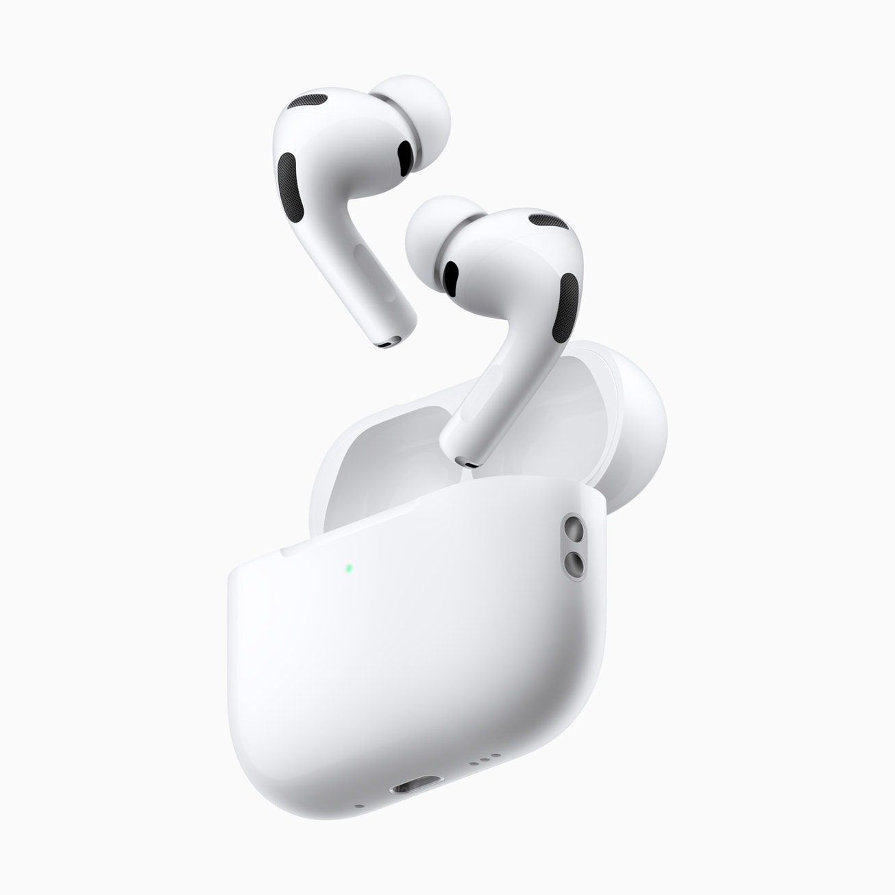