ELE Times
NANO Nuclear Energy: Pioneering Portable Microreactors and Vertically Integrated Fuel Solutions for Sustainable Power
NANO Nuclear Energy Inc. is making significant strides in the nuclear energy sector, focusing on becoming a diversified and vertically integrated company. On July 18, the company successfully closed an additional sale of 135,000 common stock shares at $20.00 per share, marking a significant financial milestone. NANO Nuclear, recognized as the first publicly listed portable nuclear microreactor company in the U.S., according to its website, is dedicated to advancing sustainable energy solutions through four main business areas: portable microreactor technology, nuclear fuel fabrication, nuclear fuel transportation, and consulting services within the nuclear industry.
NANO Nuclear is led by a team of world-class nuclear engineers who are developing cutting-edge products like the ZEUS solid core battery reactor and the ODIN low-pressure coolant reactor. These cutting-edge nuclear microreactors are engineered to provide clean, portable, and on-demand energy solutions, effectively meeting both present and future energy demands.
In a recent interview, NANO Nuclear Energy’s CEO, James Walker, outlined the company’s ambitious plans to establish a vertically integrated nuclear fuel business through its subsidiaries, Advanced Fuel Transportation Inc. (AFT) and HALEU Energy Fuel Inc. (HEF). The goal is to secure a reliable supply chain for high-assay, low-enriched uranium (HALEU) fuel, which is crucial for advanced nuclear reactors. HALEU, enriched to contain 5-19.9% of the fissile isotope U-235, enhances reactor performance, allowing for smaller designs with higher power density. Recognizing these advantages, HEF is planning to invest in fabrication facilities to meet the growing demand for advanced reactor fuel.
AFT, a key subsidiary of NANO Nuclear, is led by former executives from the world’s largest transportation companies. The subsidiary aims to establish a North American transportation network to supply commercial quantities of fuel to small modular reactors, microreactor companies, national laboratories, the military, and Department of Energy (DoE) programs. AFT’s position is strengthened by its exclusive license for a patented high-capacity HALEU fuel transportation basket, developed in collaboration with three prominent U.S. national nuclear laboratories and funded by the DoE. Concurrently, HEF is dedicated to establishing a domestic HALEU fuel fabrication pipeline to cater to the expanding advanced nuclear reactor market.
Walker acknowledged several challenges that the company faces and outlined strategies to overcome them. One of the main challenges lies in navigating the intricate regulatory landscape. Obtaining numerous permits and licenses from bodies like the Nuclear Regulatory Commission (NRC) and the DoE is essential for nuclear fuel operations. To address this, NANO Nuclear plans to invest in a dedicated regulatory affairs team to manage the licensing process and ensure ongoing compliance with stringent safety and environmental standards. Early and consistent engagement with regulators will also be crucial to align operations with regulatory expectations.
Technical and engineering challenges are also a significant focus for NANO Nuclear. Walker emphasized the importance of developing and optimizing the deconversion process to safely and efficiently handle enriched uranium hexafluoride (UF6) and convert it into other uranium fuel forms. Meeting reactor specifications requires attaining the high precision and quality essential in HALEU fuel fabrication. To overcome these challenges, NANO Nuclear intends to leverage expertise from experienced nuclear engineers and collaborate with research institutions for technology development. Rigorous quality control systems and continuous improvement practices will be key components in addressing these technical hurdles.
Another set of challenges relates to supply chain and logistics. Given the stringent safety protocols required for handling radioactive materials, ensuring the secure and safe transport of HALEU fuel is of utmost importance. Walker noted the importance of synchronizing activities across multiple facilities to avoid bottlenecks and delays. To effectively manage the supply chain, NANO Nuclear intends to establish strong transportation and security protocols in collaboration with specialized logistics companies, along with implementing advanced tracking and coordination systems.
Economic and financial viability is another critical consideration. Building facilities for deconversion, fuel fabrication, and transportation demands significant capital investment. To ensure the economic viability of the integrated supply chain, managing operational costs is essential. Walker highlighted the need to secure a range of funding sources, such as government grants, private investments, and strategic partnerships. To support these efforts, NANO Nuclear will develop detailed financial models to forecast costs and revenues and implement cost-control measures.
Market and demand uncertainties also pose challenges for the company. It is crucial to secure adequate demand for HALEU fuel, especially from microreactor manufacturers and other potential clients. To tackle this, NANO Nuclear intends to carry out market research to identify and secure long-term contracts with key customers. By differentiating its product offerings through quality, reliability, and integrated services, the company aims to compete effectively with existing fuel suppliers and new market entrants.
Addressing human resources and expertise is equally important for NANO Nuclear’s success. Recruiting and retaining highly skilled personnel with expertise in nuclear technology, engineering, and regulatory compliance is critical. To this end, Walker mentioned that the company will develop a comprehensive human resources strategy focusing on recruitment, training, and career development to ensure the necessary talent is in place.
The company’s advancements in microreactor technology are particularly noteworthy. The latest advanced microreactors, with a thermal energy output ranging from 1 to 20 megawatts, provide a flexible and portable option compared to traditional nuclear reactors. Microreactors can generate clean and reliable electricity for commercial use while also supporting a range of non-electric applications, such as district heating, water desalination, and hydrogen fuel production.
NANO Nuclear is at the forefront of this technology with its innovative ZEUS microreactor ZEUS boasts a distinctive design with a fully sealed core and a highly conductive moderator matrix for effective dissipation of fission energy. The entire core and power conversion system are housed within a single shipping container, making it easy to transport to remote locations. Engineered to deliver continuous power for a minimum of 10 years, ZEUS provides a dependable and clean energy solution for isolated areas, utilizing conventional materials to lower costs and expedite time to market.
The ZEUS microreactor’s completely sealed core design eliminates in-core fluids and associated components, significantly impacting overall system reliability and maintenance requirements. By reducing the number of components prone to failure, such as pumps, valves, and piping systems, the reactor’s design decreases the likelihood of mechanical failures and leaks, thereby enhancing overall reactor reliability. This inherently safer design also eliminates coolant loss scenarios, which are among the most severe types of reactor incidents.
With fewer moving parts, the maintenance intervals for ZEUS are significantly reduced. Components that avoid exposure to corrosive and erosive fluids have an extended service life, leading to fewer and less extensive maintenance activities. The absence of fluids simplifies inspections and replacements, making routine maintenance easier and quicker, ultimately reducing reactor downtime and operational costs.
Using an open-air Brayton cycle for power conversion in the ZEUS microreactor presents both significant benefits and challenges. The cycle’s high thermodynamic efficiency and mechanical robustness make it suitable for remote locations. By using air as the working fluid, the need for water is eliminated, reducing corrosion risk and making the reactor ideal for arid regions. However, challenges include managing high temperatures and ensuring material durability. Efficient heat exchanger design and advanced control systems are crucial, along with robust filtration and adaptable systems to handle dust and temperature extremes in remote areas.
The highly conductive moderator matrix in the ZEUS microreactor significantly enhances safety and efficiency in dissipating fission energy compared to traditional reactor designs. This advanced matrix ensures superior thermal conductivity, allowing for rapid and efficient heat transfer away from the reactor core. The matrix’s thermal properties also support passive cooling mechanisms, such as natural convection, that operate without external power, adding a critical safety layer during emergencies.
NANO Nuclear is also developing the ODIN advanced nuclear reactor to diversify its technology portfolio. The ODIN design will use conventional fuel with up to 20% enrichment, minimizing development and testing costs With its low-pressure coolant system, the design improves structural reliability and extends service life. ODIN’s high-temperature operation ensures resilient performance and high-power conversion efficiency. Utilizing natural convection for heat transfer and decay heat removal, it offers robust safety features that align with the company’s commitment to advancing nuclear technology.
In summary, NANO Nuclear Energy Inc. is pioneering advancements in nuclear energy through its focus on portable microreactor technology and a vertically integrated supply chain. The company’s innovative ZEUS and ODIN reactors, along with its strategic approach to addressing regulatory, technical, and market challenges, position it as a key player in the future of sustainable energy solutions.
The post NANO Nuclear Energy: Pioneering Portable Microreactors and Vertically Integrated Fuel Solutions for Sustainable Power appeared first on ELE Times.
Budget 24-25 calls for India-first schemes & policies to boost industries and morale of the nation
With the idea of “Viksit Bharat” in the making, the Union Budget 24-25 has brought a sense of motive and accomplishment to the social and economic fabric of the country. The compelling vision towards upskilling, research and development, employment, and women-centric opportunities seems to be a just and progressive way forward.
Not to mention, the govt. has stepped up substantially to elevate the electronics and technology industry. The intention is crystal clear and the focus is sharp. The allocation of Rs 21,936 crore to the Ministry of Electronics and Information Technology (MeitY), marks a significant 52% increase from the revised estimates of FY24, which were Rs 14,421 crore. This boost supports various incentive schemes and programs under MeitY, including semiconductor manufacturing, electronics production, and the India AI Mission.
Speaking of the ministry’s departments, the modified scheme for establishing compound semiconductors, silicon photonics, sensor fabs, discrete semiconductor fabs, and facilities for semiconductor assembly, testing, marking, and packaging (ATMP) and outsourced semiconductor assembly and testing (OSAT) received the highest allocation of Rs 4,203 crore, up from Rs 1,424 crore in FY24. Additionally, the scheme for setting up semiconductor fabs in India has been allocated Rs 1,500 crore for FY25, a big shout-out.
The production-linked incentive (PLI) scheme for large-scale electronics manufacturing also increased, with its outlay rising from Rs 4,489 crore in the revised estimates to Rs 6,125 crore for FY25. For the India AI Mission, the government has allocated Rs 511 crore for FY25.
Furthermore, the National Informatics Centre (NIC), responsible for e-governance and digital infrastructure has received an increased outlay of Rs 1,748 crore, up from Rs 1,552 crore in the previous fiscal year’s revised estimates. The substantial rise in MeitY’s budget, reaching Rs 21,936.9 crore for 2024-25, compared to Rs 14,421.25 crore for 2023-24, is largely due to the capital allocation towards the Modified Programme for Development of Semiconductors and Display Manufacturing Ecosystem in India, which saw a 355% increase to Rs 6,903 crore from Rs 1,503.36 crore in FY24.
Incentive schemes for semiconductors and large-scale electronics manufacturing, as well as IT hardware, are providing significant support to large companies like Micron and Tata Electronics to establish facilities in India. Additionally, Rs 551.75 crore has been allocated for the “India AI Mission” to enhance the country’s AI infrastructure. The previous NDA cabinet had approved over Rs 10,300 crore for the India AI Mission in March, aimed at catalyzing various components, including IndiaAI Compute Capacity, IndiaAI Innovation Centre, IndiaAI Datasets Platform, IndiaAI Application Development Initiative, IndiaAI FutureSkills, IndiaAI Startup Financing, and Safe & Trusted AI.
The other aspects of the budget concentrating on the Prime Minister’s “Vocal for Local” vision including “PM Surya Ghar Muft Bijli Yojana” among others is both timely and commendable. Overall, the budget is sure to empower the Indian spirit in action and open new growth avenues for indigenous players. I am excited to see how things will pan out for us as a nation in the next decade.
The post Budget 24-25 calls for India-first schemes & policies to boost industries and morale of the nation appeared first on ELE Times.
When did short range radio waves begin to shape our daily life?
Courtesy: u-blox
The roots of short-range wireless communicationYou arrive at your smart home after a long day. The phone automatically connects to the local network and the temperature inside is perfect, neither too cold nor too hot. As you settle into your favourite couch and plug in your headphones, ready to enjoy a good song, a family member asks you to connect your devices to share some files. While waiting, you are drawn to an old radio that once belonged to your grandmother. For a moment, everything vanishes, and you catch a glimpse into the past, imagining a distant decade when none of these short-range wireless technologies existed.
The mentioned activities require the transmission of data via radio waves traveling through the air at the speed of light. Although we cannot observe them, radio waves carry information between transmitters and receivers at different frequencies and distances. As a fundamental and ubiquitous information carrier, short-range wireless technology is now part of our daily lives. For this to happen, many scientific and technological developments had to come first.
A peek into short-range prehistoryThe electric telegraph was the first step – a revolutionary development that took shape in the first decades of the 19th century. Then, in the 1880s, Heinrich Hertz demonstrated the existence of electromagnetic waves (including radio waves), proving the possibility of transmitting and receiving electrical waves through the air. Building on Hertz’s work, Guillermo Marconi succeeded in sending a wireless message in 1895.
At the turn of the century, the application of radio waves for communication was a significant innovation. Thanks to the discovery of the radio and the development of transmitters and receivers, by the 1920s, it was possible to send messages, broadcast media, and listen to human voices and music remotely.
Radios penetrated millions of homes within just a few decades. While audio transmissions opened a new chapter in communications, visual broadcasting became the next challenge. Television quickly emerged as the next widely available communication technology.
The common denominator of these early communications and broadcasting tools was the use of high-power transmitters and radio frequency channels in the lower part of the spectrum. At the time, they were defined as long, medium, and short waves. But since the 1960s, using the specific frequency band or channel for each communication link has been more common than referring to the wavelength.
For decades, these developments focused on perfecting broadcast technologies, exploring the scope of long range communication, and reaching ever farther away places. The story didn’t stop there, though. Scientists and engineers went several steps further and began experimenting with cellular technology for mobile applications in the licensed spectrum and short range radio and wireless technologies in the license-free spectrum, opening up new personal and data communications possibilities.
The history of short range and cellular radio technology is rich. For this reason, we will focus on the former for now, while a future blog will cover the latter.
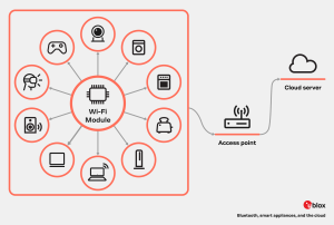
Short range radioWhen we talk about short-range wireless technologies, we refer to technologies that can communicate between devices within a range up to typically 10-30 m. Bluetooth and Wi-Fi are the most common short-range technologies. This communication is made possible by short-range wireless chips and modules embedded in smartphones and many other devices, enabling them to connect and communicate with others nearby.
Once the long-range transmission infrastructure and broadcast systems were in place, a sudden interest in short-range communications occurred about forty years ago. The expansion of the radio spectrum frequencies by the U.S. Federal Communications Commission allowed civilian devices to transmit at 900 MHz, 2.4 GHz, and 5.8 GHz. With the development of various communication technologies, the short-range wireless technology era was about to commence.
Wi-FiWe are all familiar with this term, and today, the first thing we do when we arrive at a new place, be it a friend’s house, a restaurant, or a train station, is to request the Wi-Fi password. Once your phone is ‘in,’ high-speed data transfer via radio waves begins.
What were you up to in the 1980s? While many of us were immersed in 80s culture, including fashion, music, and movies, technology companies were busy building the infrastructure for wireless local area networks (WLANs). Relying on this infrastructure, manufacturers began producing tons of devices. Soon, the incompatibility between devices from different brands led to an uncertain period that yearned for a common wireless standard.
This period came to an end with an agreement in 1997. The Institute of Electrical and Electronics Engineers released the common 802.11 standard, uniting some of the largest companies in the industry and paving the way for the Wireless Ethernet Compatibility Alliance (WECA). With the 802.11 standard, the technology soon to be known as Wi-Fi was born.
In 2000, the Wi-Fi Alliance organization continued promoting the new wireless networking technology, popularizing the term Wi-Fi (Wireless Fidelity). In the years that followed, Alliance members devoted much effort to secure applications, use cases, and interoperability for Wi-Fi products.
BluetoothAn iconic piece of technology from the 80s was the Walkman. It was everywhere and everyone loved it. Mixing your tapes to listen to music for at least an hour was like creating your favourite lists on Spotify.
Invented in the late 1970s, the Walkman was so revolutionary that it remained on the market for about 40 years, with sales peaking in the first two decades.
While highly innovative, this technology had one major drawback: the cord. When you exercised or engaged in any activity that required movement, you would inevitably get stuck or tangled in the objects around you.
The idea for Bluetooth technology originated from a patent issued in 1989 by Johan Ullman, a Swedish physician born in 1953. He obtained this patent while researching analog cordless headsets for mobile phones, possibly inspired by the inconvenience of tangled wires while using a Walkman. His work was the seed that laid the foundation for wireless headsets.
One of Ericsson’s most ambitious endeavors in the 1990s was materializing Ullman’s idea. Building upon his patent and another one from 1992, Nils Rydbeck, then CTO of Ericsson Mobile, commissioned a team of engineers led by Sven Mattisson to develop what we know today as Bluetooth technology. The innovation is captured as a modern runestone replica erected by Ericsson in Lund in 1999 in memory of Harald Bluetooth.
ThreadAlthough not defined as a short-range technology, this networking protocol is a newer tool for smart home and Internet of Things (IoT) applications. It is highly advantageous because it can provide reliable, low-power, and secure connectivity.
Thread’s origins date back to 2013, when a team at Nest Labs set out to develop a new networking protocol for smart home devices. The company had previously created an earlier version called Nest Weave. Much like the early days of Wi-Fi, this version showed a significant shortcoming: a lack of interoperability between devices from different manufacturers.
With the advent of IoT devices, the need for a specific networking protocol became evident. In 2015, the Thread Group – initially consisting of seven companies, including Samsung, and later joined by Google and Apple ‒ released the Thread Specification 1.0.
This specification defined the details of the networking protocol designed for IoT devices. Critical for manufacturers, this protocol enables the development of secure and reliable Thread-compatible devices and facilitates communication between smart devices in home environments.
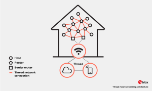
This networking protocol is unique because of its mesh networking architecture, a key differentiator. The architecture enables multiple devices, or nodes, to form a sectioned mesh network in which each device can communicate with the other members of the set. A mesh topology makes communication efficient and reliable, even when specific nodes fail or are unavailable.
Thread technology has gained traction and support over the past decade, particularly among companies developing solutions for the smart home and IoT ecosystem. Device manufacturers, semiconductor companies, software developers, and service providers all recognize the relevance of this protocol for building connected and interoperable smart home systems.
Wave me up before you go!The amount of data transmitted over the air has never been as extreme as today. Signal transmission between electronic devices has increased exponentially. Both long- and short-range waves enable transmission and communication to, from, and between devices to join networks for accessing the Internet, for instance. Now, a myriad of radio waves surrounds us.
Over the past 34 years, each of these short-range technologies (comprising the protocol) has contributed to the advancement of connectivity in various industries, including automotive, industrial automation, and many others. Until recent years, they have done so independently.
Today, the challenge for manufacturers and other stakeholders is choosing the most appropriate technology for each application, such as Bluetooth or Thread. They have also realized that combining these technologies can further advance the possibilities of IoT connectivity.
Next time you connect your smartphone to your wireless headphones, ask for the network password at a coffee shop, or communicate with colleagues on a Thread network, take a moment to remember the steps needed to live in such a connected world.
The post When did short range radio waves begin to shape our daily life? appeared first on ELE Times.
STM32CubeProgrammer 2.17 simplifies serial numbering and option byte configurations
Author : STMicroelectronics
STM32CubeProgrammer 2.17 is the very definition of a quality-of-life improvement. While it ensures support for the latest STM32s, it also brings features that will make a developer’s workflow more straightforward, such as writing ASCII strings in memory, automatic incrementation in serial numbering, or exporting and importing byte options. This new release also shows how ST listens to its community, which is why we continue to bring better support to Segger probes. In its own way, each release of STM32CubeProgrammer is a conversation we have with STM32 developers, and we can’t wait to hear what everyone has to say.
What’s new in STM32CubeProgrammer 2.17? New MCU SupportThis latest version of STM32CubeProgrammer supports STM32C0s with 128 KB of flash. It also recognizes the STM32MP25, which includes a 1.35-TOPS NPU , and all the STM32WB0s we recently released, including the STM32WB05, STM32WB05xN, STM32WB06, and STM32WB07. In the latter case, we announced their launch just a few weeks ago, thus showing that STM32CubeProgrammer keeps up with the latest releases to ensure developers can flash and debug their code on the newest STM32s as soon as possible.
New Quality-of-Life Improvements.The other updates brought on by STM32CubeProgrammer 2.17 aim to make a developer’s job easier by tailoring our utility to their workflow. For instance, we continue to build on Segger’s previous support of the J-Link and Flasher probes to ensure they support a read protection level (RDP) regression with password, thus bridging the gap between what’s possible with an STLINK probe and what’s available on the Segger models. Consequently, developers already using our partner’s probes won’t feel like they are missing out. Another update brought on by version 2.17 is the ability to generate serial numbers and automatically increment them within STM32CubeProgrammer, thus hastening the process of flashing multiple STM32s in one batch.
Other quality-of-life improvements aim to make STM32CubeProgrammer more intuitive. For instance, it is now possible to export an STM32’s option bytes. Very simply, they are a way to store configuration options, such as read-out protection levels, watchdog settings, power modes, and more. The MCU loads them early in the boot process, and they are stored in a specific part of the memory that’s only accessible by debugging tools or the bootloader. By offering the ability to export and import option bytes, STM32CubeProgrammer enables developers to configure MCUs much more easily. Similarly, version 2.17 can now edit memory fields in ASCII to make certain section a lot more readable.
What is STM32CubeProgrammer? An STM32 flasher and debuggerAt its core, STM32CubeProgrammer helps debug and flash STM32 microcontrollers. As a result, it includes features that optimize these two processes. For instance, version 2.6 introduced the ability to dump the entire register map and edit any register on the fly. Previously, changing a register’s value meant changing the source code, recompiling it, and flashing the firmware. Testing new parameters or determining if a value is causing a bug is much simpler today. Similarly, engineers can use STM32CubeProgrammer to flash all external memories simultaneously. Traditionally, flashing the external embedded storage and an SD card demanded developers launch each process separately. STM32CubeProgrammer can do it in one step.
Another challenge for developers is parsing the massive amount of information passing through STM32CubeProgrammer. Anyone who flashes firmware knows how difficult it is to track all logs. Hence, we brought custom traces that allow developers to assign a color to a particular function. It ensures developers can rapidly distinguish a specific output from the rest of the log. Debugging thus becomes a lot more straightforward and intuitive. Additionally, it can help developers coordinate their color scheme with STM32CubeIDE, another member of our unique ecosystem designed to empower creators.
 STM32CubeProgrammer
What are some of its key features?
New MCU support
Most new versions of STM32CubeProgrammer support a slew of new MCUs. For instance, version 2.16 brought compatibility with the 256 KB version of the STM32U0s. The device was the new ultra-low power flagship model for entry-level applications thanks to a static power consumption of only 16 nA in standby. STM32CubeProgrammer 2.16 also brought support for the 512 KB version of the STM32H5, and the STM32H7R and STM32H7S, which come with less Flash so integrators that must use external memory anyway can reduce their costs. Put simply, ST strives to update STM32CubeProgrammer as rapidly as possible to ensure our community can take advantage of our newest platforms rapidly and efficiently.
SEGGER J-Link probe supportTo help developers optimize workflow, we’ve worked with SEGGER to support the J-Link probe fully. This means that the hardware flasher has access to features that were previously only available on an ST-LINK module. For instance, the SEGGER system can program internal and external memory or tweak the read protection level (RDP). Furthermore, using the J-Link with STM32CubeProgrammer means developers can view and modify registers. We know that many STM32 customers use the SEGGER probe because it enables them to work with more MCUs, it is fast, or they’ve adopted software by SEGGER. Hence, STM32CubeProgrammer made the J-Link vastly more useful, so developers can do more without leaving the ST software.
Automating the installation of a Bluetooth LE stackUntil now, developers updating their Bluetooth LE wireless stack had to figure out the address of the first memory block to use, which varied based on the STM32WB and the type of stack used. For instance, installing the basic stack on the STM32WB5x would start at address 0x080D1000, whereas a full stack on the same device would start at 0x080C7000, and the same package starts at 0x0805A000 on the STM32WB3x with 512 KB of memory. Developers often had to find the start address in STM32CubeWB/Projects/STM32WB_Copro_Wireless_Binaries. The new version of STM32CubeProgrammer comes with an algorithm that determines the right start address based on the current wireless stack version, the device, and the stack to install.
A portal to security on STM32Readers of the ST Blog know STM32CubeProgrammer as a central piece of the security solutions present in the STM32Cube Ecosystem. The utility comes with Trusted Package Creator, which enables developers to upload an OEM key to a hardware secure module and to encrypt their firmware using this same key. OEMs then use STM32CubeProgrammer to securely install the firmware onto the STM32 SFI microcontroller. Developers can even use an I2C or SPI interface, which gives them greater flexibility. Additionally, the STM32H735, STM32H7B, STM32L5, STM32U5, and STM32H5 also support external secure firmware install (SFIx), meaning that OEMs can flash the encrypted binary on memory modules outside the microcontroller.
Secure ManagerSecure Manager is officially supported since STM32CubeProgrammer 2.14 and STM32CubeMX 1.13. Currently, the feature is exclusive to our new high-performance MCU, the STM32H573, which supports a secure ST firmware installation (SSFI) without requiring a hardware secure module (HSM). In a nutshell, it provides a straightforward way to manage the entire security ecosystem on an STM32 MCU thanks to binaries, libraries, code implementations, documentation, and more. Consequently, developers enjoy turnkey solutions in STM32CubeMX while flashing and debugging them with STM32CubeProgrammer. It is thus an example of how STM32H5 hardware and Secure Manager software come together to create something greater than the sum of its parts.
Other security features for the STM32H5STM32CubeProgrammer enables many other security features on the STM32H5. For instance, the MCU now supports secure firmware installation on internal memory (SFI) and an external memory module (SFIx), which allows OEMs to flash encrypted firmware with the help of a hardware secure module (HSM). Similarly, it supports certificate generation on the new MCU when using Trusted Package Creator and an HSM. Finally, the utility adds SFI and SFIx support on STM32U5s with 2 MB and 4 MB of flash.
Making SFI more accessible The STM32HSM used for SFI with STM32CubeProgrammer
Since version 2.11, STM32CubeProgrammer has received significant improvements to its secure firmware install (SFI) capabilities. For instance, in version 2.15, ST added support for the STM32WBA5. Additionally, we added a graphical user interface highlighting addresses and HSM information. The GUI for Trusted Package Creator also received a new layout under the SFI and SFIx tabs to expose the information needed when setting up a secure firmware install. The Trusted package creator also got a graphical representation of the various option bytes to facilitate their configuration.
Secure secret provisioning for STM32MPxSince 2.12, STM32CubeProgrammer has a new graphical user interface to help developers set up parameters for the secure secret provisioning available on STM32MPx microprocessors. The mechanism has similarities with the secure firmware install available on STM32 microcontrollers. It uses a hardware secure module to store encryption keys and uses secure communication between the flasher and the device. However, the nature of a microprocessor means more parameters to configure. STM32CubeProgrammers’ GUI now exposes those settings previously available in the CLI version of the utility to expedite workflows.
Double authenticationSince version 2.9, the STM32CubeProgrammer supports a double authentication system when provisioning encryption keys via JTAG or a Boot Loader for the Bluetooth stack on the STM32WB. Put simply, the feature enables makers to protect their Bluetooth stack against updates from end-users. Indeed, developers can update the Bluetooth stack with ST’s secure firmware if they know what they are doing. However, a manufacturer may offer a particular environment and, therefore, may wish to protect it. As a result, the double authentication system prevents access to the update mechanism by the end user. ST published the application note AN5185 to offer more details.
PKCS#11 supportSince version 2.9, STM32CubeProgrammer supports PKCS#11 when encrypting firmware for the STM32MP1. The Public-Key Cryptography Standards (PKCS) 11, also called Cryptoki, is a standard that governs cryptographic processes at a low level. It is gaining popularity as APIs help embedded system developers exploit its mechanisms. On an STM32MP1, PKCS#11 allows engineers to segregate the storage of the private key and the encryption process for the secure secret provisioning (SSP).
SSP is the equivalent of a Secure Firmware Install for MPUs. Before sending their code to OEMs, developers encrypt their firmware with a private-public key system with STM32CubeProgrammer. The IP is thus unreadable by third parties. During assembly, OEMs use the provided hardware secure module (HSM) containing a protected encryption key to load the firmware that the MPU will decrypt internally. However, until now, developers encrypting the MPU’s code had access to the private key. The problem is that some organizations must limit access to such critical information. Thanks to the new STM32CubeProgrammer and PKCS#11, the private key remains hidden in an HSM, even during the encryption process by the developers.
Supporting new STM32 MCUs Access to the STM32MP13’s bare metalMicrocontrollers demand real-time operating systems because of their limited resources, and event-driven paradigms often require a high level of determinism when executing tasks. Conversely, microprocessors have a lot more resources and can manage parallel tasks better, so they use a multitasking operating system, like OpenSTLinux, our Embedded Linux distribution. However, many customers familiar with the STM32 MCU world have been asking for a way to run an RTOS on our MPUs as an alternative. In a nutshell, they want to enjoy the familiar ecosystem of an RTOS and the optimizations that come from running bare metal code while enjoying the resources of a microprocessor.
Consequently, we are releasing today STM32CubeMP13, which comes with the tools to run a real-time operating system on our MPU. We go into more detail about what’s in the package in our STM32MP13 blog post. Additionally, to make this initiative possible, ST updated its STM32Cube utilities, such as STM32CubeProgrammer. For instance, we had to ensure that developers could flash the NOR memory. Similarly, STM32CubeProgrammer enables the use of an RTOS on the STM32MP13 by supporting a one-time programmable (OTP) partition.
Traditionally, MPUs can use a bootloader, like U-Boot, to load the Linux kernel securely and efficiently. It thus serves as the ultimate first step in the boot process, which starts by reading the OTP partition. Hence, as developers move from a multitasking OS to an RTOS, it was essential that STM32CubeProgrammer enable them to program the OTP partition to ensure that they could load their operating system. The new STM32CubeProgrammer version also demonstrates how the ST ecosystem works together to release new features.
STM32WB and STM32WBA supportSince version 2.12, STM32CubeProgrammer has brought numerous improvements to the STM32WB series, which is increasingly popular in machine learning applications, as we saw at electronica 2022. Specifically, the ST software brings new graphical tools and an updated wireless stack to assist developers. For instance, the tool has more explicit guidelines when encountering errors, such as when developers try to update a wireless stack with the anti-rollback activated but forget to load the previous stack. Similarly, new messages will ensure users know if a stack version is incompatible with a firmware update. Finally, STM32CubeProgrammer provides new links to download STM32WB patches and get new tips and tricks so developers don’t have to hunt for them.
Similarly, STM32CubeProgrammer supports the new STM32WBA, the first wireless Cortex-M33. Made official a few months ago, the MCU opens the way for a Bluetooth Low Energy 5.3 and SESIP Level 3 certification. The MCU also has a more powerful RF that can reach up to +10 dBm output power to create a more robust signal.
STM32H5 and STM32U5The support for STM32H5 began with STM32CubeProgrammer 2.13, which added compatibility with MCUs, including anything from 128 KB up to 2 MB of flash. Initially, the utility brought security features like debug authentication and authentication key provisioning, which are critical when using the new life management system. The utility also supported key and certificate generation, firmware encryption, and signature. Over time, ST added support for the new STM32U535 and STM32U545 with 512 KB and 4 MB of flash. The MCUs benefit from RDP regression with a password to facilitate developments and SFI secure programming.
Additionally, STM32CubeProgrammer includes an interface for read-out protection (RDP) regression with a password for STM32U5xx. Developers can define a password and move from level 2, which turns off all debug features, to level 1, which protects the flash against certain reading or dumping operations, or to level 0, which has no protections. It will thus make prototyping vastly simpler.
STLINK-V3PWRIn many instances, developers use an STLINK probe with STM32CubeProgrammer to flash or debug their device. Hence, we quickly added support for our latest STLINK-PWR probe, the most extensive source measurement unit and programmer/debugger for STM32 devices. If users want to see energy profiles and visualize the current draw, they must use STM32CubeMonitor-Power. However, STM32CubeProgrammer will serve as an interface for all debug features. It can also work with all the probe’s interfaces, such as SPI, UART, I2C, and CAN.
Script modeThe software includes a command-line interface (CLI) to enable the creation of scripts. Since the script manager is part of the application, it doesn’t depend on the operating system or its shell environment. As a result, scripts are highly sharable. Another advantage is that the script manager can maintain connections to the target. Consequently, STM32CubeProgrammer CLI can keep a connection live throughout a session without reconnecting after every command. It can also handle local variables and even supports arithmetic or logic operations on these variables. Developers can thus create powerful macros to automate complex processes. To make STM32CubeProgrammer CLI even more powerful, the script manager also supports loops and conditional statements.
A unifying experienceSTM32CubeProgrammer aims to unify the user experience. ST brought all the features of utilities like the ST-LINK Utility, DFUs, and others to STM32CubeProgrammer, which became a one-stop shop for developers working on embedded systems. We also designed it to work on all major operating systems and even embedded OpenJDK8-Liberica to facilitate its installation. Consequently, users do not need to install Java themselves and struggle with compatibility issues before experiencing STM32CubeProgrammer.
Qt 6 supportSince STM32CubeProgrammer 2.16, the ST utility uses Qt 6, the framework’s latest version. Consequently, STM32CubeProgrammer no longer runs on Windows 7 and Ubuntu 18.04. However, Qt 6 patches security vulnerabilities, brings bug fixes, and comes with significant quality-of-life improvements.
The post STM32CubeProgrammer 2.17 simplifies serial numbering and option byte configurations appeared first on ELE Times.
How Synopsys IP and TSMC’s N12e Process are Driving AIoT
Hezi Saar | Synopsys
Artificial intelligence (AI) is revolutionizing nearly every aspect of our lives in all industries, driving the transformation of technology from development to consumption and reshaping how we work, communicate, and interact. On the other hand, the Internet of Things (IoT) connects everyday objects to the internet, enabling a network of interconnected devices that adds additional improved efficiency and enhanced convenience in our lives.
The union of AI and IoT, known as AIoT, integrates AI capabilities into IoT devices and is further poised to change our lives and drive the semiconductor industry’s expansion in the foreseeable future. AIoT devices can analyze and interpret data in real-time, enabling smart decisions, autonomously adapting to observed conditions. Promising heightened intelligence, connectivity, and device interactivity, AIoT is capable of handling vast data volumes without needing to rely on cloud-based processing methods.
Within AIoT devices, AI seamlessly integrates into infrastructure components, including programs and chipsets, all interconnected via IoT networks. From smart cities to smart homes and industrial automation, AIoT applications require real-time data processing that is powered by high-capacity on-chip memories, compute power, and minimal power consumption.
Read on to learn more about the opportunities and challenges of AIoT applications at the edge as well as Synopsys IP on TSMC’s N12e process and how it supports pervasive AI at the edge.
AIoT Applications at the EdgeAI is truly everywhere and can be found in data centers, cars, and high-end compute devices. However, processing data at or close to the source of information complements the cloud-based AI approach and allows for the immediate processing of data and speedy results for optimal service, more personalized functions to the user, protection of information/additional privacy, and additional reliability.
Everything from smartwatches, security cameras, smart fridges, automation-enabled factory machinery, smart traffic lights, and more are considered AIoT devices. Each of these devices is unique in some way which requires chip designers to find the right balance between performance, power usage, and cost.
For an application like smart cities, low power is the much bigger factor (although performance can’t be completely ignored). For example, think about a smart streetlamp with sensing capabilities that are programmed to come on at sunset and sunrise. With an average streetlamp measuring around 30 feet tall, changing out a burnt-out light bulb and any other components becomes a larger, costlier, and more time-consuming task. Also, controlling the time the lights are on at night at a lower strength creates a more cost-effective as well as environmentally friendly approach, and reduces the light pollution that these streetlamps usually cause. That’s why designing these smart devices to take up as little power as possible for years of use is so important; it extends the life of the streetlamp and enables a smart City environment.
Additionally, minimizing power consumption naturally leads to a smaller cost, size, and weight. It can also help to maximize the user experience, increase the silicon reliability, maximize the lifespan of the IoT device, and lessen environmental impact. Overall, AIoT applications are driving demand for high-performance and low-latency memory interfaces on low leakage nodes.
AIoT Products and Their Corresponding Power-Saving ApproachMany different power-saving approaches can be built into the IP and, ultimately, the chip depending on how the AIoT device is charged.
- Battery-Powered: Sensors that detect water, fire/smoke, intruders, etc. are idle until the alarm/camera/Wi-fi trigger is detected. Many times, the entire sensor needs to be replaced after the job is finished. External power gating (read more on that below) is the best solution. Other battery-powered applications such as door locks and key fobs allow for battery replacement and may require USB 1.1/2.0 connectivity with a power island from Vbus, and NVM.
- Battery-Powered with Energy Harvesting: Examples of this type might include doorbells, security cameras, environment sensors, price tagging, remote controls, and more. MAC IIP opportunities to address these products involve CSI for Camera, M-PHY or eMMC for storage, SPI/PCIe for Wi-Fi, DSI for display, and USB 2.0 for advanced products to assist with charging and firmware download.
- Portable: Users charge these products when/if needed based on use-case. For instance, wearables, personal infotainment devices, audio headsets, e-readers, etc. need to be charged every few days to several weeks depending on how often they are used. For other devices like laptops and phones, it is mandatory to save power when they are not connected to an external power source. This means requiring a fast sleep/resume and power gating if applicable.
- Stationary: Devices that facilitate home networking, home automation, and security, as well as home hubs like Alexa Echo Show or Google Nest are either powered most of the time in a docking station or need to be plugged in all the time with battery backup for keeping settings. The ability to fast sleep/resume and DVFS are both useful for saving power.
The semiconductor industry has considered 16nm and 12nm “long nodes” (or nodes that will be around for many, many years to come) for consumer, IoT, wireless, and certain automotive applications. These nodes can leverage AI because they have great performance using the FinFet process but are also cost-effective and low power.
TSMC has made investments to boost performance and power in these nodes, making them even more appealing for power-conscious designs. For example, N12e offers a device boost for higher density with good performance/power tradeoffs and ultra-low leakage static random-access memory (SRAMs).
Not only does this provide approximately 15% power savings and the memory required to process all that data at the edge, but it is also compatible with existing design rules to minimize IP investment. That’s where Synopsys comes in.
Synopsys IP reduces leakage even further through a variety of different techniques:
- Power Gating: This technique can be used from an active state or a disabled or “turned-off state.” An active state requires retention/restoring such that it is possible to save the state the IP is currently at once power gating is exited. To use this mode, circuits such as always-on domain retention and power control logic are required. Entering power gating from a disabled state requires IP that supports power collapsing and needs to be restarted after power gating is exited.
- Voltage Scaling: IP is also available to scale the voltage down in order to reduce the leakage consumption. There are two types of voltage scaling — dynamic voltage and frequency scaling. With frequency scaling, IP is still performing functional activities but the voltage is reduced in order to meet timing requirements.
- Retention: In this technique, voltage is reduced to a level where registers still hold their current value but it is expected that the IP is not performing functional activity. This means that there is no toggling, IDLE mode, or setup/hold sign-off.
The IP used to design AIoT chips must be versatile in order to support the many different use cases and applications that are powered by N12e process and other low power nodes. Higher-performance chips require a more sophisticated low-power strategy using the various techniques described above.
As AIoT devices become even more prevalent in our homes, workplaces, and cities, Synopsys and TSMC will continue to develop even more sophisticated high-performance, low-power solutions to fuel further innovation in this space.
The post How Synopsys IP and TSMC’s N12e Process are Driving AIoT appeared first on ELE Times.
Highlighting and Addressing the Dangers of Electric Cars
Courtesy: Revolutionized
As moving away from gas-powered vehicles becomes a more accessible option, some people wonder about the dangers of electric cars and whether those issues should discourage them from making the switch. First, consumers must remember that nothing they purchase, use or do in life is completely risk-free.
Driving an electric car is not automatically more dangerous than using one that runs on gas. Both types have associated risks that people can mitigate by taking the necessary precautions after learning about them.
Fires in Enclosed SpacesThe individual cells in EV batteries can experience thermal runaway events, leading to fires and explosions. Short circuits trigger these problems, resulting from battery damage, improper charging habits and poor maintenance.
In this regard, some of the primary dangers of electric cars relate to blazes in enclosed spaces, such as underground parking garages. Researchers are eager to learn more about what happens when those fires occur and how people should reduce the risks.
One Austrian study investigated electric car fires and their effects. A main takeaway was that the potential risks were not significantly more critical than those associated with combustion engine vehicles. However, the research also indicated that the fire-related dangers of electric cars are highest in indoor, multilevel parking garages.
The researchers also identified the need to gather additional information about commercial-grade battery-electric vehicles, such as buses. Their work involved intentionally setting the cars on fire and using 30 temperature sensors to determine how quickly the blazes released heat. Those efforts showed the warmth in the area was still safe enough for firefighters to attend to the matter.
However, that changed when the entire battery was simultaneously and fully on fire. In such cases, the heat release spiked noticeably over a few minutes, suggesting first responders must carefully monitor the fire’s state and progression when tending to it.
Additionally, this research assessed the amount of toxic gasses emitted during these events. Although those involved found comparably higher levels of hydrogen fluoride and carbon monoxide associated with EV fires, one fortunate aspect was that the most significant concentrations floated up beyond the level of those putting out the blazes. That finding kept humans safer and meant the gasses did not block potential escape routes.
Real-Life ConcernsUnfortunately, these dangers of electric cars are not hypothetical. The fires can also spread to nearby vehicles, quickly creating larger issues. One example happened at an airport, where an EV caught on fire, spreading the flames to four other surrounding automobiles.
However, it is also important to remember that these fires are not unique dangers of electric cars. A strong case for that assertion involves the 2023 incident at London Luton airport that affected 1,500 vehicles. However, investigations determined that everything started with a diesel-powered car.
There’s also a related danger, seemingly brought about by people not understanding that electric vehicle fires are relatively rare. One father posted on social media that he was forbidden to park his EV in a hospital garage when taking his child for an appointment. A security guard told him the vehicle could explode and that none were allowed in that garage until a sprinkler system upgrade occurred.
Hospital representatives later released a statement clarifying that EV owners could still use the facility’s main parking area but not the one the parent had tried to enter. However, an image circulated showing an entrance sign reading, “NO ELECTRIC VEHICLES,” with no mention that they would eventually be allowed in the garage. That approach conveys the idea that the hospital is wholly against them without a specified reason
In any case, the people who must primarily concern themselves with these blazes are those tasked with putting them out. EV fires have specific characteristics that prevent firefighters from dealing with them the same ways they would if other vehicles were ablaze. The more professionals learn about these details and keep their knowledge current, the better protected they are from these dangers of electric cars.
Isolated Charging PointsThe United States had more than 160,000 places to charge electric vehicles as of 2023. However, some people are concerned about more than the number. They also want to replenish their cars’ batteries in places that make them feel safe.
One woman in the United Kingdom experienced this during a 300-mile round trip and had to drive to several charging points before finding one that made her feel safe. The others visited before the one she ultimately chose were poorly lit, had little to no activity from other people and were not always staffed. Her challenges led her to start a business, ChargeSafe, which rates six charging station aspects on a five-point scale.
She also asserts that even one bad experience while charging an electric vehicle is too many. Indeed, some people — particularly females or those traveling alone — may resist stopping at specific stations that seem too risky. Such circumstances are often less common for gas stations, since many operate 24/7 and are almost always lit thoroughly.
A Potential Purchase BarrierMany humans dislike changes, and switching to an EV is a significant one for most. Gas-powered cars have become so embedded in modern society that some people would rather keep using them due to their familiarity. However, research also suggests that — among women — the lack of safe places to charge their vehicles could make them hesitate to purchase these options.
The study got perspectives from females in the United States and Canada, examining how charging stations influenced their overall feelings about owning EVs. The results indicated 43% of those in the United States and 30% in Canada had safety-related concerns.
Moreover, 40% of U.S. women said accessible, well-lit charging stations in well-populated areas would influence their vehicle purchasing decisions. The same was true for nearly half of the Canadians. Relatedly, 21% of those in the U.S. and 20% of Canadian respondents indicated tighter charging station security would positively impact their purchasing choices.
Addressing the Dangers of Electric CarsWhereas people interested in EV ownership commonly research range, prices and charger availability, the things on their minds won’t necessarily include the matters covered here. However, awareness is the first step to causing or supporting positive change.
Those who already have electric cars should always follow the manufacturer’s instructions for charging the battery. Additionally, they should get batteries checked for physical damage after even slight incidents that may have caused it. Those two simple but proactive measures can reduce the chances of thermal runaway events.
From a charging safety perspective, people should pay attention to related infrastructure updates in places where they live or frequently travel, advocating for EV charging stations to be in well-lit, populated locations that appear inviting and safe.
The post Highlighting and Addressing the Dangers of Electric Cars appeared first on ELE Times.
Big Future in a Small Space: Wireless SoCs Enable Wearable Medical and Wellness Devices to Realize Their Potential
Courtesy: Renesas
The technology of personal medical monitoring is changing incredibly fast. As little as ten years ago, the normal way that a patient would keep track of general health indicators, such as heart rate and blood pressure, or specific indicators such as blood glucose, was through an invasive medical procedure such as a blood test. Such testing would often need to take place away from the home, in a local clinic or a hospital.
Fast forward to today, and patients have it much better. Anyone – not just those receiving treatment from a medical practitioner – can benefit from monitoring vital signs, as well as other indicators of long-term health such as activity and sleep. That’s because a new generation of wearable medical and consumer devices have extraordinary sensor and data processing capabilities built into them. The newest types of products, such as continuous glucose monitors (CGM) and smart rings, can report on the wearer’s condition 24/7, yet are so small and light that the user is hardly aware of them, and are so convenient and easy to use that they are valuable to anyone.
At the heart of this new type of wearable medical device is advanced wireless connectivity technology: a Bluetooth Low Energy system-on-chip (SoC) for linking to a smartphone, tablet or personal computer, and NFC – the technology that enables contactless payment – for authentication, pairing, configuration, and charging.
Long Battery Life, Tiny Form FactorThe most important limits on the design of both a CGM and a smart ring are the same: space and power. Both devices perform monitoring 24/7, and the expectation is for long battery life, to limit the number of times that the user has to charge them. This puts a strong emphasis on the need for low power consumption in the wireless SoC, both in active and standby modes.
The size of the device is also a critical design parameter; its form factor has to be comfortable for all-day wearing, yet the manufacturer will be eager to pack as much functionality into the device as possible, to increase its value to the user. So this kind of wearable device requires wireless systems for connectivity and charging that are themselves small, and that require the use of the fewest number of external components, to keep the total board footprint to a minimum.
At the same time, these devices perform a range of sophisticated connectivity functions to support both local and remote data access. Despite the size and power constraints, their Bluetooth Low Energy SoC has to provide a robust and reliable connection to the user’s smartphone for data processing and analysis locally or in the cloud. And, NFC connectivity supports functions such as authentication of accessories and usage tracking as well as wireless charging. High performance is therefore an essential requirement.
This presents a tough challenge to the product designer. But manufacturers have a solution that is readily available to them: connectivity products from Renesas that save space and consume amazingly little power.
Performance and Low Power for CGM DesignsA typical example is the DA1453x series of Bluetooth SoCs, which combine very low power consumption with high integration, reducing the number of external components on the board and so saving space in CGM designs.
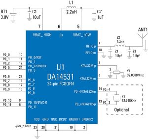
For example, the Bluetooth 5.1 DA14531 is available in a tiny 2.0mm x 1.7mm package, half the size of any offering from other leading manufacturers. On top of this, it only requires six external passive components and operates with a single crystal for timing input.
Record low hibernation and active power consumption ensure long operating and shelf life with even the smallest disposable batteries: the DA14531 is compatible with alkaline, silver oxide, and coin cell batteries, and includes an internal buck-boost DC/DC converter to extend the useful life of these battery types.
This combination of small size and very low power consumption makes the DA1453x SoCs ideal for a CGM, a small wearable device that has to perform 24/7 monitoring.
Smart Ring Designs: Multiple Functions in One Low-Power ChipRenesas Bluetooth SoCs such as the DA14695 or DA1459x are striking examples of the twin benefits of low power consumption and high integration for smart rings. The DA14695 SoC is based on a 96MHz Arm Cortex-M33F CPU core to run application functions such as processing signals from a smart ring alongside a 96MHz Cortex-M0+ core operating as a sensor node controller and configurable media access controller for the on-board Bluetooth Low Energy v5.2 radio.
The DA14695 offers a remarkable level of integration: on-chip features include a power management IC (PMIC), USB interface and USB charger, motor driver for haptic feedback, and a parallel interface driver for a display screen, as well as strong security protection. Yet in Deep Sleep mode, this high-performance device draws just 10µA.
Contrast this with other Bluetooth SoCs on the market which might provide a CPU, a protocol engine, and a sensor node controller but lack many of the peripheral capabilities in the DA14695, leading to a significant increase in the cost of components and in the amount of space required on the PCB.
Designers of smart rings and other wearable devices can use this type of Renesas Connectivity Solutions product to meet their toughest design requirements.
All-in-One Charger and Data Exchange ComponentA similar approach to power and space saving is enabled by Renesas’ NFC technology. NFC is best known for its use in contactless payment terminals, enabling a smartphone or smartwatch to securely exchange data packets to authorize a financial transaction.
In a smart ring, this data exchange capability can also be used for contactless payments. But the same PTX30W NFC tag used for data exchange also enables NFC wireless charging.
Here again, Renesas has performed a miracle of integration to save space: the PTX30W packs an NFC tag, rectifier, limiter, battery charger circuit, and a dedicated core to handle the NFC wireless charging protocol in a miniature 1.78mm x 1.78mm WLCSP package.
The PTX30W pairs with the Renesas PTX130W, a dedicated NFC charging transmitter, called a poller, embedded in the smart ring’s charging case. The PTX130W provides for the maximum power transfer and fast charging thanks to its direct antenna connection technology (DiRAC). This technology also makes the PTX130W simpler to implement in a charging case design than competing products, as it eliminates the need for EMC filters, and eases antenna matching. The superior RF performance of the PTX130W enables the use of a small antenna and allows for flexible placement of the poller’s and listener’s antennas.
By eliminating the need for additional components, and enabling the use of a small antenna, the PTX30W provides a solution for charging which can be fitted onto the tiny PCB in a smart ring such as the Ring One from Muse Wearables.
A Renesas Ecosystem for Fast and Efficient Product DevelopmentHigh performance and seamless integration are watchwords of the Renesas Connectivity Solutions portfolio, which dovetails perfectly with the Renesas line of microcontrollers and applications processors. The portfolio also gives users access to the unparalleled suite of tools and resources available from Renesas for development, including the e² studio integrated development environment, Flexible Software Package (FSP) bundles for firmware, development kits, and Winning Combinations – pre-vetted sets of compatible components for specific product designs.
The post Big Future in a Small Space: Wireless SoCs Enable Wearable Medical and Wellness Devices to Realize Their Potential appeared first on ELE Times.
Qualcomm Linux sample apps – building blocks for AI inference and video in IoT applications (Part 1 of 2)
Courtesy: Qualcomm
Qualcomm Linux sample apps – building blocks for AI inference and video in IoT applications (Part 1 of 2)In this post we’ll explore the first two building-block applications.
1. Multi-camera streamingThe command-line application gst-multi-camera-example demonstrates streaming from two camera sensors simultaneously. It can apply side-by-side composition of the video streams to show on a display device, or it can encode and store the streams to files.
The application pipeline looks like this:
The application supports two configurations:
- Composition and display – The qtimmfsrc plugin on camera 0 and camera 1 capture the data from the two camera sensors. qtivcomposer performs the composition, then waylandsink displays the streams side by side on the screen.
- Video encoding – The qtimmfsrc plugin on camera 0 and camera 1 captures the data from the two camera sensors and passes it to the v4l2h264enc plugin. The plugin encodes and compresses the camera streams to H.264 format, then hands them off for parsing and multiplexing using the h264parse and mp4mux plugins, respectively. Finally, the streams are handed off to the filesink plugin, which saves them as files.
Here’s an example of the output from the first configuration: Right side image is monochrome, as second camera sensor on development kit is monochrome.
When would you use this application?gst-multi-camera-example is a building block for capturing data from two camera sensors, with options for either composing and displaying the video streams or encoding and storing the streams to files. You can use this sample app as the basis for your own camera capture/encoding applications, including dashcams and stereo cameras.
2. Video wall – Multi-channel video decode and displayThe command-line application gst-concurrent-videoplay-composition facilitates concurrent video decode and playback for AVC-coded videos. The app performs composition on multiple video streams coming from files or the network (e.g., IP cameras) for display as a video wall.
The application can take multiple (such as 4 or 8) video files as input, decode all the compressed videos, scale them and compose them as a video wall. The application requires at least one input video file, in MP4 format with an AVC codec.
The application pipeline looks like this for 4 channels:
Each channel uses plugins to perform the following processing:
- Reads compressed video data from a file using filesrc.
- Demultiplexes the file with qtdemux.
- Parses H.264 video streams using h264parse.
- Decodes the streams using v4l2h264dec.
- The decoded streams from all channels are then composed together using qtivcomposer and displayed using waylandsink.
Here’s an example of using the app gst-concurrent-videoplay-composition on 4 video streams:
When would you use this application?With gst-concurrent-videoplay-composition you can decode multiple compressed video streams, then compose them into a video wall; for example, in retail spaces and digital signage. As an edge box for video surveillance, you can capture input from multiple IP cameras and display it in a single screen. In a video conferencing application, you can process and display feeds from multiple people on the call, with each participant streaming a video.
The post Qualcomm Linux sample apps – building blocks for AI inference and video in IoT applications (Part 1 of 2) appeared first on ELE Times.
Powering the Future of IoT: The Role of 5G RedCap in Expanding Device Connectivity
The global adoption of 5G wireless networks has been slower than anticipated, with high costs, limited coverage, and the lack of necessity for some advanced features contributing to this lag. However, the introduction of the Reduced Capability (RedCap) standard by the 3rd Generation Partnership Project (3GPP) in 2021 aims to accelerate 5G’s expansion into new markets, including industrial, medical, home and buildings, and security sectors.
What is 5G RedCap?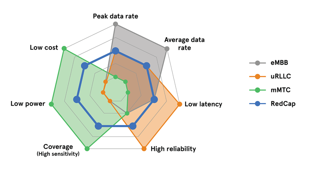 5G relies on three main pillars all running inside the 5G Core: enhanced Mobile Broadband (eMBB), ultra-Reliable Low Latency Communication (uRLLC) and massive Machine Type Communication (mMTC). 5G RedCap addresses applications that fall between these extremes. (Source: 3GPP)
5G RedCap, also known as 5G NR-Light or New Radio-Lite, is a simplified version of the 5G standard that bridges the gap between 4G and 5G. It is designed for use cases with minimal hardware requirements, where ultra-high data rates, ultra-low latency, or extremely low power are not essential, but reliable throughput is still necessary. RedCap devices are less complex and more cost-effective compared to baseline 5G devices defined by the 5G Release 15 standard.
One of the key features of RedCap devices is their ability to operate with a single receiving antenna, which reduces complexity and integration costs. These devices also incorporate low-power features like radio resource management (RRM) relaxation and extended Discontinuous Reception Mode (eDRX). These enhancements are particularly advantageous for applications involving static objects or devices that primarily upload data to the cloud, as they can significantly benefit from the resulting power savings.
Looking ahead, Enhanced Reduced Capability (eRedCap) is set to build on the benefits of RedCap by offering even smaller throughput while utilizing the same 5G standalone (SA) network.
5G RedCap: The Next Step Beyond LTE for IoT Connectivity5G RedCap and its enhanced version, eRedCap, represent the future of mid-end cellular IoT connectivity. These technologies are poised to replace LTE Cat 4 and LTE Cat 1 in the coming years, offering a more efficient solution for industrial, medical, and automotive markets that demand longevity. While it may be too early to discuss the phasing out of 4G, it is clear that from a cellular network and chipset perspective, further evolutions of 4G are unlikely.
RedCap increases the addressable 5G market by providing a functional middle ground between high-performance 5G and low-end cellular communication technologies like LTE-M and NB-IoT. Some use cases are already well-served by LTE, but new opportunities are emerging that are better suited to RedCap’s capabilities.
5G RedCap Set to Capture 18% of IoT Market by 2030The market potential for 5G RedCap is significant, particularly in regions where cost is a critical factor for the widespread adoption of digital technologies. According to the Global Cellular IoT Module Forecast, 5G RedCap modules are projected to represent 18% of all cellular IoT module shipments by 2030. This projection highlights the growing importance of RedCap technology, especially in developing nations.
5G RedCap is specifically designed to address emerging use cases that are not adequately served by existing advanced 5G standards, such as NB-IoT, Cat-M1, and 4G. With chipsets already available, 5G RedCap is poised for growth, offering reduced data flow and dependable connectivity while optimizing power consumption to significantly extend device battery life.
The flexibility and network advantages of 5G RedCap, including lower latency, higher speeds, and improved power efficiency compared to previous LTE generations, position it as a superior choice for future mass IoT deployments.
5G RedCap Powers Wearables, Surveillance, Medical Devices, and Industrial IoT: Use Cases5G RedCap is ideally suited for a diverse array of IoT applications, such as:
- Smart Wearables: Devices like smartwatches and low-end XR glasses can benefit from RedCap’s balance of performance and power efficiency.
- Video Surveillance: RedCap’s reliable connectivity and higher data rates are ideal for video surveillance applications.
- Medical Devices: Health monitors and other medical devices can leverage RedCap’s low latency and power efficiency.
- Utility/Smart Grid/Industrial Gateways: RedCap’s dependable connectivity makes it an excellent choice for utility and industrial applications.
5G RedCap provides several important advantages for IoT applications:
- Increased Peak Data Rate: RedCap can achieve peak data rates up to three times higher than LTE Cat 4, making it ideal for applications that demand greater data throughput.
- Higher Peak Data Rate: RedCap is capable of delivering peak data rates up to three times faster than LTE Cat 4, making it well-suited for applications that demand higher data throughput.
- Lower Latency: RedCap offers latency comparable to existing 4G LTE technologies, supporting near real-time data communication for applications like industrial automation and smart grids.
- Improved Power Consumption: By enhancing power efficiency, RedCap can extend the battery life of IoT devices, which is critical for long-term deployments.
5G RedCap represents a significant leap forward in 5G technology, specifically tailored to bridge the gap between high-speed enhanced mobile broadband (eMBB), ultra-reliable low latency communications (uRLLC), and low-throughput, battery-efficient Massive Machine-Type Communication (mMTC) use cases.
With chipsets already available and the potential for significant market growth, 5G RedCap is set to play a pivotal role in future IoT deployments, offering a flexible, efficient, and cost-effective solution for a wide range of applications. As 5G continues to evolve, RedCap’s role in expanding device connectivity and driving innovation will only grow, making it an essential technology for semiconductor manufacturers, OEMs, and the broader IoT ecosystem.
The post Powering the Future of IoT: The Role of 5G RedCap in Expanding Device Connectivity appeared first on ELE Times.
Automotive Industry Transformed: Innovations in AI, Architecture, and Semiconductors Drive Future Mobility
The automotive industry is on the brink of transformative change, with the next three years set to bring more advancements than the previous decade. As cars evolve into smarter, safer, and more efficient machines, software and digital technologies are driving this revolution, reshaping vehicles from the ground up. Key trends such as software-defined vehicles, autonomous driving, and electric vehicles (EVs) are emerging simultaneously, guiding the industry toward a new era of innovation.
This rapid evolution is opening up new avenues for differentiation in a highly competitive market. However, it also presents challenges, such as talent shortages in software and integrated chip development, and the need for significant investment in infrastructure and technology. In this article, we explore the critical areas where technological transformation is impacting the automotive industry and the innovative strategies stakeholders are adopting to stay ahead of the curve.
Autonomous Driving Revolution: AI and Sensors Transform Vehicle SafetyAutonomous driving stands out as one of the most groundbreaking developments in automotive history. Advances in artificial intelligence (AI), sensor technology, and high-speed connectivity are bringing us closer to a future where self-driving cars are the norm. These advancements are also increasing the demand for software-defined vehicles that can receive remote updates to introduce new functions and features, such as enhanced driver assistance, advanced safety systems, and improved connectivity and infotainment options. This evolution promises to make driving safer and more convenient while creating new opportunities for innovation.
Autonomous driving depends heavily on a complex sensor stack and sensor fusion technology, which act as the vehicle’s perceptive systems, or “eyes and ears.” This technology includes LiDARs, radars, cameras, ultrasonic sensors, and GPS data, all of which work together to give vehicles a comprehensive understanding of their surroundings. By combining data from all these sensors, vehicles can create a more accurate environmental model, improving their decision-making and task execution capabilities. This process, known as sensor fusion, is crucial for enabling cars to navigate their environments efficiently.
Continuous advancements in sensor fusion algorithms, powered by AI, are enhancing object classification, scenario interpretation, and hazard prediction. These improvements are essential for real-time driving decisions and safety, making autonomous driving not only possible but also reliable. The rise of autonomous driving represents a significant shift in the industry, promising safer roads and more leisure time for drivers. However, it also demands rigorous testing and close regulation, as manufacturers and tech giants work to lay the foundation for the future of mobility and redefine transportation.
Streamlining Vehicle Complexity with Advanced Control Systems with Zonal ArchitectureAs vehicles become increasingly complex, the industry is transitioning toward a zonal architecture, which organizes vehicles into physical zones rather than functional domains. In this model, multifunctional zonal controllers manage different workloads, all of which are connected via a high-speed, in-vehicle network to a powerful central computing unit. These zonal controllers can pre-process sensor data, acting as data aggregators, or pass unfiltered sensor data to the central computing unit for sensor fusion. The central unit then uses powerful AI-based algorithms to process large amounts of data in real time, enabling smarter decision-making.
Machine learning algorithms play a crucial role in this architecture by processing extensive sensor data in the cloud, retraining neural networks, and deploying updated AI software to the central computing unit. This process enhances object identification and classification, improving vehicle safety and efficiency in complex driving environments.
Over the past decade, the number of electronic control units (ECUs) in vehicles has increased dramatically due to the introduction of new functions. Zonal controllers, with significantly more processing power than traditional microcontrollers, can run multiple functions in parallel, allowing original equipment manufacturers (OEMs) to consolidate distributed ECU functions. As a result, zonal architecture helps reduce the number of ECUs and simplifies the wiring harness, leading to lighter, more energy-efficient vehicles while enabling sophisticated autonomous and connected features.
High-Bandwidth Networks Drive Automotive Innovation Amid Rising Cyber RisksThe next generation of electrical and electronic (EE) architectures in vehicles requires high-bandwidth, in-vehicle networking to support the increasing demand for connectivity and autonomy. As cars become more connected, reliable high-speed data transfer between systems becomes essential. Ethernet-based in-vehicle networks offer significantly higher bandwidth and better scalability than traditional protocols like CAN and FlexRay, allowing OEMs to create a more homogeneous network based on open standards. This enables high-speed, end-to-end communication within vehicles.
OEMs are beginning to implement standards-based Serializer/Deserializer (SerDes) Physical Layer (PHY) interfaces to connect high-resolution sensors with zonal controllers, enabling sensor pre-fusion or data aggregation. Scalable, multi-gigabit SerDes interfaces, such as ASA Motion Link and MIPI A-PHY, are designed to meet the complex requirements of automotive applications, providing asynchronous, high-reliability, and low-latency data transfers over long-reach wiring.
However, the increase in connectivity and automation also raises cybersecurity concerns. Vehicles, often described as “computers on wheels,” are vulnerable to hacking. To protect against such threats, manufacturers must prioritize robust cybersecurity measures, including multi-layered security approaches at the networking layer (e.g., MacSec) and hardware isolation techniques within ECUs (such as hardware security modules).
Software Revolutionizes Vehicles with OTA Updates and Digital CockpitsIn the future, software will play an increasingly important role in the automotive industry, enabling the addition or upgrade of functionalities via software updates rather than requiring changes to physical hardware. Multiple functions will be controlled by software running on powerful general-purpose processors, rather than by a single function controlled by a dedicated microcontroller. Software-defined vehicles allow for remote updates, feature customizations, and seamless connections to other devices. Over-the-air (OTA) updates reduce the need for physical service visits, ensuring that vehicles stay up-to-date with the latest advancements and security patches.
Fully configurable digital cockpits are another key development, integrating vehicle information and controls into a single interactive display. These cockpits offer entertainment, navigation, safety, and comfort features that can be customized to the driver’s preferences. Voice-activated controls and AI capabilities further enhance the driving experience for both human-driven and autonomous vehicles.
However, this digital transformation also creates a demand for new skills in software development, chip design, and digital integration. Manufacturers are investing in training and collaborating with technology companies to ensure they remain at the forefront of these developments.
Semiconductors Drive Automotive Innovation Amid Chip Shortages and AdvancesSemiconductors are at the heart of modern vehicles, powering everything from infotainment systems to battery management. Many of the industry’s recent innovations are made possible by high-performance chips capable of running demanding software applications and AI algorithms. The recent chip shortage underscored the need for resilient supply chains, while emerging semiconductor technologies, such as chiplets, offer potential solutions to these challenges.
Specialized system-on-chips (SoCs) are being developed to process vast amounts of sensor data, which is essential for future mobility solutions. The automotive industry is aggressively pursuing cutting-edge chip technologies, recognizing them as a key battleground for innovation. OEMs are forming strategic partnerships for semiconductor development, requiring significant investment and careful risk management.
Vertical Integration and EDA Solutions Transform Automotive Semiconductor StrategiesAs more vehicle functions are realized in silicon, OEMs and top-tier suppliers are adopting new strategies to establish their roles in semiconductor and software development. The trend toward vertical integration reflects a desire for better control over quality and innovation. However, this shift also presents challenges, including the need to manage internal complexity and maintain expertise across various domains.
The traditional automotive supply chain may need to be reconfigured to support this shift. To do so, new strategic partnerships and collaborations must be formed to integrate critical technologies and capabilities vertically. This approach will help OEMs and tier-one suppliers differentiate themselves in the future and mitigate the risks associated with chip supply shortages. Achieving vertical integration requires OEMs to take ownership of additional strategic components, such as ECU or chip development. However, this approach demands significant investment and careful risk management.
The electronic design automation (EDA) industry is playing a crucial role in enabling automotive digital transformation by providing advanced EDA solutions, semiconductor intellectual property (IP), and chip development services. These new offerings are facilitating automotive innovation and accelerating the industry’s trajectory toward digital integration.
Conclusion: Technological Revolution Drives Future of Smarter, Safer Automotive InnovationsThe integration of new technologies is revolutionizing the automotive industry, driving unprecedented change and innovation. Autonomous driving, zonal architecture, high-speed in-vehicle networks, digital transformation, and advanced chip development are all key areas where this transformation is taking place. As OEMs and suppliers navigate these changes, strategic partnerships, vertical integration, and a focus on cybersecurity will be essential to maintaining a competitive edge and ensuring the safety and reliability of next-generation vehicles.
In the coming years, the automotive industry will continue to evolve rapidly, driven by the relentless pace of technological innovation. By embracing these changes and investing in the necessary infrastructure, skills, and partnerships, stakeholders can position themselves to lead the industry into the future, creating smarter, safer, and more efficient vehicles for the road ahead.
Citations from an article by Cadence Design Systems
The post Automotive Industry Transformed: Innovations in AI, Architecture, and Semiconductors Drive Future Mobility appeared first on ELE Times.
Position Tracking with Bluetooth Low Energy Technology
Courtesy: Onsemi
As Bluetooth Low Energy (LE) has evolved to version 5.2 and beyond, one of the most significant advancements has been in position tracking – a technology that is used indoors to track movements and positions of assets.
Bluetooth direction-finding methods, including both connection-less and connection-oriented modes, offer versatility that allows them to be used in a wide variety of applications. This adaptability opens new possibilities in wireless communication and location services, promising exciting advancements in the future.
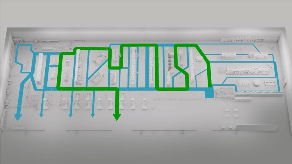 Figure 1: Analysis of Movement in a Retail Store, Showing Popular Routes
One of the primary markets for this technology is in the retail sector where large stores seek to understand better how customers move around the store so that they can maximize sales potential.
Beyond retail, asset tracking can also have a profound impact on industrial efficiency. It can be deployed to monitor material handling vehicles, reducing wasted time and improving efficiency. It can also be used to drive complex digital twins allowing for the accurate replication of movements in a virtual environment.
Asset tracking is not solely focused on improving efficiency; it also plays a significant role in ensuring safety. In warehouses and distribution centers, the use of tracking tags enables a safe coexistence of employees and industrial robotics, eliminating the possibility of collisions by allowing robots to track employee movements.
Basic System Design PrinciplesTo establish a position detection system, an array of antennas is placed in a building, whether that be a retail store, warehouse, hospital, airport, or other type of building. This array allows for highly accurate position measurement.
The methodology used can be either Angle of Arrival (AoA) or Angle of Departure (AoD). While both use the same radio frequency (RF) signal measurements, the signal processing and antenna configuration is different in each case.
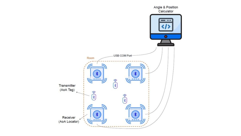 Figure 2: Anatomy of a Position Detection System
Typically, a system will consist of three main elements, a Bluetooth transmitter (AoA tag), a receiver/antenna array (AoA locator), and a system for calculating angle and position. To operate, the AoA tag sends a constant tone extension (CTE) signal.
This CTE signal spreads out in an expanding spherical pattern and is picked up by the antennas. As the wavelength/frequency of the signal is known, as is the distance between the receivers, then relatively simple trigonometry can be used to calculate the angle of the signal and, therefore, the transmitter based upon the phase difference of the signal arriving at each antenna.
Alternative Methods and Enhanced AccuracyBy performing the detection twice with two pairs of antennas, it is possible to triangulate the exact position of the AoA tag with a high degree of precision.
An alternative method that does not require angle measurement is trilateration. This is based upon a time-of-flight (ToF) distance measurement using Bluetooth 5.4 channel sounding (CS) feature or ultra-wideband (UWB).
CS is also known as high accuracy distance measurement (HADM) and many consider it to be a very accurate alternative to RSSI-based distance measurement.
onsemi’s RSL15 AoA SolutionThe RSL15 from onsemi is a Bluetooth 5.2 certified secure wireless microcontroller that is optimized for ultra-low power applications including industrial, medical and AoA. The device is based around an Arm Cortex-M33 processor running at up to 48 MHz and features encrypted security. Providing the industry’s lowest power consumption, the peak current when transmitting is just 4.3 mA and this reduces to 36 nA in sleep mode while waiting for a GPIO wakeup. It is designed to meet the demands of a wide range of tracking applications ranging from retail and clinical settings to manufacturing and distribution centers.
The post Position Tracking with Bluetooth Low Energy Technology appeared first on ELE Times.
Mission NIMpossible: Decoding the Microservices That Accelerate Generative AI
Sama Bali, Senior Product Marketer for AI solutions at NVIDIA Generative AI
Run generative AI NVIDIA NIM microservices locally on NVIDIA RTX AI workstations and NVIDIA GeForce RTX systems.
In the rapidly evolving world of artificial intelligence, generative AI is captivating imaginations and transforming industries. Behind the scenes, an unsung hero is making it all possible: microservices architecture.
The Building Blocks of Modern AI ApplicationsMicroservices have emerged as a powerful architecture, fundamentally changing how people design, build and deploy software.
A microservices architecture breaks down an application into a collection of loosely coupled, independently deployable services. Each service is responsible for a specific capability and communicates with other services through well-defined application programming interfaces, or APIs. This modular approach stands in stark contrast to traditional all-in-one architectures, in which all functionality is bundled into a single, tightly integrated application.
By decoupling services, teams can work on different components simultaneously, accelerating development processes and allowing updates to be rolled out independently without affecting the entire application. Developers can focus on building and improving specific services, leading to better code quality and faster problem resolution. Such specialization allows developers to become experts in their particular domain.
Services can be scaled independently based on demand, optimizing resource utilization and improving overall system performance. In addition, different services can use different technologies, allowing developers to choose the best tools for each specific task.
A Perfect Match: Microservices and Generative AIThe microservices architecture is particularly well-suited for developing generative AI applications due to its scalability, enhanced modularity and flexibility.
AI models, especially large language models, require significant computational resources. Microservices allow for efficient scaling of these resource-intensive components without affecting the entire system.
Generative AI applications often involve multiple steps, such as data preprocessing, model inference and post-processing. Microservices enable each step to be developed, optimized and scaled independently. Plus, as AI models and techniques evolve rapidly, a microservices architecture allows for easier integration of new models as well as the replacement of existing ones without disrupting the entire application.
NVIDIA NIM: Simplifying Generative AI DeploymentAs the demand for AI-powered applications grows, developers face challenges in efficiently deploying and managing AI models.
NVIDIA NIM inference microservices provide models as optimized containers to deploy in the cloud, data centers, workstations, desktops and laptops. Each NIM container includes the pretrained AI models and all the necessary runtime components, making it simple to integrate AI capabilities into applications.
NIM offers a game-changing approach for application developers looking to incorporate AI functionality by providing simplified integration, production-readiness and flexibility. Developers can focus on building their applications without worrying about the complexities of data preparation, model training or customization, as NIM inference microservices are optimized for performance, come with runtime optimizations and support industry-standard APIs.
AI at Your Fingertips: NVIDIA NIM on Workstations and PCsBuilding enterprise generative AI applications comes with many challenges. While cloud-hosted model APIs can help developers get started, issues related to data privacy, security, model response latency, accuracy, API costs and scaling often hinder the path to production.
Workstations with NIM provide developers with secure access to a broad range of models and performance-optimized inference microservices.
By avoiding the latency, cost and compliance concerns associated with cloud-hosted APIs as well as the complexities of model deployment, developers can focus on application development. This accelerates the delivery of production-ready generative AI applications — enabling seamless, automatic scale out with performance optimization in data centers and the cloud.
The recently announced general availability of the Meta Llama 3 8B model as a NIM, which can run locally on RTX systems, brings state-of-the-art language model capabilities to individual developers, enabling local testing and experimentation without the need for cloud resources. With NIM running locally, developers can create sophisticated retrieval-augmented generation (RAG) projects right on their workstations.
Local RAG refers to implementing RAG systems entirely on local hardware, without relying on cloud-based services or external APIs.
Developers can use the Llama 3 8B NIM on workstations with one or more NVIDIA RTX 6000 Ada Generation GPUs or on NVIDIA RTX systems to build end-to-end RAG systems entirely on local hardware. This setup allows developers to tap the full power of Llama 3 8B, ensuring high performance and low latency.
By running the entire RAG pipeline locally, developers can maintain complete control over their data, ensuring privacy and security. This approach is particularly helpful for developers building applications that require real-time responses and high accuracy, such as customer-support chatbots, personalized content-generation tools and interactive virtual assistants.
Hybrid RAG combines local and cloud-based resources to optimize performance and flexibility in AI applications. With NVIDIA AI Workbench, developers can get started with the hybrid-RAG Workbench Project — an example application that can be used to run vector databases and embedding models locally while performing inference using NIM in the cloud or data center, offering a flexible approach to resource allocation.
This hybrid setup allows developers to balance the computational load between local and cloud resources, optimizing performance and cost. For example, the vector database and embedding models can be hosted on local workstations to ensure fast data retrieval and processing, while the more computationally intensive inference tasks can be offloaded to powerful cloud-based NIM inference microservices. This flexibility enables developers to scale their applications seamlessly, accommodating varying workloads and ensuring consistent performance.
NVIDIA ACE NIM inference microservices bring digital humans, AI non-playable characters (NPCs) and interactive avatars for customer service to life with generative AI, running on RTX PCs and workstations.
ACE NIM inference microservices for speech — including Riva automatic speech recognition, text-to-speech and neural machine translation — allow accurate transcription, translation and realistic voices.
The NVIDIA Nemotron small language model is a NIM for intelligence that includes INT4 quantization for minimal memory usage and supports roleplay and RAG use cases.
And ACE NIM inference microservices for appearance include Audio2Face and Omniverse RTX for lifelike animation with ultrarealistic visuals. These provide more immersive and engaging gaming characters, as well as more satisfying experiences for users interacting with virtual customer-service agents.
Dive Into NIMAs AI progresses, the ability to rapidly deploy and scale its capabilities will become increasingly crucial.
NVIDIA NIM microservices provide the foundation for this new era of AI application development, enabling breakthrough innovations. Whether building the next generation of AI-powered games, developing advanced natural language processing applications or creating intelligent automation systems, users can access these powerful development tools at their fingertips.
The post Mission NIMpossible: Decoding the Microservices That Accelerate Generative AI appeared first on ELE Times.
Futureproof Your Industrial Network Security
Courtesy: Moxa
Today, industrial organizations are embracing digital transformation to gain a competitive edge and boost business revenue. To achieve digital transformation, industrial operators must first address the daunting task of merging their information technology (IT) and operational technology (OT) infrastructure. However, businesses trying to streamline data connectivity for integrated IT/OT systems often encounter challenges such as lacking performance, limited network visibility, and lower network security from existing OT network infrastructure. Building a robust, high-performance network for daily operations that is easy to maintain requires thorough planning. In this article, we will focus on the importance of strong OT network security and provide some tips on how to strengthen cybersecurity for industrial operations.
Why Ramping Up OT Network Security Is a MustNowadays, industrial applications are facing more and unprecedented cyberthreats. These threats often target critical infrastructure in different industries all across the world, including energy, transportation, and water and wastewater services. If successful, such attacks can cause significant damage to industrial organizations in the form of high recovery costs or production delays. Before building IT/OT converged networks, asset owners must define the target security level of the entire network and strengthen measures to minimize the impact of potential intrusions. Poor network security exposes critical field assets to unwanted access and allows malicious actors to breach integrated systems.
However, strengthening OT network security is not that straightforward. IT security solutions require constant updates to ensure they can protect against the latest cyberthreats. Applying these necessary updates often means interrupting network services and systems, which is something OT operations cannot afford. Operators need an OT-centric cybersecurity approach to protect their industrial networks without sacrificing network or operational uptime.
Three Major Stages of Building OT CybersecurityBuilding a secure industrial network can be done with the right approach. The key to strong cybersecurity is implementing a multi-layered defense strategy in several stages.
Stage One: Build a Solid Foundation with Secure Networking DevicesWhen developing secure networking infrastructure, start with choosing secure building blocks. The increasing number of cyberthreats has also led to the development of comprehensive OT network security standards. Industrial cybersecurity standards, such as NIST CSF and IEC 62443, provide security guidelines for critical assets, systems, and components. Implementing industrial cybersecurity standards and using networking devices designed around these standards provides asset owners with a solid foundation for building secure network infrastructure.
Stage Two: Deploy OT-centric Layered ProtectionThe idea of defense-in-depth is to provide multi-layered protection by implementing cybersecurity measures at every level to minimize security risks. In the event of an intrusion, if one layer of protection is compromised, another layer prevents the threat from further affecting the network. In addition, instant notifications for security events allow users to quickly respond to potential threats and mitigate any risk.
When deploying multi-layered network protection for OT networks and infrastructure, there are two key OT cybersecurity solutions to consider, namely industrial firewalls and secure routers.
Shield Critical Assets with Industrial FirewallsAn efficient way to protect critical field assets is using industrial firewalls to create secure network zones and defend against potential threats across the network. With every connected device being the potential target of cyberthreats, it’s important to deploy firewalls with robust traffic filtering that allow administrators to set up secure conduits throughout the network. Next-generation firewalls feature advanced security functions such as Intrusion Detection/Prevention Systems (IDS/IPS) and Deep Packet Inspection (DPI) to strengthen network protection against intrusions by proactively detecting and blocking threats.
Advanced security functions tailored for OT environments help ensure seamless communications and maximum uptime for industrial operations. For example, OT-centered DPI technology that supports industrial protocols can detect and block unwanted traffic, ensuring secure industrial protocol communications. In addition, industrial-grade IPS can support virtual patching to protect critical assets and legacy devices from the latest known threats without affecting network uptime. Designed for industrial applications, IPS provides pattern-based detection for PLCs, HMIs, and other common field site equipment.
Fortify Network Boundaries with Industrial Secure RoutersIT/OT converged networks require a multi-layered and complex industrial network infrastructure to transmit large amounts of data from field sites to the control center. Deploying powerful industrial secure routers between different networks can both fortify network boundaries and maintain solid network performance. Featuring built-in advanced security functions such as firewall and NAT, secure routers allow administrators to establish secure network segments and enable data routing between segments. For optimal network performance, a powerful industrial secure router features both switching and routing functions with Gigabit speeds, alongside redundancy measures for smooth intra- and inter-network communication.
The demand for remote access to maintain critical assets and networks has also been on the rise. Industrial secure routers with VPN support allow maintenance engineers and network administrators to access private networks remotely through a secure tunnel, enabling more efficient remote management.
Stage Three: Monitor the Network Status and Identify CyberthreatsDeploying a secure industrial network is just the start of the journey towards robust cybersecurity. During daily operations, it takes a lot of time and effort for network administrators to have full network visibility, monitor traffic, and manage the countless networking devices. Implementing a centralized network management platform can provide a huge boost to operational efficiency by visualizing the entire network and simplifying device management. It also allows network administrators to focus more resources on ramping up network and device security.
In addition, a centralized network security management platform for cybersecurity solutions can boost efficiency even more. Such software allows administrators to perform mass deployments for firewall policies, monitor cyberthreats, and configure notifications for when threats occur. The right combination of cybersecurity solutions and management software offers administrators an invaluable way to monitor and identify cyberthreats with a holistic view.
Futureproof Network Security with Our SolutionsNetwork security is imperative for industrial network infrastructure. Moxa has translated over 35 years of industrial networking experience into a comprehensive OT-centric cybersecurity portfolio that offers enhanced security with maximum network uptime. Moxa is an IEC 62443-4-1 certified industrial connectivity and networking solutions provider. When developing our products, we adhere to the security principles of the IEC 62443-4-2 standard to ensure secure product development. Our goal is to provide our users with the tools necessary to build robust device security for their industrial applications.
To defend against increasing cyberthreats, our OT-focused cybersecurity solutions maximize uptime while protecting industrial networks from intruders. Our network management software simplifies management for networking devices and OT cybersecurity solutions, allowing administrators to monitor the network security status and manage cyberthreats with ease.
The post Futureproof Your Industrial Network Security appeared first on ELE Times.
Why the performance of your storage system matters for AI workloads?
Courtesy: Micron
A guide to understanding some key factors that influence the speed and efficiency of your data storage
Data is the lifeblood of any modern business, and how you store, access and manage it can make a dramatic difference in your productivity, profitability and competitiveness. The emergence of artificial intelligence (AI) is transforming every industry and forcing businesses to re-evaluate how they can use data to accelerate innovation and growth. However, AI training and inferencing pose unique challenges for data management and storage, as they require massive amounts of data, high performance, scalability and availability.
Not all storage systems are created equal, and many factors that can affect their performance. In this blog post, we will explore some of the main factors that influence storage system performance for AI and, importantly, how your choice of underlying storage media will affect them.
Key attributes of AI workloadsAI workloads are data-intensive and compute-intensive, meaning that they need to process large volumes of data at high speed and with low latency. Storage plays a vital role in enabling AI workloads to access, ingest, process and store data efficiently and effectively. Some key attributes of typical AI workloads that affect storage requirements are:
- Data variety: AI workloads need to access data from multiple sources and formats, such as structured, unstructured or semi-structured data, and from various locations, such as on-premises, cloud or edge. Storage solutions need to provide fast and reliable data access and movement across different environments and platforms.
- Data velocity: AI workloads need to process data in real-time or near-real-time. Storage solutions need to deliver high throughput, low latency and consistent performance for data ingestion, processing and analysis.
- Data volume: As AI models grow in complexity and accuracy and GPU clusters grow in compute power, their storage solutions need to provide flexible and scalable capacity and performance.
- Data reliability and availability: AI workloads need to ensure data integrity, security and extremely high availability, particularly when connected to large GPU clusters that are intolerant of interruptions in data access.
Storage system performance is not a single metric but a combination of several factors that depend on the characteristics and requirements of your data, applications and data center infrastructure. Some of the most crucial factors are:
- Throughput: The rate at which your storage system can transfer data to and from the network or the host. Higher throughput can improve performance by increasing the bandwidth and reducing the congestion and bottlenecks of your data flow. The throughput is usually limited by either the network bandwidth or the speed of the storage media.
- Latency: The time it takes for your storage system to respond to a read or write request. A lower latency can improve performance by reducing GPU idle time and improving the system’s responsiveness to user inputs. The latency of mechanical devices (such as HDDs) is inherently much higher than for solid-state devices (SSDs).
- Scalability: The ability of your storage system to adapt to changes in data volume, velocity and variety. High scalability is key to enabling your storage system to grow and evolve with your business needs and goals. The biggest challenge to increasing the amount of data that your system can store and manage is maintaining performance scaling without hitting bottlenecks or storage device limitations.
- Resiliency: The ability of your storage system to maintain data integrity and availability in the event of failures, errors or disasters. Higher reliability can improve performance by reducing the frequency and impact of data corruption, loss and recovery.
Hard disk drives (HDDs) and solid-state drives (SSDs) are the two main types of devices employed for persistent storage in data center applications. HDDs are mechanical devices that use rotating disk platters with a magnetic coating to store data, while SSDs use solid-state flash memory chips to store data. HDDs have been the dominant storage devices for decades. HDDs offer the lowest cost per bit and long-term, power-off durability, but they are slower and less reliable than SSDs. SSDs offer higher throughputs, lower latencies, higher reliability and denser packaging options.
As technology advances and computing demands increase, the mechanical nature of the HDD may not allow it to keep pace in performance. There are a few options that system designs can deploy to extend the effective performance of HDD-based storage systems, such as mixing hot and cold data (hot data borrowing performance from the colder data), sharing data across many HDD spindles in parallel (increasing throughput but not improving latency), overprovisioning HDD capacity (in essence provisioning for IO and not capacity), and adding SSD caching layers for latency outliers (see recent blog by Steve Wells HDDs and SSDs. What are the right questions? | Micron Technology Inc.). These system-level solutions have limited scalability before their cost becomes prohibitive. How extendable these solutions are is dependent on the level of performance an application requires. For many of today’s AI workloads, HDD-based systems are falling short on scalability of performance and power efficiency.
High-capacity, SSD-based storage systems, though, can provide a less complex and more extendable solution, and they are rapidly evolving as the storage media of choice for high-performance AI data lakes at many large GPU-centric data centers. While at the drive level, on a cost-per-bit basis, these SSDs are more expensive than HDDs. But at a system level, systems built with these SSDs can have better operating costs than HDDs when you consider these improvements:
- Much higher throughput
- Greater than 100 times lower latency
- Fewer servers and racks per petabyte needed
- Better reliability with longer useful lifetimes
- Better energy efficiency for a given level of performance
The capacity of SSDs is expected to grow to over 120TB in the next few years. As their capacities grow and the pricing gap between SSDs and HDDs narrows, these SSDs can become attractive alternatives for other workloads that demand higher than average performance or need much lower latency on large data sets, such as video editing and medical imaging diagnostics.
ConclusionStorage performance is an important design criterion for systems running AI workloads. It affects system performance, scalability, data availability and overall system cost and power requirements. Therefore, it’s important that you understand the features and benefits of different storage options and select the best storage solution for your AI needs. By choosing the right storage solution, you can optimize your AI workloads and achieve your AI goals.
The post Why the performance of your storage system matters for AI workloads? appeared first on ELE Times.
Semiconductor Attributes for Sustainable System Design
Courtesy: Jay Nagle, Principal Product Marketing Engineer, Microchip Technology Inc.
Jay Nagle, Principal Product Marketing Engineer, Microchip Technology Inc.
Gain further insights on some of the key attributes required of semiconductors to facilitate sustainability in electronic systems design.
Semiconductor Innovations for Sustainable Energy ManagementAs systems design becomes more technologically advanced, the resultant volume increase in electronic content poses threats to environmental sustainability. Global sustainability initiatives are being implemented to mitigate these threats. However, with the rise of these initiatives, there is also an increasing demand for the generation of electricity. Thus, a new challenge emerges: how can we manage these increasing levels of energy consumption?
To answer the call for more electricity generation, it is essential for renewable energy sources to have increasing shares of energy production vs. fossil fuels to reduce greenhouse gas emissions. The efficiency of a renewable energy source hinges on optimizing the transfer of energy from the source to the power grid or various electrical loads. These loads include commonly utilized consumer electronics, residential appliances and large-scale battery energy storage systems. Furthermore, the electrical loads must utilize an optimal amount of power during operation to encourage efficient energy usage.
Read on to learn more about the key attributes of semiconductors that contribute to enhanced sustainability in system designs.
Integrated circuits (ICs) or application-specific integrated circuits (ASICs) used for renewable power conversion and embedded systems must have four key features: low power dissipation, high reliability, high power density and security.
Low Power DissipationOne of the main characteristics needed in a semiconductor for sustainable design is low power consumption. This extends battery life, allowing longer operating times between recharges, which ultimately conserves energy.
There are two leading sources of semiconductor power loss. The first is static power dissipation or power consumption when a circuit is in stand-by or a non-operational state. The second source is dynamic power dissipation, or power consumption when the circuit is in an operational state.
To reduce both static and dynamic power dissipation, semiconductors are developed to minimize capacitance through their internal layout construction, operate at lower voltage levels and activate functional blocks depending on if the device is in “deep sleep” stand-by or functional mode.
Microchip offers low power solutions that are energy efficient and reduce hazardous e-waste production.
High ReliabilityThe reliability of parts and the longevity of the system help to measure performance of semiconductors in sustainable system designs. Semiconductor reliability and longevity can be compromised by operation near the limits of the device’s temperature ratings, mechanical stresses, and torsion.
We use Very Thin Quad Flat No-Lead (VQFN) and Thin Quad Flat Pack (TQFP) packages to encapsulate complex layouts in small form factor packages to address these concerns. Exposed pads on the bottom surface of the VQFN package dissipate an adequate amount of heat, which helps to hold a low junction to case thermal resistance when the device operates at maximum capacity. TQFP packages use gull-wing leads on low-profile height packages to withstand torsion and other mechanical stresses.
High Power DensityPower density refers to the amount of power generated per unit of die size. Semiconductors with high power densities can run at high power levels while being packaged in small footprints. This is common in silicon carbide (SiC) wide-bandgap (WBG) discretes and power modules used in solar, wind and electric-vehicle power-conversion applications.
SiC enhances power-conversion systems by allowing the system to operate at higher frequencies, reducing the size and weight of electrical passives needed to transfer the maximum amount of power from a renewable source.
Our WBG SiC semiconductors offer several advantages over traditional silicon devices, such as running at higher temperatures and faster switching speeds. SiC devices’ low switching losses improve system efficiency while their high-power density reduces size and weight. They also can achieve a smaller footprint with reduction in heat sink dimensions.
SecuritySecurity in semiconductors is almost synonymous with longevity, as security features can enable continued reuse of existing systems. This means that the design can be operated for longer periods of time without the need for replacement or becoming outdated.
There are helpful security features that support system longevity. For example, secure and immutable boot can verify the integrity of any necessary software updates to enhance system performance or fix software bugs. Secure key storage and node authentication can protect against external attacks as well as ensure that verified code runs on the embedded design.
The post Semiconductor Attributes for Sustainable System Design appeared first on ELE Times.
Pulsus Is a Breakthrough for PiezoMEMS Devices
Courtesy: Lam Research
- The tool enables the deposition of high-quality, highly scandium-doped AlScN films
- Features include dual-chamber configuration, degas, preclean, target library, precise laser scanning, and more
In this post, we explain how the Pulsus system works, and how it can achieve superior film quality and performance compared to conventional technologies.
PiezoMEMS devices are microelectromechanical systems that use piezoelectric materials to convert electrical energy into mechanical motion, or vice versa. They have applications in a wide range of fields, including sensors, actuators, microphones, speakers, filters, switches, and energy harvesters.
PiezoMEMS devices require high-quality thin films of piezoelectric materials, such as aluminum scandium nitride (AlScN), to achieve optimal performance. Conventional deposition technologies—think sputtering or chemical vapor deposition—face challenges in producing AlScN films with desired properties, such as composition, thickness, stress, and uniformity. These obstacles limit both the scalability and functionality of piezoMEMS devices.
Revolutionary TechTo help overcome these challenges, Lam Research recently introduced Pulsus, a pulsed laser deposition (PLD) system that we hope will revolutionize the world of piezoMEMS applications. The addition of Pulsus PLD to the Lam portfolio further expands our comprehensive range of deposition, etch and single wafer clean products focused on specialty technologies and demonstrates Lam’s continuous innovation in this sector.
Pulsus is a PLD process module that has been optimized and integrated on Lam’s production-proven 2300 platform. It was developed to enable the deposition of high-quality AlScN films, which are essential to produce piezoMEMS devices.
A key benefit of the Pulsus system is its ability to deposit multi-element thin films, like highly scandium-doped AlScN. The intrinsic high plasma density—in combination with pulsed growth—creates the conditions to stabilize the elements in the same ratio as they arrive from the target. This control is essential for depositing materials where the functionality of the film is driven by the precise composition of the elements.
Plasma, LasersLocal plasma allows for high local control of film specifications across the wafer, like thickness and local in-film stress. Pulsus can adjust deposition settings while the plasma “hovers” over the wafer surface. This local tuning of thickness and stress allows for high uniformities over the wafer, which is exactly what our customers are asking for. And because the plasma is generated locally, Pulsus uses targets that are much smaller than you would typically see in PVD systems. Pulsus can exchange these smaller targets, without breaking vacuum, through a target exchange module—the target library.
Pulsus uses a pulsed high-power laser to ablate a target material, in this case AlScN, and create a plasma plume. The plume expands and impinges on a substrate, where it forms a thin film.
Pulsus has a fast and precise laser optical path which, in combination with the target scanning mechanism, allows for uniform and controlled ablation of the target material. The Pulsus system has a high control of plasma plume generation, wafer temperature, and pressure control to achieve the desired film composition and stoichiometry.
By combining these features, Pulsus can produce high-quality films with superior performance for piezoMEMS devices. Pulsus can achieve excellent composition control, with low variation of the scandium (Sc) content across the wafer and within individual devices. It also delivers high film uniformity, with low WiW (within-wafer) and wafer-to-wafer (WtW) variation of the film thickness and stress.
Breakthrough TechnologyPulsus is a breakthrough technology for AlScN deposition, which can improve film quality and performance for piezoMEMS applications. In addition, Pulsus has the potential to enhance the functionality and scalability of piezoMEMS devices. The Pulsus technology deposits AlScN films with very high Sc concentration, resulting in high piezoelectric coefficients, which drive higher device sensitivity and output. These films feature tunable stress states to enable the design of different device configurations and shapes.
Pulsus is currently in use on 200 mm wafers and is planned to expand to 300 mm wafers in the future—a move that has the potential to increase the productivity and yield of piezoMEMS devices.
The post Pulsus Is a Breakthrough for PiezoMEMS Devices appeared first on ELE Times.
4K and beyond: Trends that are shaping India’s home projector market
Sushil Motwani, founder of Aytexcel Pvt Ltd, also evaluates the change in customer preferences that is driving the growth of the home entertainment segment
 Sushil Motwani, Founder of Aytexcel Pvt. Ltd. and Official India Representative of Formovie
Recent news reports indicate that a few leading companies in the home entertainment industry are in discussions with major production studios to ensure 8K resolution content, which offers extremely high-definition video quality. This means that the availability of 8K content is on the verge of becoming normative. From the modern consumer looking for the best visual experience, this is an exciting prospect.
Even though the availability of 8K content is currently minimal, many projectors boosted by technologies like Artificial Intelligence (AI) can upscale 4K content. While this cannot match the true quality of the native 8K, improved versions are expected in the coming years.
In the case of 4K and beyond, devices like laser projectors are continually evolving to match user preferences. Until the COVID-19 pandemic, laser projectors were mainly used for business presentations, in the education sector and at screening centres. However, with the rise of more OTT platforms and the availability of 4K content, there has been a huge demand for home theatres, where projector screens have replaced traditional TVs.
According to Statista, the number of households in India using home entertainment systems, such as home theatres, projectors and advanced TVs, is expected to reach 26.2 million by 2028. The revenue in this segment is projected to show an annual growth rate (CAGR) of 3.70 per cent, resulting in an estimated market volume of US$0.7 billion by 2028.
So, what are the key trends driving the home projector market in India? Visual quality is definitely one of them. Modern consumers demand upgraded display technologies like the Advanced Laser Phosphor Display® (ALPD). This innovative display combines laser-excited fluorescent materials with multi-colour lasers, resulting in a smooth and vividly coloured display, superior to regular projectors.
Multifunctionality is another key requirement for gamers. When transitioning from PCs to projector-driven gaming, consumers look for a large screen size, preferably 120 inches and above, high resolution, low input lag, quick refresh rate and excellent detailing and contrast.
With the integration of AI and Machine Learning (ML) tools, manufacturers are developing projectors with more user-friendly features and automatic settings that adjust to surrounding light conditions based on the displayed content. AI also helps improve security features and facilitates personalised user modes, while predictive maintenance makes the devices more intuitive and efficient.
Projectors with a multifaceted interface are also a popular choice. Voice assistance features enable users to connect their large-screen setups with other smart devices. The user experience is enhanced by options such as Alexa or voice commands through Google Assistant using a Google Home device or an Android smartphone. Multiple connectivity options, including HDMI, USB, Bluetooth and Wi-Fi facilitate smooth handling of these devices. Consumers also prefer projectors with native app integrations, like Netflix, to avoid external setups while streaming content.
There is also a desire among users to avoid messy cables and additional devices, which not only affect the convenience of installation but also impact the aesthetics of the interiors. This is why Ultra Short Throw (UST) projectors, which can offer a big screen experience even in small spaces, are emerging as a top choice. Some of these projectors can throw a 100-inch projection with an ultra-short throw distance of just 9 inches from the wall.
And finally, nothing can deliver a true cinematic experience like a dedicated surround sound system. But customers also want to avoid the additional setup of soundbars and subwoofers for enhanced sound. Since most movies are now supported by Dolby Atmos 7.1 sound, the home theatre segment is also looking for similar sound support. Projectors integrated with Dolby Atmos sound, powered by speakers from legendary manufacturers like Bowers & Wilkins, Yamaha, or Wharfedale, are key attractions for movie lovers and gamers.
Buyers are also looking for eye-friendly projectors equipped with features like infrared body sensors and diffuse reflection. The intelligent light-dimming and eye care technologies make their viewing experience more comfortable and reduce eye strain, especially during prolonged sessions like gaming.
The growing popularity of projectors is also attributed to the increasing focus on sustainability. Laser projectors are more energy-efficient than traditional lamp-based projectors. They use almost 50 per cent less power compared to the latter, which helps in energy savings and reduces the overall environmental impact. They are also very compact and made with sustainable and recycled materials, which minimises the logistical environmental impact and carbon footprint associated with their operation.
The post 4K and beyond: Trends that are shaping India’s home projector market appeared first on ELE Times.
An Overview of Oscilloscopes and Their Industrial Uses
Key takeaways:
- Oscilloscopes are primarily time-domain measurement instruments that mostly display timing-related characteristics.
- However, mixed-domain oscilloscopes give you the best of both worlds by including built-in spectrum analyzers for frequency-domain measurements.
- Modern oscilloscopes sport extremely sophisticated triggering and analysis features, both on-device and through remote measurement software.
After a multimeter, an oscilloscope is probably the second-most popular instrument on an engineer’s workbench. Oscilloscopes enable you to peer into the internals of electronic devices and monitor the signals they use under the hood.
What do engineers look for when using oscilloscopes? What are some innovations that these instruments have facilitated? What are some key characteristics to look for? Find out the answers to all this and more below.
What is the primary function of oscilloscopes in electronic measurements?Oscilloscopes enable engineers to measure and visualize the amplitude of an electrical signal over time. This is also the reason they are generally considered time-domain measurement instruments. However, there are mixed-domain oscilloscopes that provide both time-domain (amplitude vs. time) and frequency-domain (power vs. frequency) measurements.
The precise characterization of waveforms is a critical diagnostic tool in every stage of an electronic product lifecycle, including cutting-edge research, prototyping, design, quality assurance, compliance, maintenance, and calibration.
Let’s look at the type of signals that are being tested with oscilloscopes in various industries to facilitate innovations and products.
What signal characteristics are verified using oscilloscopes?When experienced electronics engineers are troubleshooting issues using oscilloscopes, they are looking for evidence of several ideal characteristics as well as problematic phenomena, depending on the type of signal and the application. Some of the common aspects and phenomena they examine are listed below:
- Signal shape: The waveform should match the expected shape if the specification requires a square, sawtooth, or sine wave. Any deviations might indicate an issue.
- Amplitude: The signal levels should remain within the expected range of volts without excessive fluctuations.
- Frequency or period: The frequency or period of the signal should always remain within specified limits. Deviations from the expected frequency can lead to synchronization problems in communication and control systems.
- Rise and fall times: For digital signals, sharp and consistent rise and fall times are essential for reliable operation. If the rise time is slower than required, it may lead to problems like data corruption, timing errors, and reduced performance in digital circuits. If it’s overly fast, it can lead to increased electromagnetic interference as well as signal integrity issues like ringing and crosstalk.
- Jitter: Jitter is the variation in a signal characteristic during significant transitions. Period jitter is the variation in the duration of individual clock periods. Cycle-to-cycle jitter is the variation in duration between consecutive clock cycles. Phase jitter is the variation in the phase of the signal with respect to a reference clock. Timing jitter is the variation in the timing of signal edges. Low jitter indicates stable signal timing. Excessive jitter may cause errors in high-speed digital communication.
- Phase consistency: In systems with multiple signals, phase consistency between them is critical for proper synchronization.
- Duty cycle: For pulse-width modulation signals and clock signals, the duty cycle should be as specified.
- Noise: Noise is any unwanted disturbance that affects a signal’s amplitude, phase, frequency, or other characteristics. It should be minimal and within acceptable limits to avoid interference and degradation of the signal. Too much noise indicates poor signal integrity, possible shielding issues, or noise due to suboptimal power supply. Phase noise can affect the synchronization of communication and clock signals.
- Harmonics and distortion: For analog signals, low harmonic distortion ensures signal fidelity.
- Ringing: Ringing refers to oscillations after a signal transition, usually seen in digital circuits, that can lead to errors and signal integrity issues.
- Crosstalk: Unwanted coupling from adjacent signal lines can appear as unexpected waveforms on the oscilloscope trace.
- Drift: Changes in signal amplitude or frequency over time are indicators of instability in the power supply or other components.
- Ground bounce: Variability in the ground potential, often visible as a noisy baseline, can be critical in fast-switching digital circuits.
- Clipping: If the input signal amplitude exceeds the oscilloscope’s input range, the displayed waveform will be clipped, indicating a need for signal attenuation or a more appropriate input setting on the scope.
- Direct current (DC) offsets: Unexpected DC offsets can indicate issues with the waveform generation or coupling methods.
- Aliasing: Aliasing occurs if the oscilloscope sampling rate is too low for the signal frequency, leading to an incorrect representation of the signal.
Oscilloscopes are used to verify a variety of analog signals and digital signals in many industries as explained below.
5G and 6G telecom
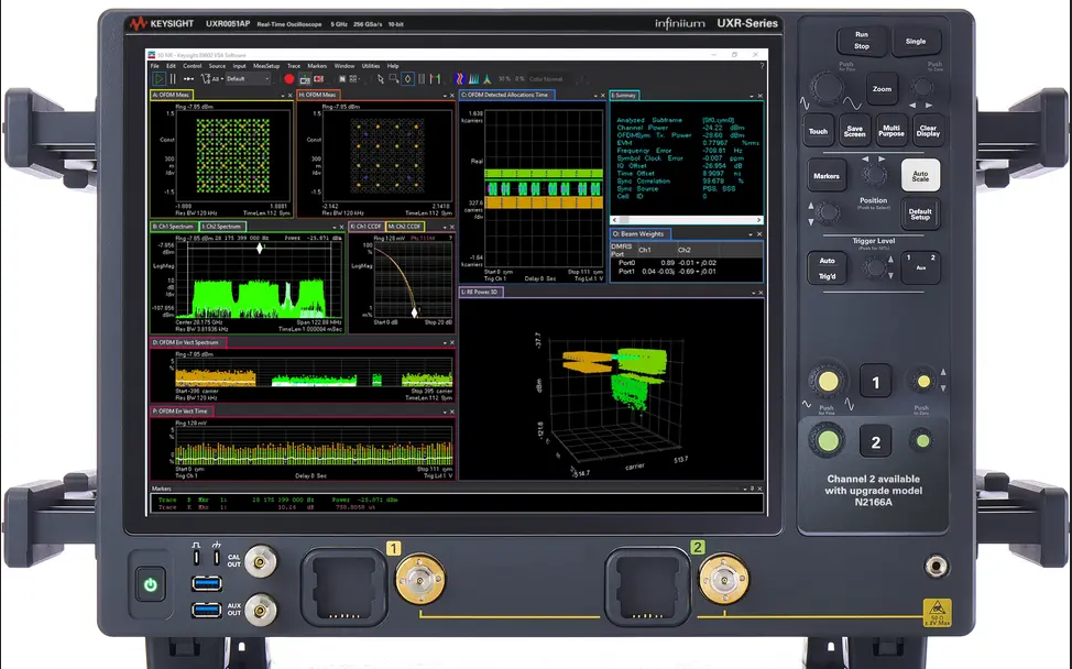 Figure 1: A Keysight Infiniium UXR-series real-time oscilloscope
The radio frequency (RF) signals used in telecom systems and devices must strictly adhere to specifications for optimum performance as well as regulatory compliance.
Some examples of oscilloscope use in this domain include:
- InfiniiumUXR-B series real-time oscilloscopes (RTOs) for characterizing 5G and 6G systems, including phased-array antenna transceivers and mmWave wideband analysis capable of measuring frequencies as high as 110 gigahertz (GHz) and bandwidths of as much as 5 GHz
- development and verification of 41-GHz power amplifier chips for 5G New Radio applications
- qualifying a 6G 100 gigabits-per-second (Gbps) 300GHz (sub-terahertz) wireless data link using a 70 GHz UXR0704B Infiniium UXR-Series RTO
Oscilloscopes are extensively employed for functional and compliance testing of optical and electrical transceivers used in high-speed data center networks.
Some of the use cases are listed below:
- Oscilloscopes, with the help of optical-to-electrical adaptors, verify characteristics like phase-amplitude modulation (PAM4) of 400Ghigh-speed optical networks.
- Oscilloscopes test the conformance of 400G/800G electrical data center transceivers with the Institute of Electrical and Electronics Engineers (IEEE) 802.3CK and the Optical Internetworking Forum’s (OIF) OIF-CEI-5.0 specifications.
- Real-time oscilloscopes like the UXR-B are used to evaluate the forward error correction performance of high-speed optical network links.
Oscilloscopes and arbitrary waveform generators are used together for debugging and automated testing of high-speed digital interfaces like:
- Wi-Fi 7 networking standard
- universal serial bus (USB)
- mobile industry processor interface (MIPI) standards
- peripheral component interconnect express (PCIe) buses
- high-definition multimedia interface (HDMI)
They are also being used for testing general-purpose digital interfaces like the inter-integrated circuit (I2C), the serial peripheral interface (SPI), and more.
Automotive radars and in-vehicle networks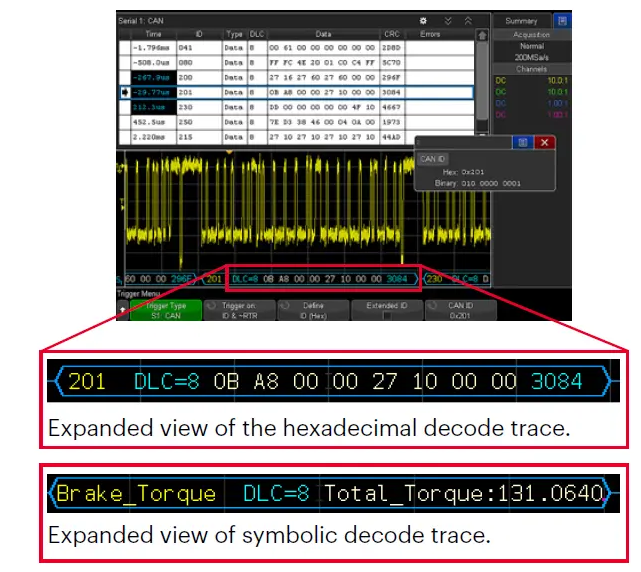 Figure 2: Integrated protocol decoders for automotive and other digital signals
Oscilloscopes are used for validating automotive mmWave radar chips. Additionally, oscilloscopes are extensively used for verifying automotive in-vehicle network signals like:
- automotive Ethernet
- controller area network (CAN)
- FlexRay
- local interconnect network (LIN)
Radars for aerospace and defense uses are validated using instruments like the UXR-series oscilloscopes.
They are also used for ensuring that data communications comply with standards like the MIL-STD 1553 and ARINC 429.
SpaceOscilloscopes are being used for developing 2.65 Gbps high-speed data links to satellites.
How does an oscilloscope visually represent electrical signals?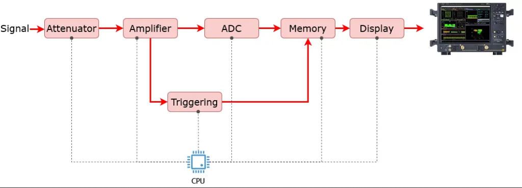 Figure 3: Schematic of an oscilloscope
An oscilloscope’s display panel consists of a two-dimensional resizable digital grid. The horizontal X-axis represents the time base for the signal, while the vertical Y-axis represents signal amplitude in volts.
Each segment of an axis is called a division (or div). Control knobs on the oscilloscope allow the user to change the magnitude of volts or time that each div represents.
 Figure 4: Visualizing a signal on an oscilloscope
Increasing this magnitude on the X-axis means more seconds or milliseconds per division. So you can view a longer capture of the signal, effectively zooming out on it. Similarly, by reducing the magnitude on the X-axis, you’re able to zoom into the signal to see finer details. The maximum zoom depends on the oscilloscope’s sampling rate. It’s often possible to zoom in to nanosecond levels on modern oscilloscopes since they have sampling rates of some giga samples per second.
Similarly, you can zoom in or out on the Y-axis to examine finer details of changes in amplitude.
What are the various types of oscilloscopes?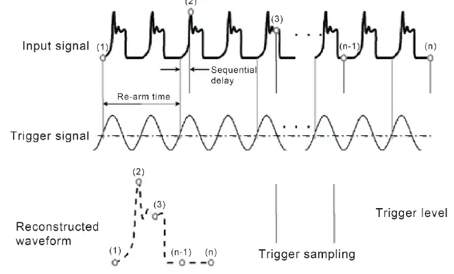 Figure 5:Waveform acquisition using an equivalent time sampling oscilloscope
Some of the common types of oscilloscopes are:
- Digital storage oscilloscopes (DSOs): They capture and store digital representations of analog signals, allowing for detailed analysis and post-processing. All modern scopes, including the sub-types below, are DSOs. The term differentiates them from older analog scopes that showed waveforms by firing an electron beam from a cathode ray tube (CRT) onto a phosphor-coated screen to make it glow.
- Mixed-signal oscilloscopes (MSOs): They integrate both analog and digital channels, enabling simultaneous observation of analog signals and digital logic states. They’re useful for use cases like monitoring power management chips.
- Mixed-domain oscilloscopes (MDOs): They combine normal time-domain oscilloscope functions with a built-in spectrum analyzer, allowing for time-correlated viewing of time-domain and frequency-domain signals.
- Real-time oscilloscopes: They capture and process a waveform in real time as it happens, making them suitable for non-repetitive and transient signal analysis.
- Equivalent time oscilloscopes: Equivalent time or sampling oscilloscopes are designed to capture high-frequency or fast repetitive signals by reconstructing them using equivalent time sampling. They sample a repetitive input signal at a slightly different point of time during each repetition. By piecing these samples together, they can reconstruct an accurate representation of the waveform, even one that is very high frequency.
Oscilloscopes often complement other instruments like spectrum analyzers and logic analyzers. Some key differences between oscilloscopes and spectrum analyzers include:
- Purpose: Oscilloscopes show how a signal changes over time by measuring its amplitude. Spectrum analyzers show how the energy of a signal is spread over different frequencies by measuring the power at each frequency.
- Displayed information: Oscilloscopes show time-related information like rise and fall times, phase shifts, and jitter. Spectrum analyzers show frequency-related information like signal bandwidth, carrier frequency, and harmonics.
- Uses: Oscilloscopes are extensively used for visualizing signals in real time and near real time. Spectrum analyzers are useful when frequency analysis is critical, such as in radio frequency communications and electromagnetic interference testing.
A mixed-domain oscilloscope combines oscilloscope and spectrum analyzer capabilities in a single instrument with features like fast Fourier transforms (FFT) to convert between the two domains.
Another complementary instrument is a logic analyzer. Both mixed-signal oscilloscopes and logic analyzers are capable of measuring digital signals. But they differ in some important aspects:
- Analog and digital signals: An MSO can measure both analog and digital signals. However, logic analyzers only measure digital signals.
- Number of channels: Most oscilloscopes support two to four channels and a few top out around eight. In sharp contrast, logic analyzers can support dozens to hundreds of digital signals.
- Analysis capabilities: Oscilloscopes provide sophisticated triggering options for capturing complex analog signals. But logic analyzers can keep it relatively simple since they only focus on digital signals.
 Figure 6: A Keysight UXR-B series scope
The most important specifications and features to consider when choosing an oscilloscope include:
- Bandwidth: For analog signals, the recommended bandwidth is three times or more of the highest sine wave frequency. For digital signals, the ideal bandwidth is five times or more of the highest digital clock rate, measured in hertz (Hz), megahertz (MHz), or GHz.
- Sample rate: This is the number of times the oscilloscope measures the signal each second. State-of-the-art oscilloscopes, like the UXR series, support up to 256 giga samples (billion samples) per second, which works out to a measurement taken every four femtoseconds. The sample rate dramatically impacts the signal you see on the display. An incorrect sample rate can result in an inaccurate or distorted representation of a signal. A low sample rate can cause errors to go undetected because they can occur between collected samples. The sample rate should be at least twice the highest frequency of the signal to avoid aliasing, but a sample rate of 4-5 times the bandwidth is often recommended to precisely capture signal details.
- Waveform update rate: A higher waveform rate increases the chances of detecting possible glitches and other infrequent events that occur during the blind time between two acquisitions.
- Number of channels: Most use cases are mixed-signal environments with multiple analog and digital signals. Select an oscilloscope with sufficient channels for critical time-correlated measurements across multiple waveforms.
- Effective number of bits (ENOB): ENOB says how many bits are truly useful for accurate measurements. Unlike the total analog-to-digital converter (ADC) bits, which can include some bits influenced by noise and errors, ENOB reflects the realistic performance and quality of the oscilloscope’s measurements.
- Signal-to-noise ratio (SNR): This is the ratio of actual signal information to noise in a measurement. Low SNR is recommended for higher accuracy.
- Time base accuracy: This tells you the timing accuracy in parts per billion.
- Memory depth: This is specified as the number of data points that the scope can store in memory. It determines the longest waveforms that can be captured while measuring at the maximum sample rate.
Some emerging trends in oscilloscopes and onboard embedded software are in the areas of signal analysis, automated compliance testing, and protocol decoding capabilities:
Advances in signal analysis include:
- deep signal integrity analysis for high-speed digital applications
- advanced statistical analysis of jitter and noise in digital interfaces in the voltage and time domains
- analysis of high-speed PAM data signals
- power integrity analysis to understand the effects of alternating or digital signals and DC supplies on each other
- de-embedding of cables, probes, fixtures, and S-parameters to remove their impacts from measurements for higher accuracy
Automated compliance testing software can automatically check high-speed digital transceivers for compliance with the latest digital interface standards like USB4, MIPI, HDMI, PCIe 7.0, and more.
Comprehensive protocol decoding capabilities enable engineers to understand the digital data of MIPI, USB, automotive protocols, and more in real time.
Measure with the assurance of Keysight oscilloscopes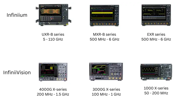 Fig 7. Keysight Infiniium and InfiniiVision oscilloscopes
This blog introduced several high-level aspects of oscilloscopes. Keysight provides a wide range of state-of-the-art, reliable, and proven oscilloscopes including real-time and equivalent-time scopes for lab use and handheld portable oscilloscopes for field use.
 MICHELLE TATE
Product Marketing
Keysight Technologies
The post An Overview of Oscilloscopes and Their Industrial Uses appeared first on ELE Times.
Best Virtual Machine Size for Self-Managed MongoDB on Microsoft Azure
Courtesy: Michał Prostko (Intel) and Izabella Raulin (Intel)
In this post, we explore the performance of MongoDB on Microsoft Azure examining various Virtual Machine (VM) sizes from the D-series as they are recommended for general-purpose needs.
Benchmarks were conducted on the following Linux VMs: Dpsv5, Dasv5, Dasv4, Dsv5, and Dsv4. They have been chosen to represent both the DS-Series v5 and DS-Series v4, showcasing a variety of CPU types. The scenarios included testing instances with 4 vCPUs, 8 vCPUs, and 16 vCPUs to provide comprehensive insights into MongoDB performance and performance-per-dollar across different compute capacities.
Our examination showed that, among instances with the same number of vCPUs, the Dsv5 instances consistently delivered the most favorable performance and the best performance-per-dollar advantage for running MongoDB.
MongoDB Leading in NoSQL Ranking
MongoDB stands out as the undisputed leader in the NoSQL Database category, as demonstrated by the DB-Engines Ranking. MongoDB emerges as the clear frontrunner in the NoSQL domain, with its closest competitors, namely Amazon DynamoDB and Databricks, trailing significantly in scores. Thus, MongoDB is supposed to maintain its leadership position.
MongoDB Adoption in Microsoft AzureEnterprises utilizing Microsoft Azure can opt for a self-managed MongoDB deployment or leverage the cloud-native MongoDB Atlas service. MongoDB Atlas is a fully managed cloud database service that simplifies the deployment, management, and scaling of MongoDB databases. Naturally, this convenience comes with additional costs. Additionally, it restricts us, for example, we cannot choose the instance type to run the service on.
In this study, the deployment of MongoDB through self-managed environments within Azure’s ecosystem was deliberately chosen to retain autonomy and control over Azure’s infrastructure. This approach allowed for comprehensive benchmarking across various instances, providing insights into performance and the total cost of ownership associated only with running these instances.
MethodologyIn the investigation into MongoDB’s performance across various Microsoft Azure VMs, the same methodology was followed as in our prior study conducted on the Google Cloud Platform. Below is a recap of the benchmarking procedures along with the tooling information necessary to reproduce the tests.
Benchmarking Software – YCSBThe Yahoo! Cloud Serving Benchmark (YCSB), an open-source benchmarking tool, is a popular benchmark for testing MongoDB’s performance. The most recent release of the YCSB package, version 0.17.0, was used.
The benchmark of MongoDB was conducted using a workload comprising 90% read operations and 10% updates to reflect, in our opinion, the most likely distribution of operations. To carry out a comprehensive measurement and ensure robust testing of system performance, we configured the YCSB utility to populate the MongoDB database with 10 million records and execute up to 10 million operations on the dataset. This was achieved by configuring the recordcount and operationcount properties within YCSB. To maximize CPU utilization on selected instances and minimize the impact of other variables such as disk and network speeds we configured each MongoDB instance with at least 12GB of WiredTiger cache. This ensured that the entire database dataset could be loaded into the internal cache, minimizing the impact of disk access. Furthermore, 64 client threads were set to simulate concurrency. Other YCSB parameters, if not mentioned below, remained as default.
SetupEach test consisted of a pair of VMs of identical size: one VM running MongoDB v7.0.0 designated as the Server Under Test (SUT) and one VM running YCSB designed as the load generator. Both VMs ran in the Azure West US Region as on-demand instances, and the prices from this region were used to calculate performance-per-dollar indicators.
ScenariosMongoDB performance on Microsoft Azure was evaluated by testing various Virtual Machines from the D-series, which are part of the general-purpose machine family. These VMs are recommended for their balanced CPU-to-memory ratio and their capability to handle most production workloads, including databases, as per Azure’s documentation.
The objective of the study is to compare performance and performance-per-dollar metrics across different processors for the last generation and its predecessor. Considering that the newer Dasv6 and Dadsv6 series are currently in preview, the v5 generation represents the latest generally available option. We selected five VM sizes that offer a substantively representative cross-section of choices in the general-purpose D-Series spectrum: Dsv5 and Dsv4 powered by Intel Xeon Scalable Processors, Dasv5 and Dasv4 powered by AMD EPYC processors, and Dpsv5 powered by Ampere Altra Arm-based processors. The testing scenarios included instances with 4, 8, and 16 vCPUs.
Challenges in VM type selection on AzureIn Microsoft Azure instances are structured in a manner where a single VM size can accommodate multiple CPU families. This means that different VMs created under the same VM Size can be provisioned on different CPU types. Azure does not provide a way to specify the desired CPU during instance creation, neither through the Azure Portal nor API. The CPU type can only be determined once the instance is created and operational from within the operating system. It turned out that it required multiple tries to get matching instances as we opted for an approach where both the SUT and the client instance have the same CPU type. What was observed is that larger instances (with more vCPUs) tended to have newer generations of CPU more frequently, while smaller instances were more likely to have the older ones. Consequently, for the smaller instances of Dsv5 and Dsv4 we have never come across VMs with 4th Generation Intel Xeon Scalable Processors.
More details about VM sizes used for testing are provided in Appendix A. For each scenario, a minimum of three runs were conducted. If the results showed variations exceeding 3%, an additional measurement was taken to eliminate outlier cases. This approach ensures the accuracy of the final value, which is derived from the median of these three recorded values.
ResultsThe measurements were conducted in March 2024, with Linux VMs running Ubuntu 22.04.4 LTS and kernel 6.5.0 in each case. To better illustrate the differences between the individual instance types, normalized values were computed relative to the performance of the Dsv5 instance powered by the 3rd Generation Intel Xeon Scalable Processor. The raw results are shown in Appendix A.
Whether both 16 vCPUs Dsv4 and Dsv5 VMs are powered by 3rd Generation Intel Xeon Scalable Processors 8370C and, moreover, they share the same compute cost of $654.08/month, the discrepancy in MongoDB workload performance scores is observed, favoring the Dsv5 instance. This difference can be attributed to the fact that the tested 16 vCPUs Dsv4, as a representation of the 4th generation of D-series, is expected to be more aligned with other representatives of its generation (see Table 1). Analyzing results for Dasv4 VMs vs Dasv5 VMs, powered by 3rd Generation AMD EPYC 7763v, similar outcomes can be noted – in each tested case, Dasv5-series VMs overperformed Dasv4-series VMs.
Observations:- Dsv5 VMs, powered by 3rd Generation Intel Xeon Scalable Processor, offer both the most favorable performance and the best performance-per-dollaramong the other instances tested in each scenario (4vCPUs, 8vCPUs, and 16 vCPUs).
- Dasv5 compared to Dsv5 is less expensive, yet it provides lower performance. Therefore, the Total Cost of Ownership (TCO) is in favour of the Dsv5 instances.
- Dpsv5 VMs, powered by Ampere Altra Arm-based processors, have the lowest costs among the tested VM sizes. However, when comparing performance results, that type of VM falls behind, resulting in the lowest performance-per-dollar among the tested VMs.
The presented benchmark analysis covers MongoDB performance and performance-per-dollar across 4vCPUs, 8vCPUs, and 16 vCPUs instances representing general-purpose family VM sizes available on Microsoft Azure and powered by various processor vendors. Results show that among the tested instances, Dsv5 VMs, powered by 3rd Generation Intel Xeon Scalable Processors, provide the best performance for the MongoDB benchmark and lead in performance-per-dollar.
Appendix A
The post Best Virtual Machine Size for Self-Managed MongoDB on Microsoft Azure appeared first on ELE Times.
An Introduction to Several Commonly used AFEs and their Schemes
Courtesy: Infineon
This article will introduce you to the development of new energy vehicles and energy storage industry, several ways of cell collection solutions, and focus on Infineon’s new AFE acquisition chip TLE9018DQK as well as its use and technical characteristics.
In terms of passenger cars, in recent years, with the emergence of a new round of scientific and technological revolution and industrial transformation, the new energy vehicle industry has entered a stage of accelerated development. China’s new energy vehicle industry, after years of continuous efforts, the technical level has been significantly improved, the industrial system has been improved, and the competitiveness of enterprises has been greatly enhanced, showing a good situation of “double improvement” of market scale and development quality.
In terms of energy storage, electrochemical energy storage, as the fastest growing energy storage method in recent years, has rapidly increased from 3.7% in 2018 to 7.5% in 2020. Lithium-ion battery energy storage has high energy density, wide commercial application, declining unit cost, and mature technology, so lithium-ion battery energy storage has become the hegemon of global electrochemical energy storage. According to the data, by the end of 2020, lithium-ion batteries accounted for 92% of the installed capacity of electrochemical energy storage, and sodium-sulfur batteries and lead-acid batteries accounted for 3.6% and 3.5%, respectively. At present, lithium-ion energy storage mainly uses lithium iron phosphate battery technology.
2. Introduction to the collection plan (1) Cell collection realized by AD chipWhether it is new energy passenger vehicles or energy storage, new requirements and standards have been put forward for the BMS industry. A key technology in BMS technology is the collection and protection of cell parameters, the so-called AFE technology. In the early days, there were no AFE chips, and the collection of battery cells was basically collected one by one with AD chips. The electronic switch is used to achieve the purpose of sequential switching. The scheme is roughly as follows:
As shown in the figure above, its principle is to use 2 electronic switches, at the same time, the upper switch strobe one way, and the lower switch strobe one way, (the electronic switch adopts TI’s MUX5081DR, and which one gated is configured through 3 addresses). During the switching process, ensure that the strobe of the upper switch and the lower switch are adjacent to each other, and the strobe of the upper switch is the high position. The gated two-way data is collected differentially through ADI’s ADS1113IDGSR and converted into an I2C signal for MCU communication.
The acquisition rate and accuracy of this collection method are not very high, and the general acquisition accuracy must reach 14 bits to meet the requirements of cell collection. This collection method is currently used in the collection of some special cells, such as nickel-chromium, nickel-metal hydride, and lead-acid batteries. Because most of the cells in this concentration appear in groups. Most of us use this group as a cell to deal with, and the voltage of this group will generally be greater than 5V, such as the 12V of the lead-acid group that we are familiar with. This is where this approach is needed to achieve partial pressure harvesting.
(2) Cell protection achieved by a single-cell cell protection chipThere is also a simple single-cell collection scheme on the market, which features that each cell is independently protected by a single chip. As shown in the figure below:
The chip HY2112-BB can realize the protection of over-voltage and over-under-voltage, charging detection and charge-discharge control. The operation mode is mainly realized by driving the external MOS with the drive pin of the output.
(3) Cell protection realized by multi-cell cell protection chipsThere are mainly 4 strings, 7 strings, 8 strings, 12 strings, 14 strings, and 16 strings of multi-cell acquisition chips on the market. Among them, 12 strings and 14 strings are the majority. Typical examples are ADI’s LTC6803HG and NXP’s MC33771A.
As shown in the figure below:
Figure 3 shows BYD’s 4-string BM3451 acquisition chip scheme. Figure 4 shows ADI’s 12-string LTC6803HG acquisition scheme, and Figure 5 shows NXP’s 14-string MC33771 acquisition scheme.
In addition to cell voltage acquisition, noise filtering, self-function monitoring, and integrated internal equalization MOS, these two types of acquisition also have multi-channel temperature acquisition, and MC33771 also comes with internal current measurement, simplifying the BMS current acquisition loop.
 Fig.4 Acquisition scheme of LTC6803HG
3. Infineon’s new TLE9018DQK AFE acquisition solution
Infineon’s AFE acquisition solution is mainly TLE9012 in the early stage, and compared with other chips, the most important feature of this chip is the integrated pressure and temperature compensation function. This function enables the chip to maintain good acquisition accuracy in special environments. The main disadvantage is that the number of strings is relatively small, and there are limitations in the combination of strings and combinations. The TLE9018DQK is developed on the basis of TLE9012, and its functional characteristics are mainly as follows:
1. It can monitor 18 strings of batteries at the same time.
2. The maximum voltage can reach 120V, with strong ESD function. It can support frontal hot swapping without external protection (due to its high withstand voltage value and internal protection).
3. Integrated stress sensor and temperature compensation with digital compensation algorithm. Its products can maintain high acquisition accuracy in a variety of complex environments.
4. Integrated 8 temperature acquisition channels.
5. The maximum passive equalization circuit can reach 300mA.
6. Support capacitive coupling and transformer coupling in communication.
7. It has multiple wake-up sources, so it can wake up the chip in a variety of ways.
8. With automatic no-load detection function.
The peripheral pinout diagram looks like this:
TLE9018DQK is suitable for HEV, PHEV, BEV, energy storage and other product applications. The package form is: PG-FQLP-64. The maximum permissible temperature range is –40-150°C. The comparison of TLE9018 with other chip technical parameters can be referred to the following figure:
Here, for TLE9018DQK, a set of cell collection schemes is made, as shown in the figure below.
Because the TLE9018DQK has its own passive balancing MOS, the external balancing circuit only needs to be connected to the current-limiting resistor, and considering the resistor power problem under the maximum balancing current, two 82R, package 2512 power resistors are connected in parallel to improve reliability. The 8-channel temperature measurement is delivered to the MCU with a 3.3K current-limiting resistor. External 100K NTC temperature sensor for temperature collection. If the temperature sensor is not used so much, the unused pins must be pulled down to the ground end.
IFL_L, IFL_H, IFH_L, IFH_H, and four pins are externally connected to Infineon’s isolated communication chip TLE9015, which can realize multi-level series daisy-chain communication.
The ERR pin is connected directly to the MCU and can feed back the current state of the chip to the MCU.
The chip comes with 4 GPIO pins, which can control external indicators, alarms, etc., which are not used here for the time being, so they are directly pulled down to ground.
The post An Introduction to Several Commonly used AFEs and their Schemes appeared first on ELE Times.

