
ELE Times

Vishay Intertechnology Gen 4.5 650 V E Series Power MOSFET Delivers Industry’s Lowest RDS(ON)*Qg and RDS(ON)*Co(er) FOMs
Superjunction Device Enables High Power Ratings and Density While Lowering Conduction and Switching Losses to Increase Efficiency
Vishay Intertechnology, Inc. introduced a new Gen 4.5 650 V E Series power MOSFET that delivers high efficiency and power density for telecom, industrial, and computing applications. Compared to previous-generation devices, the Vishay Siliconix n-channel slashes on-resistance by 48.2 % while offering a 65.4 % lower resistance times gate charge, a key figure of merit (FOM) for 650 V MOSFETs used in power conversion applications.
Vishay offers a broad line of MOSFET technologies that support all stages of the power conversion process, from high voltage inputs to the low voltage outputs required to power the latest high tech equipment. With the SiHK050N65E and other devices in the Gen 4.5 650 V E Series family, the company is addressing the need for efficiency and power density improvements in two of the first stages of the power system architecture — power factor correction (PFC) and subsequent DC/DC converter blocks. Typical applications will include servers, edge computing, and super computers; UPS; high intensity discharge (HID) lamps and fluorescent ballast lighting; telecom SMPS; solar inverters; welding equipment; induction heating; motor drives; and battery chargers.Built on Vishay’s latest energy-efficient E Series superjunction technology, the SiHK050N65E’s low typical on-resistance of 0.048 Ω at 10 V results in a higher power rating for applications > 6 kW. With 50 V of additional breakdown voltage, the 650 V device addresses 200 VAC to 277 VAC input voltages and the Open Compute Project’s Open Rack V3 (ORV3) standards. In addition, the MOSFET offers ultra low gate charge down to 78 nC. The resulting FOM of 3.74 Ω*nC translates into reduced conduction and switching losses to save energy and increase efficiency. This allows the device to address the specific titanium efficiency requirements in server power supplies or reach 96 % peak efficiency.
The post Vishay Intertechnology Gen 4.5 650 V E Series Power MOSFET Delivers Industry’s Lowest RDS(ON)*Qg and RDS(ON)*Co(er) FOMs appeared first on ELE Times.
Upgraded sensor board from STMicroelectronics accelerates plug-and-play evaluation with ST MEMS Studio
New hardware integrates closely with convenient, graphical development environment
Developing context-aware applications with MEMS sensors is faster, more powerful, and more flexible with ST’s latest-generation sensor evaluation board, the STEVAL-MKI109D. Now upgraded with an STM32H5 microcontroller, USB-C connector, and extra digital interfaces including I3C for flexible communication, the new board lets users quickly evaluate sensors and confidently handle demanding projects.
Engineers unveiled the STEVAL-MKI109D during a live tech lab, showing how to simply plug in a sensor module, connect a PC, and start analyzing data in ST MEMS Studio. Using this all-in-one graphical environment, developers can visualize the sensor output, quickly fine-tune settings, configure features, and exercise the AI capabilities of ST sensors with a machine-learning core (MLC) and intelligent sensor processing unit (ISPU) inside. The tool provides advanced functions including power monitoring and supply voltage management that help optimize energy consumption and debugging.
ST’s MEMS portfolio contains inertial sensors, pressure sensors, biosensors, and digital and analog microphones offering many choices of speed, accuracy, full-scale range, and package style in industrial, consumer, and automotive grades. Extremely compact and robust, they are suited to diverse applications including consumer products, smartphones, wearables, smart-home devices, industrial sensing, safety equipment, healthcare, environmental monitoring, and many more. Automotive-grade devices target applications including navigation support, advanced driver assistance, and automated driving.
An evaluation module is available for each sensor type, mounted on a convenient DIL24 card with headers, ready to connect to the STEVAL-MKI109D board. Additional plug-and-play accessories are available, including biosensor electrodes and remote-sensing extension cables to quickly evaluate sensors when building proof-of-concept models and developing prototypes.
The STM32H5 MCU at the heart of the new board has the latest high-performing and efficient Arm Cortex-M33 core with extensive peripherals that enable faster, more convenient development. Customers’ sensor projects can target any of the over 1400 microcontrollers and microprocessors in the STM32 family. The MLC, finite-state machine (FSM), and ISPU embedded in select MEMS devices help optimize application performance and power consumption for superior functionality, responsiveness, and battery runtime.
The STEVAL-MKI109D board is available from distributors and the eSTore, from $105. ST MEMS Studio is ready to download now at www.st.com/mems-studio and is supported with automatic upgrades to ensure users always have the latest software and firmware.
For further information please visit: www.st.com/mems-studio
The post Upgraded sensor board from STMicroelectronics accelerates plug-and-play evaluation with ST MEMS Studio appeared first on ELE Times.
PolarFire SoC FPGAs Achieve AEC-Q100 Qualification
The robust, low-power solutions from Microchip Technology meet stringent automotive standards for reliability in harsh conditions
Microchip Technology’s PolarFire System on Chip (SoC) FPGAs have earned the Automotive Electronics Council (AEC)-Q100 qualification. The AEC-Q standards are a guideline for integrated circuits, using stress tests to measure the reliability of electronic components in vehicles. AEC-Q100 qualified devices have gone through rigorous testing to demonstrate they can withstand extreme conditions in automotive applications.
The PolarFire SoC FPGA has been qualified for automotive Grade 1 temperatures, -40°C to 125°C. PolarFire SoC FPGAs feature an embedded 64-bit, quad-core RISC-V architecture capable of running Linux and real-time operating systems (RTOS), with mid-range density programmable logic of up to 500K logic elements (LE). The SoC FPGA is designed for complex applications that demand low-power, high-performance, exceptional reliability and an extended operating temperature range. Devices with the same density and package have scalable assurance and share pin-package compatibility across temperature grades, making it appropriate for automotive use as well as aerospace and military applications.
The SoC FPGAs incorporate embedded security and safety features to protect physical, device, design and data integrity. The SoCs are designed with single event upset (SEU) immunity, which enhances reliability and helps mitigate the risk of data corruption and system failures in demanding environments.
“Achieving the AEC-Q100 qualification for our PolarFire SoC FPGAs validates that our technology can perform under the most challenging conditions and underscores our commitment to delivering robust solutions to meet the stringent demands of the automotive industry,” said Bruce Weyer, Corporate Vice President of Microchip’s FPGA business unit. “Our low-power design and RISC-V cores empower automotive engineers to create advanced, reliable and energy-efficient solutions for next-generation automotive systems.”
PolarFire FPGAs and SoCs deliver power and thermal efficiency, eliminating the need for active cooling while ensuring high integration, defense-grade security and reliability. With high levels of scalability, they maintain performance across varying temperature conditions and meet stringent demands of mission-critical environments.
Development Tools
PolarFire SoCs are supported by Microchip’s Libero SoC Design Suite, SmartHLS, VectorBlox and Microchip’s Mi-V ecosystem of partner platforms for rapid RISC-V application development. Additionally, a wide variety of Microchip and partner intellectual property (IP) cores are available to accelerate time-to-market. Libero SoC Design Suite is TÜV Rheinland-certified for functional safety, meeting ISO 26262 ASIL D standards for automotive applications. Compatible development boards are also available.
The post PolarFire SoC FPGAs Achieve AEC-Q100 Qualification appeared first on ELE Times.
From Assembly to Innovation: India’s Transformative Mobile Manufacturing Revolution
The Indian mobile manufacturing landscape represents a remarkable narrative of technological transformation, economic strategy, and industrial innovation. What was once a predominantly import-driven market has metamorphosed into a robust domestic production powerhouse, driven by a confluence of governmental initiatives, technological investments, and strategic corporate vision.
Xiaomi India: A Manufacturing Paradigm ShiftXiaomi’s journey in India epitomizes the potential of localized manufacturing. Their production facilities in Chennai and Noida are not merely assembly lines but sophisticated technological ecosystems that represent the cutting edge of mobile manufacturing. The company has systematically invested in creating a comprehensive manufacturing infrastructure that goes beyond simple assembly.
The technological sophistication of Xiaomi’s manufacturing approach is evident in their deployment of advanced Surface Mount Technology (SMT) lines. These highly automated production systems enable precision component placement, ensuring consistent quality and minimizing human error. Robotic assembly processes have been integrated to enhance production efficiency, allowing for rapid scaling and maintaining stringent quality standards.
Moreover, Xiaomi’s local sourcing strategy has been instrumental in creating a robust domestic supply chain. By strategically partnering with local component manufacturers and investing in local ecosystem development, they have not just reduced production costs but also contributed to developing India’s electronics manufacturing capabilities.
Samsung: A Global Manufacturing Powerhouse in IndiaSamsung’s manufacturing complex in Noida represents more than just a production facility – it is a testament to advanced manufacturing capabilities. The facility stands as one of the world’s largest mobile phone factories, embodying cutting-edge technological integration and precision engineering.
The company’s approach transcends traditional manufacturing paradigms. Advanced Printed Circuit Board (PCB) manufacturing techniques, coupled with comprehensive quality assurance protocols, ensure that every device meets global standards. Their laboratories represent technological sanctuaries where each component undergoes rigorous testing, examining everything from thermal performance to electromagnetic compatibility.
Samsung’s integrated design and production workflows demonstrate a holistic approach to mobile manufacturing. By seamlessly connecting research, design, and production departments, they create an ecosystem that rapidly translates technological innovations into market-ready products.
Emerging Players: Realme and the New Manufacturing ParadigmRealme represents the new generation of mobile manufacturers – agile, technology-driven, and deeply committed to localization. Their manufacturing facilities in Greater Noida are not just production centers but innovation laboratories that embrace modern manufacturing philosophies.
Lean manufacturing principles guide their production strategy, allowing for maximum efficiency and minimal waste. Modular production designs enable rapid prototyping and quick adaptation to market demands. This approach allows Realme to maintain a competitive edge in a rapidly evolving market, responding swiftly to technological trends and consumer preferences.
Oppo and Vivo: Synchronized Manufacturing ExcellenceThe sister companies Oppo and Vivo have developed a synchronized manufacturing ecosystem that exemplifies technological sophistication. Their facilities in Greater Noida and Noida are equipped with state-of-the-art automated optical inspection systems, ensuring that every device meets exacting quality standards.
Their manufacturing approach integrates advanced thermal and durability testing, recognizing that modern smartphones must withstand diverse environmental conditions. Comprehensive supply chain integration ensures that each component is not just sourced but meticulously validated.
Apple’s Strategic Manufacturing PresenceThough not an Indian company, Apple’s manufacturing strategy through Foxconn and Wistron represents a significant milestone in India’s mobile manufacturing journey. The facilities in Chennai and Bengaluru showcase precision engineering workflows that align with global high-end smartphone production standards.
Technological Horizons and Future TrajectoriesThe Indian mobile manufacturing ecosystem is poised at an exciting technological frontier. Emerging trends point towards deeper 5G component localization, advanced semiconductor integration, and AI-driven manufacturing optimization. Sustainability is becoming a critical consideration, with manufacturers exploring eco-friendly production technologies.
Government’s Transformative RoleThe Production Linked Incentive (PLI) scheme has been the catalyst that transformed potential into reality. By creating a supportive policy environment, the government has not just attracted investments but fundamentally reshaped India’s technological manufacturing landscape.
Conclusion: A Global Manufacturing DestinationIndia’s mobile manufacturing journey is a narrative of technological ambition, strategic vision, and relentless innovation. From being a consumer market to emerging as a global manufacturing hub, the transformation is profound and promising.
The road ahead is illuminated by continuous technological advancement, strategic investments, and an unwavering commitment to excellence.
The post From Assembly to Innovation: India’s Transformative Mobile Manufacturing Revolution appeared first on ELE Times.
Understanding Gold Soldering: Definition, Process, Working, Uses & Advantages
Gold soldering is a sophisticated metallurgical joining technique that represents the pinnacle of precision manufacturing processes. Unlike conventional soldering methods, this specialized technique involves creating permanent, high-integrity connections between gold or gold-alloy components with exceptional precision and reliability. The process goes beyond simple mechanical joining, instead creating a deep metallurgical bond that ensures optimal electrical, thermal, and structural performance.
How Gold Soldering WorksThe scientific principles underlying gold soldering are complex and multifaceted. At its core, the process involves creating an atomic-level bond between gold surfaces using a carefully selected filler material with a strategically lower melting point. The metallurgical interaction is not merely a surface-level connection but a profound interdiffusion of metal atoms that creates a seamless, integrated joint.
The fundamental mechanism begins with the careful preparation of surfaces, where even microscopic contaminants can compromise the entire soldering process. As the filler material is heated, it transitions from a solid to a liquid state, simultaneously wetting the gold surfaces and creating a capillary action that draws the molten material between the components. During this process, atomic diffusion occurs, where the atoms of the filler material intermingle with the gold surfaces, creating a bond that is often stronger and more reliable than the original base materials.
Gold Soldering ProcessSurface Preparation: The Critical First Step
Surface preparation is arguably the most crucial phase of gold soldering. This stage requires meticulous attention to detail and advanced cleaning techniques. Professionals employ a combination of chemical and mechanical methods to eliminate any potential contaminants. Specialized solvents are used to remove organic residues, while precise chemical etching or plasma cleaning techniques eliminate oxide layers and microscopic impurities.
The goal is to create an absolutely pristine surface that allows for maximum metallurgical interaction. Even a thin layer of oxidation or a microscopic particle can prevent proper bonding, leading to weak joints or complete soldering failure. Advanced cleaning techniques may include ultrasonic cleaning, chemical degreasing, and high-precision surface treatments that can remove contaminants at the atomic level.
Material Selection: A Delicate Science
Selecting the appropriate materials is a complex process that requires deep understanding of metallurgical properties. The gold alloy composition must be carefully matched with an appropriate filler material that can create a reliable bond while maintaining the desired mechanical and electrical properties. Factors such as melting point, thermal expansion coefficient, and chemical compatibility are meticulously evaluated.
Different applications demand different material characteristics. For instance, electronics may require a filler material that provides optimal electrical conductivity, while medical devices might prioritize biocompatibility and corrosion resistance. This selection process often involves extensive material testing and simulation to ensure optimal performance under various operational conditions.
Uses & ApplicationsElectronics Industry: Pushing Technological Boundaries
In the electronics industry, gold soldering is nothing short of revolutionary. Semiconductor packaging relies on this technique to create microscopic connections that form the backbone of advanced electronic devices. Hybrid microelectronics, which combine different types of electronic components, depend entirely on the precision and reliability of gold soldering techniques.
Modern smartphones, advanced medical imaging equipment, and cutting-edge aerospace technologies all benefit from gold soldering’s ability to create miniaturized, high-performance connections. The technique allows for the integration of components at nanoscale levels, enabling technological advancements that were previously impossible.
Medical and Aerospace Applications: Reliability in Extreme Conditions
In medical and aerospace domains, gold soldering’s reliability becomes paramount. Implantable medical devices require connections that can withstand the human body’s complex chemical environment, while aerospace components must endure extreme temperature variations and intense radiation.
The ability to create stable, corrosion-resistant joints makes gold soldering indispensable in these critical fields. Precision surgical instruments, satellite communication systems, and advanced sensor technologies all rely on the unique properties that gold soldering provides.
Advantages and ChallengesGold soldering offers remarkable advantages, including exceptional conductivity, corrosion resistance, and the ability to create extremely precise connections. However, these benefits come with significant challenges. The process is inherently expensive, requiring specialized equipment and highly trained professionals.
The narrow temperature window for optimal soldering demands extraordinary skill and precision. A deviation of mere degrees can compromise the entire soldering process, making it a technique that requires continuous training and technological investment.
ConclusionGold soldering represents more than just a joining technique—it is a sophisticated technology that pushes the boundaries of what is possible in manufacturing. As technological demands become increasingly complex, the importance of this precise metallurgical process will only continue to grow.
Professionals in electronics, medical technology, aerospace, and advanced manufacturing must continually invest in understanding and mastering these intricate soldering techniques to drive technological innovation forward.
The post Understanding Gold Soldering: Definition, Process, Working, Uses & Advantages appeared first on ELE Times.
Spintronics and Magnetoelectric RAM: A Comprehensive Technical Exploration
- Fundamental Quantum Mechanical Foundations
1.1 Quantum Spin Dynamics
Spintronics represents a revolutionary paradigm that fundamentally challenges traditional electronic technologies by exploiting the quantum mechanical spin property of electrons. Unlike conventional charge-based electronics, spin-based technologies leverage the intrinsic angular momentum of electrons, characterized by two quantum states: spin-up (|↑⟩) and spin-down (|↓⟩). This binary quantum nature provides an unprecedented foundation for information storage and processing, opening new frontiers in computational architecture.
The mathematical representation of spin dynamics is elegantly captured by the Heisenberg Hamiltonian:
H = -∑(J_ij * S_i · S_j)
This equation encapsulates the quantum mechanical interaction between spin operators, where J_ij represents the exchange coupling constant, and S_i and S_j describe spin operators at specific lattice sites. The fundamental interaction demonstrates the complex quantum mechanical spin correlation mechanisms that underpin spintronic technologies.
1.2 Spin-Orbit Coupling Phenomena
Spin-orbit coupling (SOC) emerges as a critical quantum mechanical interaction where an electron’s spin precession becomes intrinsically coupled with its orbital motion. This phenomenon introduces sophisticated spin-dependent electronic transport mechanisms that are crucial for advanced spintronic devices.
The field of spin-orbit coupling encompasses several profound physical manifestations. The Rashba effect represents a quantum mechanical spin splitting mechanism primarily observed in two-dimensional electron systems with broken inversion symmetry. This effect generates a spin-momentum locking phenomenon where electron spin becomes intrinsically linked to its momentum direction, creating unique quantum transport behaviors.
The Dresselhaus effect complements the Rashba mechanism, representing a bulk spin-orbit coupling phenomenon prevalent in non-centro-symmetric crystal structures. Originating from bulk inversion asymmetry, this effect generates spin-dependent electron scattering mechanisms that fundamentally deviate from traditional electronic transport models.
- Magnetoelectric RAM: Advanced Architectural Insights
2.1 Magnetoelectric Coupling Mechanisms
Magnetoelectric RAM (MeRAM) represents a sophisticated memory paradigm that exploits the intricate coupling between magnetic and ferroelectric materials. The fundamental interaction can be described by a phenomenological free energy expression:
F = F_magnetic + F_electric + F_magnetoelectric
This sophisticated approach enables electric-field-induced magnetic state modulation with unprecedented precision, bridging quantum mechanical principles with advanced computational memory technologies.
The material design for effective magnetoelectric RAM demands a nuanced approach to material selection and interface engineering. Critical material characteristics include the magnetoelectric coefficient (α_ME), which quantifies the material’s ability to couple magnetic and electric polarization states. Magnetic anisotropy energy plays a crucial role in determining the stability of magnetic configurations, while ferroelectric polarization magnitude determines the efficiency of electric-field-based switching mechanisms.
2.2 Magnetic Tunnel Junction (MTJ) Architectures
Magnetic Tunnel Junctions (MTJs) represent the core computational element in MeRAM, utilizing quantum mechanical tunneling phenomena for information storage and transfer. The typical MTJ multilayer configuration consists of carefully engineered ferromagnetic electrodes separated by an ultrathin insulating barrier, enabling sophisticated quantum mechanical information processing.
- Advanced Quantum Transport Mechanisms
3.1 Spin-Transfer Torque (STT)
Spin-transfer torque emerges as a sophisticated quantum mechanical mechanism for manipulating magnetic moments through spin-polarized current injection. The Landau-Lifshitz-Gilbert-Slonczewski (LLGS) equation provides a comprehensive mathematical framework for describing the complex magnetization dynamics inherent in this mechanism.
The quantum mechanical principles involve direct momentum transfer from spin-polarized electrons to magnetic moments within a material system. When a spin-polarized current passes through a magnetic multilayer structure, electron spins interact with local magnetic moments, exerting a torque that can rotate or manipulate the magnetic configuration with unprecedented precision.
3.2 Magnetoelectric Switching Dynamics
Electric-field-induced magnetic switching represents a pinnacle of quantum mechanical interface engineering. This sophisticated mechanism transcends traditional electronic switching by directly manipulating magnetic states through electric field application.
The underlying physics encompasses multiple interrelated quantum mechanical phenomena, including strain-mediated magnetic coupling, direct exchange interactions, and interfacial charge redistribution mechanisms. These complex interactions enable precise control of magnetic configurations through electrical means, representing a quantum leap in computational memory technologies.
- Performance Characterization and Metrics
4.1 Advanced Performance Parameters
The evaluation of magnetoelectric RAM technologies requires a multidimensional approach that extends beyond traditional memory performance metrics. Key performance indicators include:
- Energy Consumption: Targeting switching energies below 0.1 picojoules per bit
- Write Latency: Approaching near-ballistic regime switching speeds of a single nanosecond
- Data Retention: Targeting retention times exceeding decade-long scales
- Endurance: Approaching or exceeding 10^12 write operations
4.2 Thermal Stability Considerations
Thermal stability represents a fundamental challenge in advanced memory technologies. The Arrhenius equation provides a mathematical framework for understanding magnetic state lifetime, relating it to material-specific energy barriers and operational temperatures.
- Material Science Innovations
5.1 Emerging Magnetoelectric Materials
The frontier of MeRAM technologies hinges on material science innovations that push quantum mechanical engineering boundaries. Key approaches include:
- Multiferroic composites combining ferromagnetic and ferroelectric properties
- Engineered heterogeneous interfaces with atomically precise boundaries
- Topological magnetic materials providing inherent quantum decoherence protection
- Rare-earth metal substitutions enabling fine-tuned material properties
5.2 Nanostructuring Techniques
Advanced nanostructuring methodologies include:
- Molecular beam epitaxy (MBE) for atomic-layer-precise material deposition
- Pulsed laser deposition for creating complex material architectures
- Focused ion beam lithography for nanoscale structural modifications
- Atomic layer deposition (ALD) for ultra-thin, precisely controlled material layers
- Industry and Research Implications
6.1 Technological Disruption Potential
MeRAM technologies offer transformative capabilities across multiple domains:
- High-performance computing with extraordinary energy efficiency
- Internet of Things (IoT) devices with ultra-low power consumption
- Neuromorphic computing architectures mimicking biological neural networks
- Bridging classical and quantum computational paradigms
6.2 Economic and Computational Impacts
- Projected market value: $500 million by 2028
- Potential 70% reduction in computational energy consumption
- Enabling more sustainable and efficient computing infrastructures
Spintronics and MeRAM represent a quantum leap in computational memory technologies, bridging fundamental quantum mechanical principles with advanced engineering methodologies. By leveraging sophisticated quantum mechanical interactions, these technologies promise to revolutionize computational architectures, offering unprecedented performance, energy efficiency, and computational capabilities.
Disclaimer: Technological developments are ongoing, and specific implementations may vary.
The post Spintronics and Magnetoelectric RAM: A Comprehensive Technical Exploration appeared first on ELE Times.
Selective Soldering: Definition, Process, Working, Uses & Advantages
Selective soldering is an advanced soldering technique used in electronics manufacturing to solder specific components on a printed circuit board (PCB) without affecting adjacent parts. Unlike traditional wave soldering, which exposes the entire board to molten solder, selective soldering focuses only on designated areas, making it ideal for complex PCB assemblies with mixed technology components.
This method is essential in industries where high precision and reliability are required, such as aerospace, automotive, medical devices, and telecommunications. Selective soldering helps manufacturers meet stringent quality standards while reducing thermal stress on sensitive components.
How Selective Soldering WorksSelective soldering involves applying molten solder to specific areas of the PCB using a programmable system. It typically follows these key steps:
- Flux Application: A controlled amount of flux is selectively applied to solder joints to improve wetting and prevent oxidation.
- Preheating: The PCB is preheated to activate the flux and reduce thermal shock, ensuring better solder flow.
- Soldering Process: A programmable soldering nozzle or mini-wave applies molten solder to the designated areas, forming high-quality solder joints.
- Cooling and Inspection: The board is cooled down gradually, and automated inspection methods such as X-ray or AOI (Automated Optical Inspection) are used to ensure quality.
The selective soldering process can be categorized into three main techniques:
- Mini-Wave Soldering
This method involves using a small nozzle that creates a miniature solder wave, selectively soldering through-hole components. The PCB moves over the wave, allowing precise solder application.
- Jet Wave Soldering
In this approach, a high-precision nozzle dispenses solder in a controlled manner. It is ideal for densely populated PCBs where precise control is required.
- Laser Selective Soldering
This technique utilizes a laser to heat the solder and create joints without physical contact. It is beneficial for highly sensitive components that require minimal thermal exposure.
Each of these methods is chosen based on factors such as board complexity, component density, and production volume.
Selective Soldering Uses & ApplicationsSelective soldering is widely used across various industries due to its precision and reliability. Some of the primary applications include:
- Automotive Electronics: Used in engine control units (ECUs), infotainment systems, and safety modules where high-reliability soldering is required.
- Aerospace and Defense: Essential for high-reliability PCBs used in avionics and military communication systems.
- Medical Devices: Applied in medical instrumentation where strict quality standards are necessary.
- Consumer Electronics: Used in complex PCB assemblies for smartphones, tablets, and wearables.
- Industrial Automation: Ensures robust connections in industrial control systems and robotics.
- Precision and Selectivity
Selective soldering allows targeted soldering, reducing the risk of damage to nearby components. This is particularly useful for mixed-technology PCBs.
- Reduced Thermal Stress
Unlike wave soldering, which exposes the entire board to heat, selective soldering minimizes thermal exposure, protecting heat-sensitive components.
- Higher Reliability
With precise solder control, the process ensures consistent joint quality, reducing defects such as solder bridges or cold joints.
- Cost-Effectiveness
Selective soldering reduces solder and flux consumption while minimizing rework and scrap rates, leading to cost savings in production.
- Automation Compatibility
Modern selective soldering systems can be fully automated, improving repeatability and efficiency in high-volume manufacturing.
Selective Soldering Disadvantages- Slower Process Compared to Wave Soldering
Since each component is soldered individually, the process is slower than wave soldering, making it less ideal for extremely high-volume production.
- Higher Initial Investment
Selective soldering machines are more expensive compared to traditional soldering equipment, requiring a significant upfront investment.
- Complex Programming and Setup
Proper setup and programming are required to achieve optimal results, necessitating skilled operators and additional setup time.
ConclusionSelective soldering is a vital technique in modern electronics manufacturing, providing high precision, reliability, and cost-efficiency. While it has certain limitations, its advantages make it indispensable for industries requiring robust and precise soldering solutions. As technology advances, selective soldering is expected to become even more efficient, further enhancing its role in electronic assembly processes.
The post Selective Soldering: Definition, Process, Working, Uses & Advantages appeared first on ELE Times.
Understanding Wire Soldering: Definition, Process, Working, Uses & Advantages
Wire soldering is a fundamental technique in electronics and electrical engineering that involves joining two or more metal wires using a filler metal, known as solder. This process ensures a strong, conductive, and durable connection between components. Soldering is widely used in circuit board assembly, electrical wiring, and microelectronics, offering a reliable means of creating robust electrical and mechanical bonds.
What is Wire Soldering?Wire soldering is a method of joining electrical wires and components by melting a filler metal (solder) at the joint. The solder, typically composed of a lead-tin alloy or a lead-free alternative, melts at a lower temperature than the workpieces, allowing it to flow and solidify, creating a permanent bond. The process ensures excellent electrical conductivity and mechanical strength, making it essential in various industrial and DIY applications.
How Wire Soldering WorksWire soldering works on the principle of wetting and capillary action. Temperature control plays a critical role, as solder melts at specific temperatures, typically 180–200°C for tin-lead solder and 217°C for lead-free solder. Proper heat application ensures strong joints and prevents damage to sensitive electronic components. The use of flux is essential in wire soldering, as it removes oxidation and improves adhesion by enhancing the flow of solder and preventing contaminants from interfering with the bond. Surface preparation is another crucial factor, as clean wire surfaces result in stronger solder joints. Any contaminants like oxidation or dirt can weaken the bond and should be removed before soldering. Additionally, the cooling rate must be managed properly. Gradual cooling prevents joint brittleness and ensures a reliable bond, whereas sudden cooling may introduce stress and weak points in the joint.
Wire Soldering ProcessThe wire soldering process consists of several key steps to ensure a high-quality joint. The first step is preparation, where essential tools such as a soldering iron, solder wire, flux, helping hands or clamps, and wire strippers are gathered. The wire surfaces must be cleaned with alcohol or a wire brush to remove oxidation and dirt, and flux should be applied to improve solder flow and reduce oxidation.
The next step is heating the joint. The soldering iron must be heated to the required temperature, typically between 300–400°C depending on the type of solder being used. The iron tip should be placed in contact with both wires to ensure even heating before applying solder. Once the joint reaches the correct temperature, solder is applied. The molten solder should flow into the joint via capillary action, forming a strong bond. The soldering process should be completed quickly to prevent excessive heat damage to components. The final step is cooling and inspection. The joint must be allowed to cool naturally without disturbance to maintain structural integrity. A visual and mechanical inspection should be performed to ensure proper bonding and electrical continuity.
Wire Soldering Uses & ApplicationsWire soldering finds applications in various industries due to its reliability and efficiency. In the electronics and PCB assembly sector, soldering is used for mounting components on printed circuit boards (PCBs) and is essential in assembling microelectronics and integrated circuits. In the automotive industry, it is widely employed in vehicle wiring, sensors, and electronic control modules, ensuring durable electrical connections resistant to vibrations and environmental stress. The aerospace and defense sectors also rely heavily on wire soldering, particularly in avionics, satellite electronics, and military-grade circuit assemblies. High-reliability soldering techniques are required to withstand extreme environments.
Beyond these industries, wire soldering is commonly used in home electrical repairs, such as fixing household wiring, power cords, and electrical appliances. It provides secure and long-lasting connections in low-voltage circuits. Additionally, industrial manufacturing relies on wire soldering for robotics, automation systems, and power distribution modules, ensuring robust and long-lasting connections for heavy-duty machinery.
Wire Soldering AdvantagesWire soldering offers multiple benefits, making it a preferred method for electrical connections. One of the primary advantages is strong electrical conductivity, as it provides minimal resistance and efficient signal transmission in electronic circuits. It also ensures reliable mechanical strength, offering durable joints that withstand mechanical stress and vibrations. Wire soldering allows for compact and lightweight connections, enabling miniaturization of electronic components, which is ideal for modern gadgets and compact devices. Another key advantage is cost-effectiveness and efficiency, as it requires minimal tools and materials, making it an economical and accessible solution. The process is also quick and versatile, with applications spanning from delicate electronics to heavy-duty electrical work.
Wire Soldering DisadvantagesDespite its advantages, wire soldering has some limitations. One of the main drawbacks is temperature sensitivity. Overheating can damage sensitive components, requiring careful temperature control to avoid such issues. Another potential issue is weak joints. Cold solder joints or insufficient flux application can lead to poor connectivity and reliability problems over time. Additionally, lead-based solder emits toxic fumes, posing health risks. Proper ventilation and safety precautions, such as using fume extractors and protective equipment, are necessary. Lastly, solder joints provide limited structural support. They are not mechanically strong enough for high-load applications and may require additional reinforcement to ensure durability in certain use cases.
ConclusionWire soldering remains an indispensable technique in electronics, automotive, aerospace, and industrial applications. By understanding its principles, process, advantages, and limitations, engineers and technicians can optimize soldering quality for reliable electrical connections. With advancements in lead-free soldering and automated soldering technologies, the future of wire soldering continues to evolve, ensuring improved safety, efficiency, and performance in electrical and electronic manufacturing.
The post Understanding Wire Soldering: Definition, Process, Working, Uses & Advantages appeared first on ELE Times.
Brain-Inspired Neuromorphic Chips Redefining AI Acceleration
Neuromorphic computing represents a groundbreaking paradigm shift in computing, designed to replicate the structure and functionality of biological neural networks. Traditional Von Neumann architectures suffer from inefficiencies due to the separation of memory and processing units, leading to bottlenecks in handling AI and real-time workloads. Neuromorphic chips address these challenges through event-driven computation, parallel processing, and biologically inspired synaptic plasticity. Companies such as Intel, IBM, BrainChip, and SynSense are spearheading the development of these chips, promising enhanced AI acceleration, real-time data processing, and ultra-low power consumption. This article explores the fundamental principles, architectural advancements, diverse applications, industry trends, and future prospects of neuromorphic computing.
Principles of Neuromorphic ComputingNeuromorphic computing is grounded in the principles of spiking neural networks (SNNs) and synaptic plasticity, enabling energy-efficient and event-driven information processing. Unlike traditional deep learning architectures that rely on dense matrix multiplications, SNNs leverage discrete electrical impulses (spikes) for data transmission. This asynchronous operation ensures that computations occur only when necessary, significantly reducing energy consumption. Another core principle is in-memory processing, where neuromorphic chips integrate memory and computation units to eliminate data transfer bottlenecks, a limitation of conventional architectures.
Adaptive learning mechanisms further distinguish neuromorphic chips from traditional AI accelerators. Inspired by Hebbian learning and long-term potentiation, these chips modify synaptic weights dynamically based on data patterns, mirroring human cognitive processes. Additionally, neuromorphic architectures exhibit massive parallelism, as thousands or even millions of artificial neurons and synapses operate simultaneously. This makes them ideal for real-time, low-latency AI inference applications in power-constrained environments such as edge devices and wearables.
Architectures of Neuromorphic ChipsNeuromorphic chip architectures vary widely, encompassing digital, analog, and hybrid designs. Digital neuromorphic processors, such as Intel’s Loihi 2, leverage asynchronous spike-based processing with over one million programmable neurons and hierarchical synaptic plasticity mechanisms. Loihi 2 features optimized learning rules, improved interconnectivity, and enhanced support for complex AI workloads, making it a leading candidate for next-generation AI acceleration.
BrainChip’s Akida platform, another prominent digital neuromorphic processor, is tailored for ultra-low power AI inference at the edge. It employs event-based processing, leveraging hierarchical temporal memory (HTM) principles to achieve highly efficient pattern recognition. The Akida chip is designed to optimize convolutional neural network (CNN) inference while maintaining minimal power consumption, making it suitable for applications such as smart surveillance, autonomous systems, and health monitoring.
Analog and mixed-signal neuromorphic chips offer even greater efficiency by utilizing physical transistor properties to mimic neuronal activity. IBM’s TrueNorth, a hybrid digital-analog neuromorphic system, incorporates one million neurons and 256 million synapses, enabling large-scale SNN processing with extremely low power consumption. Memristor-based neuromorphic architectures, such as those under development at MIT and HP, integrate non-volatile resistive RAM (RRAM) elements to implement synaptic weights directly in hardware, further reducing energy overheads.
Another emerging approach is 3D neuromorphic architectures, where stacked layers of artificial neurons are fabricated to enhance computational density and minimize interconnect delays. Researchers at ETH Zurich and Stanford University are exploring hybrid 3D CMOS-memristor designs to enable brain-scale neuromorphic computing, opening new frontiers in AI efficiency and scalability.
Applications of Neuromorphic ChipsNeuromorphic computing has transformative applications across diverse sectors, revolutionizing AI-driven decision-making, robotics, medical diagnostics, and edge intelligence.
Edge AI and IoT
Neuromorphic chips excel in ultra-low power AI inference, making them ideal for always-on smart sensors, real-time environmental monitoring, and security surveillance. They enable real-time AI processing in IoT devices, allowing predictive maintenance, autonomous energy management, and adaptive user interfaces in smart homes and industrial automation.
Robotics and Autonomous Systems
Neuromorphic processors are redefining robotics by enabling real-time, low-latency decision-making. Their ability to process sensory inputs dynamically makes them well-suited for applications in humanoid robots, collaborative automation, and autonomous vehicles. For instance, neuromorphic vision sensors enhance object detection and navigation by replicating biological vision processing, enabling real-time adaptation in self-driving cars and drones.
Healthcare and Biomedicine
In healthcare, neuromorphic chips power advanced neural interfaces, brain-machine interaction (BMI) systems, and real-time biomedical signal processing. They facilitate ultra-fast EEG and ECG analysis, enabling rapid diagnosis of neurological disorders such as epilepsy and Parkinson’s disease. Additionally, neuromorphic AI enhances medical imaging, assisting in early disease detection with significantly reduced computational overhead.
Cybersecurity and AI at the Edge
The adaptive learning capabilities of neuromorphic chips make them well-suited for AI-driven cybersecurity solutions. Their ability to detect anomalous patterns in real-time enhances intrusion detection systems (IDS) and fraud prevention mechanisms. Moreover, neuromorphic architectures support biometric authentication technologies, such as facial recognition and voice-based identity verification, ensuring energy-efficient, secure access control solutions.
Industry Insights and Market TrendsThe neuromorphic computing landscape is evolving rapidly, with significant investments from semiconductor giants, startups, and government agencies.
Key Players and Research InitiativesIntel has established the Neuromorphic Research Community (INRC) to accelerate the adoption of Loihi-based computing platforms. IBM continues to explore hybrid analog-digital neuromorphic accelerators, while BrainChip expands the Akida ecosystem for low-power AI applications. Emerging startups like SynSense and Innatera are focusing on commercializing neuromorphic AI accelerators for edge computing, demonstrating a growing market appetite for these technologies.
Investment and Commercialization TrendsVenture capital funding for neuromorphic startups has increased, with investors recognizing the potential of brain-inspired computing in AI acceleration and IoT. Government and defense organizations, including DARPA, are investing in neuromorphic architectures for autonomous surveillance systems, next-generation military drones, and AI-powered secure communications. Academia-industry collaborations, particularly in the U.S., Europe, and China, are driving advancements in neuromorphic hardware scalability and software frameworks.
Challenges and OpportunitiesDespite significant progress, neuromorphic computing faces challenges in software compatibility, standardization, and large-scale fabrication. Existing AI frameworks, such as TensorFlow and PyTorch, are not natively optimized for SNNs, necessitating new programming paradigms. Scalability remains a concern, as manufacturing neuromorphic chips with millions of interconnected artificial neurons requires advanced semiconductor fabrication techniques.
Future ProspectsThe next decade will witness the convergence of neuromorphic computing with emerging technologies such as quantum computing, biohybrid systems, and 3D-integrated AI architectures. Quantum neuromorphic computing, which combines quantum-inspired neural networks with spike-based processing, holds promise for solving complex optimization problems with unprecedented efficiency. Furthermore, brain-on-chip innovations, integrating living neuronal cultures with synthetic neural networks, could pave the way for biologically realistic AI models.
As AI workloads become increasingly complex, neuromorphic chips will play a crucial role in advancing edge intelligence, real-time robotics, and human-like cognition in machines. By mimicking the energy efficiency and adaptability of the human brain, neuromorphic architectures are poised to redefine the future of computing, unlocking unparalleled capabilities across diverse technological domains.
The post Brain-Inspired Neuromorphic Chips Redefining AI Acceleration appeared first on ELE Times.
electronica China 2025: High-quality Chinese and International Companies Gather at this Can’t-miss Electronics Event with 100,000 Square Meters
electronica China 2025 will take place from April 15 to 17, 2025 at the Shanghai New International Expo Centre (SNIEC), in halls W3-W5 and N1-N5. It is expected to attract a total of almost 1,800 high-quality exhibitors from domestic and international markets covering 100,000 square meters. Register now and check out the latest updates on the exhibition area!
Click to register now: https://ec.global-eservice.com/?lang=en&channel=enmd
Fairgrounds Map
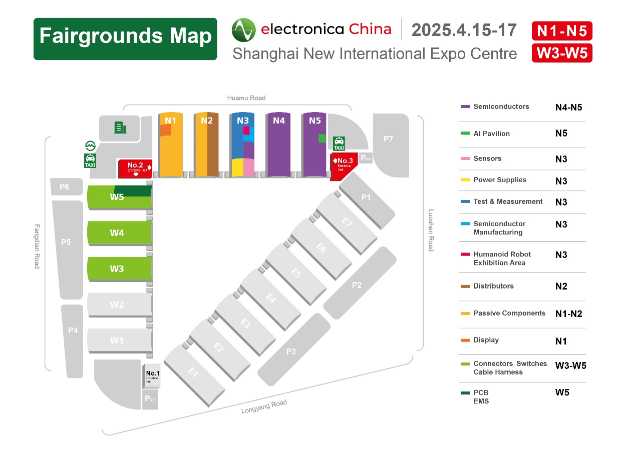
Overview some important exhibition areas
Semiconductors & Sensors
In recent years, the rapid development of the Internet of Things (IoT) industry in China has positioned sensors as one of the core components of the country’s “Strong Foundation Project”. As a result, the market scale and application scenarios for sensors in China have continued to grow. electronica China 2025 will include exhibition areas for semiconductors and sensors, gathering numerous high-quality exhibitors to discuss industry development on-site.
Test and Measurement & Power Supplies
The power supply industry in China has seen rapid growth fueled by international industrial relocation, the ongoing development of China’s information technology, and the continuous advancements in the defense and military sectors. The 2025 exhibition will feature bring together companies to showcase their products and participate in technological discussions in the test and measurement, and power supply exhibition areas.
Connectors, Switches and Cable Harness
In recent years, the connector market has experienced overall growth, fueled by the rapid development of downstream industries such as consumer electronics, new energy vehicles, communications, and industrial control. electronica China 2025 will feature a connector exhibition area, inviting numerous leading exhibitors from the connector industry to showcase their new products.
PCB & EMS
With the maturation of the EMS industry model and ongoing technological advancements and capacity upgrades by companies, the global EMS market is experiencing greater diversity in its downstream customer sectors. At present, EMS is extensively applied across a range of sectors, including consumer electronics, automotive electronics, industrial control electronics, etc. electronica China 2025 will set up PCB and EMS exhibition areas.
Passive Components & Distributors
The development of technologies like 5G communication, artificial intelligence (AI), and the IoT is presenting substantial opportunities for the passive components industry. Additionally, passive components are widely used in such fields as telecommunications, power, automotive electronics, and healthcare, providing substantial growth opportunities for the industry. electronica China 2025 will set up passive components and distributors exhibition areas.
Click to register now: https://ec.global-eservice.com/?lang=en&channel=enmd
Learn more about electronica China: https://www.electronicachina.com.cn/en
The post electronica China 2025: High-quality Chinese and International Companies Gather at this Can’t-miss Electronics Event with 100,000 Square Meters appeared first on ELE Times.
Breaking Boundaries with Photonic Chips and Optical Computing
As traditional semiconductor-based computing approaches its physical and energy efficiency limits, photonic chips and optical computing have emerged as transformative solutions. By harnessing the speed and parallelism of light, these technologies offer significant advantages over conventional electronics in high-performance computing (HPC), artificial intelligence (AI), and data centers. Optical computing has the potential to revolutionize the way information is processed, enabling faster, more energy-efficient computation with lower latency.
The Fundamentals of Photonic ChipsPhotonic chips leverage integrated photonics to manipulate light for computing, communication, and sensing applications. Unlike traditional chips that use electrons as the primary carriers of information, photonic chips use photons, which can travel at the speed of light with minimal energy loss. Key components of photonic chips include:
- Waveguides: Optical channels that guide light through a photonic circuit, analogous to electrical traces in traditional chips.
- Modulators: Convert electrical signals into optical signals by modulating light properties such as intensity or phase.
- Detectors: Convert optical signals back into electrical signals for further processing.
- Resonators and Interferometers: Facilitate advanced signal processing functions such as filtering, multiplexing, and logic operations.
- Photonic Crystals: Control the flow of light by creating periodic dielectric structures, enhancing optical confinement and manipulation.
Optical computing aims to replace or supplement electronic computation with light-based logic operations. This transition offers several key advantages:
- Unparalleled Speed: Photons travel at the speed of light, reducing signal delay and increasing processing throughput.
- Low Energy Consumption: Unlike electrical circuits that suffer from resistive heating, photonic systems dissipate minimal heat, enhancing energy efficiency.
- Massive Parallelism: Optical systems can process multiple data streams simultaneously, significantly improving computational throughput.
- Reduced Signal Crosstalk: Optical signals do not experience the same interference as electrical signals, reducing errors and noise in computation.
Silicon photonics integrates optical components onto a silicon platform, enabling compatibility with existing semiconductor fabrication techniques. Key innovations in silicon photonics include:
- On-chip Optical Interconnects: Replace traditional copper interconnects with optical waveguides to reduce power consumption and signal delay.
- Optical RAM and Memory: Photonic memory elements store and retrieve data using light, enhancing data transfer speeds.
- Electro-Optical Modulators: Convert electronic signals to optical signals efficiently, allowing seamless integration into existing computing architectures.
Optical computing relies on photonic logic gates to perform fundamental computations. These gates operate using:
- Nonlinear Optical Effects: Enable all-optical switching without electronic intermediaries.
- Mach-Zehnder Interferometers (MZI): Implement XOR, AND, and OR logic functions using light phase interference.
- Optical Bistability: Maintains state information in optical latches, paving the way for optical flip-flops and memory elements.
With the growing demand for AI processing, photonic neural networks offer an alternative to traditional GPUs and TPUs. Optical deep learning accelerators employ:
- Matrix Multiplication with Light: Perform multiply-accumulate operations at light speed using photonic interference.
- Optical Tensor Processing Units (TPUs): Enhance AI inference by leveraging photonic components for ultra-fast computation.
- Wavelength-Division Multiplexing (WDM): Enables parallel processing by encoding multiple data streams onto different wavelengths of light.
Quantum computing benefits immensely from photonics due to the inherent properties of quantum light. Advancements in quantum photonic processors include:
- Single-Photon Sources and Detectors: Essential for quantum information processing and cryptographic applications.
- Quantum Key Distribution (QKD): Enables ultra-secure communication leveraging the principles of quantum entanglement.
- Optical Quantum Logic Gates: Facilitate complex quantum computations with minimal decoherence.
Modern data centers face thermal constraints and power limitations due to electronic interconnects. Photonic interconnects dramatically reduce power consumption and increase bandwidth, making them an ideal solution for high-speed data transmission between servers and storage units.
2. Artificial Intelligence and Machine Learning AccelerationAI workloads rely on extensive matrix operations, which photonic computing executes at orders of magnitude faster speeds than traditional electronics. Companies like Lightmatter and Lightelligence are pioneering photonic AI accelerators to enhance deep learning performance while reducing energy costs.
3. Telecommunications and Optical NetworksFiber-optic networks already leverage photonics for data transmission, but photonic computing extends these advantages to real-time processing. Photonic switches enable ultra-fast data routing, improving the efficiency of 5G and future 6G networks.
4. Healthcare and BiophotonicsOptical computing is revolutionizing biomedical imaging and diagnostics. Photonic chips enable high-resolution imaging techniques such as optical coherence tomography (OCT) and bio-sensing applications, enhancing early disease detection.
5. Defense and AerospaceThe military and aerospace industries require ultra-fast, secure processing for signal intelligence, radar systems, and cryptographic applications. Optical computing’s speed and resistance to electromagnetic interference make it a critical enabler for next-generation defense systems.
Challenges and Future Roadmap 1. Fabrication Complexity and ScalabilityWhile photonic chips leverage semiconductor manufacturing techniques, integrating large-scale optical circuits remains a challenge. Standardizing fabrication methods and developing CMOS-compatible photonic components are essential for commercial scalability.
2. Hybrid Photonic-Electronic ArchitecturesDespite the advantages of photonic computing, hybrid architectures that integrate both electronic and optical components are likely to dominate in the near term. Developing efficient electro-optic interfaces remains a key research focus.
3. Software and Algorithm DevelopmentCurrent software is optimized for electronic computation, requiring a shift in programming paradigms for photonic systems. Developing photonic-aware compilers and simulation tools will accelerate adoption.
4. Energy Efficiency and Power ConsumptionWhile photonic computing reduces heat dissipation, the challenge lies in optimizing light generation and detection components to minimize power consumption further.
Conclusion: The Dawn of the Photonic Computing EraPhotonic chips and optical computing represent a paradigm shift in computation, offering unparalleled speed, efficiency, and scalability. As silicon photonics, quantum optics, and neuromorphic photonic computing continue to advance, the technology is poised to revolutionize AI, data centers, telecommunications, and beyond. Overcoming fabrication, software, and integration challenges will be crucial for realizing the full potential of photonic computing, marking the beginning of a new era in information processing.
The post Breaking Boundaries with Photonic Chips and Optical Computing appeared first on ELE Times.
Enhancing Wireless Communication with AI-Optimized RF Systems
The integration of Artificial Intelligence (AI) into Radio Frequency (RF) systems marks a paradigm shift in wireless communications. Traditional RF design relies on static, rule-based optimization, whereas AI enables dynamic, data-driven adaptation. With the rise of 5G, mmWave, satellite communications, and radar technologies, AI-driven RF solutions are crucial for maximizing spectral efficiency, improving signal integrity, and reducing energy consumption.
The Urgency for AI in RF Systems: Industry Challenges & Market TrendsThe RF industry is under immense pressure to meet growing demands for higher data rates, better spectral utilization, and reduced latency. One of the key challenges is Dynamic Spectrum Management, where the increasing scarcity of available spectrum forces telecom providers to adopt intelligent allocation mechanisms. AI-powered systems can predict and allocate spectrum dynamically, ensuring optimal utilization and minimizing congestion.
Another significant challenge is Electromagnetic Interference (EMI) Mitigation. As the density of wireless devices grows, the likelihood of interference between different RF signals increases. AI can analyze vast amounts of data in real-time to predict and mitigate EMI, thus improving overall signal integrity.
Power Efficiency is another major concern, especially in battery-operated and energy-constrained applications. AI-driven power control mechanisms in RF front-ends enable systems to dynamically adjust transmission power based on network conditions, leading to significant energy savings. Additionally, Edge Processing Demands are increasing with the advent of autonomous systems that require real-time, AI-driven RF adaptation for high-speed decision-making and low-latency communications.
Advanced AI Techniques in RF System OptimizationIndustry leaders like Qualcomm, Ericsson, and NVIDIA are investing heavily in AI-driven RF innovations. The following AI methodologies are transforming RF architectures:
Reinforcement Learning for Adaptive Spectrum AllocationAI-driven Cognitive Radio Networks (CRNs) leverage Deep Reinforcement Learning (DRL) to optimize spectrum usage dynamically. By continuously learning from environmental conditions and past allocations, DRL can predict interference patterns and proactively assign spectrum in a way that maximizes efficiency. This allows for the intelligent utilization of both sub-6 GHz and mmWave bands, ensuring high data throughput while minimizing collisions and latency.
Deep Neural Networks for RF Signal Classification & Modulation RecognitionTraditional RF signal classification methods struggle in complex, noisy environments. AI-based techniques such as Convolutional Neural Networks (CNNs) and Long Short-Term Memory (LSTMs) networks enhance modulation recognition accuracy, even in fading channels. These deep learning models can also be used for RF fingerprinting, which improves security by uniquely identifying signal sources. Furthermore, AI-based anomaly detection helps identify and counteract jamming or spoofing attempts in critical communication systems.
AI-Driven Beamforming for Massive MIMO SystemsMassive Multiple-Input Multiple-Output (MIMO) is a cornerstone technology for 5G and 6G networks. AI-driven beamforming techniques use deep reinforcement learning to dynamically adjust transmission beams, improving directional accuracy and link reliability. Additionally, unsupervised clustering methods help optimize beam selection by analyzing traffic load variations, ensuring that the best possible configuration is applied in real-time.
Generative Adversarial Networks (GANs) for RF Signal SynthesisGANs are being explored for RF waveform synthesis, where they generate realistic signal patterns that adapt to changing environmental conditions. This capability is particularly beneficial in electronic warfare (EW) applications, where adaptive waveform generation can enhance jamming resilience. GANs are also useful for RF data augmentation, allowing AI models to be trained on synthetic RF datasets when real-world data is scarce.
AI-Enabled Digital Predistortion (DPD) for Power AmplifiersPower amplifiers (PAs) suffer from nonlinearities that introduce spectral regrowth, degrading signal quality. AI-driven Digital Predistortion (DPD) techniques leverage neural network-based PA modeling to compensate for these distortions in real-time. Bayesian optimization is used to fine-tune DPD parameters dynamically, ensuring optimal performance under varying transmission conditions. Additionally, adaptive biasing techniques help improve PA efficiency by adjusting power consumption based on the input signal’s requirements.
Industry-Specific Applications of AI-Optimized RF SystemsThe impact of AI-driven RF innovation extends across multiple high-tech industries:
Telecommunications: AI-Powered 5G & 6G NetworksAI plays a crucial role in optimizing adaptive coding and modulation (ACM) techniques, allowing for dynamic throughput adjustments based on network conditions. Additionally, AI-enhanced network slicing enables operators to allocate bandwidth efficiently, ensuring quality-of-service (QoS) for diverse applications. AI-based predictive analytics also assist in proactive interference management, allowing networks to mitigate potential disruptions before they occur.
Defense & Aerospace: Cognitive RF for Military ApplicationsIn military communications, AI is revolutionizing RF situational awareness, enabling autonomous systems to detect and analyze threats in real-time. AI-driven electronic countermeasures (ECMs) help counteract enemy jamming techniques, ensuring robust and secure battlefield communications. Machine learning algorithms are also being deployed for predictive maintenance of radar and RF systems, reducing operational downtime and enhancing mission readiness.
Automotive & IoT: AI-Driven RF Optimization for V2X CommunicationVehicle-to-everything (V2X) communication requires reliable, low-latency RF links for applications such as autonomous driving and smart traffic management. AI-powered spectrum sharing ensures that vehicular networks can coexist efficiently with other wireless systems. Predictive congestion control algorithms allow urban IoT deployments to adapt to traffic variations dynamically, improving efficiency. Additionally, AI-driven adaptive RF front-end tuning enhances communication reliability in connected vehicles by automatically adjusting antenna parameters based on driving conditions.
Satellite Communications: AI-Enabled Adaptive Link OptimizationSatellite communication systems benefit from AI-driven link adaptation, where AI models adjust signal parameters based on atmospheric conditions such as rain fade and ionospheric disturbances. Machine learning algorithms are also being used for RF interference classification, helping satellite networks distinguish between different types of interference sources. Predictive beam hopping strategies optimize resource allocation in non-geostationary satellite constellations, improving coverage and efficiency.
The Future of AI-Optimized RF: Key Challenges and Technological RoadmapWhile AI is revolutionizing RF systems, several roadblocks must be addressed. One major challenge is computational overhead, as implementing AI at the edge requires energy-efficient neuromorphic computing solutions. The lack of standardization in AI-driven RF methodologies also hinders widespread adoption, necessitating global collaboration to establish common frameworks. Furthermore, security vulnerabilities pose risks, as adversarial attacks on AI models can compromise RF system integrity.
Future InnovationsOne promising area is Quantum Machine Learning for RF Signal Processing, which could enable ultra-low-latency decision-making in complex RF environments. Another key advancement is Federated Learning for Secure Distributed RF Intelligence, allowing multiple RF systems to share AI models while preserving data privacy. Additionally, AI-Optimized RF ASICs & Chipsets are expected to revolutionize real-time signal processing by embedding AI functionalities directly into hardware.
ConclusionAI-driven RF optimization is at the forefront of wireless communication evolution, offering unparalleled efficiency, adaptability, and intelligence. Industry pioneers are integrating AI into RF design to enhance spectrum utilization, interference mitigation, and power efficiency. As AI algorithms and RF hardware continue to co-evolve, the fusion of these technologies will redefine the future of telecommunications, defense, IoT, and satellite communications.
The post Enhancing Wireless Communication with AI-Optimized RF Systems appeared first on ELE Times.
STM32CubeProgrammer 2.18: Improving the “flow” in “workflow”
Author: STMicroelectronics
STM32CubeProgrammer 2.18 brings new features to improve our developers’ experience. For instance, as we close 2024, flashing and debugging STM32 microcontrollers is more straightforward and intuitive. For instance, the new software leverages STM32 security firmware update (root security system extension binaries), helps change multiple option bytes more efficiently through a synthetic view, and port user configuration settings more easily. It is, therefore, the most user-friendly version yet, as it aims to make development on STM32 feel less like work and more like flow.
What’s new in STM32CubeProgrammer 2.18? New MCU SupportWhile nearly every version of STM32CubeProgrammer comes with new MCU support, 2.18 is particularly noteworthy for the number of added devices. Users can now work with the STM32WL3 announced just a few weeks ago, the STM32N6 launched a few days ago, the new STM32C0 devices with 64 KB and 256 KB of flash.
STM32CubeProgrammer also brings additional feature support for the STM32H7R3/7S3/7R7/7S7, all STM32 MPUs, and the STM32U5. For instance, the STM32H7R/S MCUs can now perform Secure Firmware Installation, while the STM32MP25 gets a GUI to manage PMIC registers and export settings to a binary file, which makes porting them to another project a breeze. And the STM32U5 can now restore its option byte configuration to factory settings if developers make an error that gets them stuck.
New improvements to the user experienceST also continues to increase the number of supported features when using the SEGGER J-Link probe and flasher. In version 2.18, STM32CubeProgrammer adds the ability to securely install the Bluetooth stack on an STM32WB via a J-Link probe. Hence, developers can use their SEGGER tool for more use cases, making these features more widespread.
We are also introducing new improvements to the user experience, such as a project mode that allows users to save and restore configuration and connection settings, option byte values, firmware lists, external flash loaders, security firmware updates (root security system extension binaries), stack install settings for the STM32WB, and automatic mode parameters. In a nutshell, we want developers to collaborate more efficiently by importing and exporting major project elements so they can focus on their code rather than ticking boxes and applying the same settings repeatedly.
STM32CubeProgrammer 2.18 also adds a new synthetic option byte view to see and edit multiple option bytes on a single row instead of having to scroll through detailed lists. For expert users who know exactly what they want to do, this synthetic view makes changing an option byte a lot quicker. Finally, to facilitate updates to RSSe binaries, STM32HSM-V2 personalization files, and option bytes templates, these elements are now delivered separately in the X-CUBE-RSSe expansion package supported by both STM32CubeProgrammer and Trusted Package Creator tools. Consequently, these elements are no longer part of the lastest version of CubeProgrammer and should be downloaded separately.
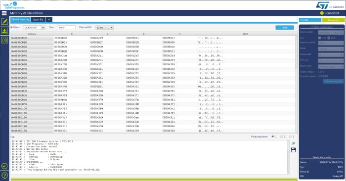
What is STM32CubeProgrammer? An STM32 flasher and debuggerAt its core, STM32CubeProgrammer helps debug and flash STM32 microcontrollers. As a result, it includes features that optimize these two processes. For instance, version 2.6 introduced the ability to dump the entire register map and edit any register on the fly. Previously, changing a register’s value meant changing the source code, recompiling it, and flashing the firmware. Testing new parameters or determining if a value is causing a bug is much simpler today. Similarly, engineers can use STM32CubeProgrammer to flash all external memories simultaneously. Traditionally, flashing the external embedded storage and an SD card demanded developers launch each process separately. STM32CubeProgrammer can do it in one step.
Another challenge for developers is parsing the massive amount of information passing through STM32CubeProgrammer. Anyone who flashes firmware knows how difficult it is to track all logs. Hence, we brought custom traces that allow developers to assign a color to a particular function. It ensures developers can rapidly distinguish a specific output from the rest of the log. Debugging thus becomes a lot more straightforward and intuitive. Additionally, it can help developers coordinate their color scheme with STM32CubeIDE, another member of our unique ecosystem designed to empower creators.
 STM32CubeProgrammer
What are some of its key features?
New MCU support
STM32CubeProgrammer
What are some of its key features?
New MCU support
Most new versions of STM32CubeProgrammer support a slew of new MCUs. For instance, version 2.16 brought compatibility with the 256 KB version of the STM32U0s. The device was the new ultra-low power flagship model for entry-level applications thanks to a static power consumption of only 16 nA in standby. STM32CubeProgrammer 2.16 also brought support for the 512 KB version of the STM32H5, and the STM32H7R and STM32H7S, which come with less Flash so integrators that must use external memory anyway can reduce their costs. Put simply, ST strives to update STM32CubeProgrammer as rapidly as possible to ensure our community can take advantage of our newest platforms rapidly and efficiently.
SEGGER J-Link probe supportTo help developers optimize workflow, we’ve worked with SEGGER to support the J-Link probe fully. This means that the hardware flasher has access to features that were previously only available on an ST-LINK module. For instance, the SEGGER system can program internal and external memory or tweak the read protection level (RDP). Furthermore, using the J-Link with STM32CubeProgrammer means developers can view and modify registers. And since version 2.17, we added the ability to generate serial numbers and automatically increment them within STM32CubeProgrammer, thus hastening the process of flashing multiple STM32s in one batch.
We know that many STM32 customers use the SEGGER probe because it enables them to work with more MCUs, it is fast, or they’ve adopted software by SEGGER. Hence, STM32CubeProgrammer made the J-Link vastly more useful, so developers can do more without leaving the ST software.
Exporting option bytes and editing memory fieldsOther quality-of-life improvements aim to make STM32CubeProgrammer more intuitive. For instance, it is now possible to export an STM32’s option bytes. Very simply, they are a way to store configuration options, such as read-out protection levels, watchdog settings, power modes, and more. The MCU loads them early in the boot process, and they are stored in a specific part of the memory that’s only accessible by debugging tools or the bootloader. By offering the ability to export and import option bytes, STM32CubeProgrammer enables developers to configure MCUs much more easily. Similarly, version 2.17 can now edit memory fields in ASCII to make certain section a lot more readable.
Automating the installation of a Bluetooth LE stackUntil now, developers updating their Bluetooth LE wireless stack had to figure out the address of the first memory block to use, which varied based on the STM32WB and the type of stack used. For instance, installing the basic stack on the STM32WB5x would start at address 0x080D1000, whereas a full stack on the same device would start at 0x080C7000, and the same package starts at 0x0805A000 on the STM32WB3x with 512 KB of memory. Developers often had to find the start address in STM32CubeWB/Projects/STM32WB_Copro_Wireless_Binaries. The new version of STM32CubeProgrammer comes with an algorithm that determines the right start address based on the current wireless stack version, the device, and the stack to install.
A portal to security on STM32Readers of the ST Blog know STM32CubeProgrammer as a central piece of the security solutions present in the STM32Cube Ecosystem. The utility comes with Trusted Package Creator, which enables developers to upload an OEM key to a hardware secure module and to encrypt their firmware using this same key. OEMs then use STM32CubeProgrammer to securely install the firmware onto the STM32 SFI microcontroller. Developers can even use an I2C or SPI interface, which gives them greater flexibility. Additionally, the STM32H735, STM32H7B, STM32L5, STM32U5, and STM32H5 also support external secure firmware install (SFIx), meaning that OEMs can flash the encrypted binary on memory modules outside the microcontroller.
Secure ManagerSecure Manager is officially supported since STM32CubeProgrammer 2.14 and STM32CubeMX 1.13. Currently, the feature is exclusive to our new high-performance MCU, the STM32H573, which supports a secure ST firmware installation (SSFI) without requiring a hardware secure module (HSM). In a nutshell, it provides a straightforward way to manage the entire security ecosystem on an STM32 MCU thanks to binaries, libraries, code implementations, documentation, and more. Consequently, developers enjoy turnkey solutions in STM32CubeMX while flashing and debugging them with STM32CubeProgrammer. It is thus an example of how STM32H5 hardware and Secure Manager software come together to create something greater than the sum of its parts.
Other security features for the STM32H5STM32CubeProgrammer enables many other security features on the STM32H5. For instance, the MCU now supports secure firmware installation on internal memory (SFI) and an external memory module (SFIx), which allows OEMs to flash encrypted firmware with the help of a hardware secure module (HSM). Similarly, it supports certificate generation on the new MCU when using Trusted Package Creator and an HSM. Finally, the utility adds SFI and SFIx support on STM32U5s with 2 MB and 4 MB of flash.
Making SFI more accessibleSTM32CubeProgrammer
Since version 2.11, STM32CubeProgrammer has received significant improvements to its secure firmware install (SFI) capabilities. For instance, in version 2.15, ST added support for the STM32WBA5. Additionally, we added a graphical user interface highlighting addresses and HSM information. The GUI for Trusted Package Creator also received a new layout under the SFI and SFIx tabs to expose the information needed when setting up a secure firmware install. The Trusted package creator also got a graphical representation of the various option bytes to facilitate their configuration.
Secure secret provisioning for STM32MPxSince 2.12, STM32CubeProgrammer has a new graphical user interface to help developers set up parameters for the secure secret provisioning available on STM32MPx microprocessors. The mechanism has similarities with the secure firmware install available on STM32 microcontrollers. It uses a hardware secure module to store encryption keys and uses secure communication between the flasher and the device. However, the nature of a microprocessor means more parameters to configure. STM32CubeProgrammers’ GUI now exposes those settings previously available in the CLI version of the utility to expedite workflows.
Double authenticationSince version 2.9, the STM32CubeProgrammer supports a double authentication system when provisioning encryption keys via JTAG or a Boot Loader for the Bluetooth stack on the STM32WB. Put simply, the feature enables makers to protect their Bluetooth stack against updates from end-users. Indeed, developers can update the Bluetooth stack with ST’s secure firmware if they know what they are doing. However, a manufacturer may offer a particular environment and, therefore, may wish to protect it. As a result, the double authentication system prevents access to the update mechanism by the end user. ST published the application note AN5185 to offer more details.
PKCS#11 supportSince version 2.9, STM32CubeProgrammer supports PKCS#11 when encrypting firmware for the STM32MP1. The Public-Key Cryptography Standards (PKCS) 11, also called Cryptoki, is a standard that governs cryptographic processes at a low level. It is gaining popularity as APIs help embedded system developers exploit its mechanisms. On an STM32MP1, PKCS#11 allows engineers to segregate the storage of the private key and the encryption process for the secure secret provisioning (SSP).
SSP is the equivalent of a Secure Firmware Install for MPUs. Before sending their code to OEMs, developers encrypt their firmware with a private-public key system with STM32CubeProgrammer. The IP is thus unreadable by third parties. During assembly, OEMs use the provided hardware secure module (HSM) containing a protected encryption key to load the firmware that the MPU will decrypt internally. However, until now, developers encrypting the MPU’s code had access to the private key. The problem is that some organizations must limit access to such critical information. Thanks to the new STM32CubeProgrammer and PKCS#11, the private key remains hidden in an HSM, even during the encryption process by the developers.
Supporting new STM32 MCUs STM32C0, STM32MP25, and STM32WB05/6/7Since version 2.17, STM32CubeProgrammer supports STM32C0s with 128 KB of flash. It also recognizes the STM32MP25, which includes a 1.35-TOPS NPU, and all the STM32WB0s, including the STM32WB05, STM32WB05xN, STM32WB06, and STM32WB07. In the latter case, we brought support only a few weeks after their launch, thus showing that STM32CubeProgrammer keeps up with the latest releases to ensure developers can flash and debug their code on the newest STM32s as soon as possible.
Access to the STM32MP13’s bare metalMicrocontrollers demand real-time operating systems because of their limited resources, and event-driven paradigms often require a high level of determinism when executing tasks. Conversely, microprocessors have a lot more resources and can manage parallel tasks better, so they use a multitasking operating system, like OpenSTLinux, our Embedded Linux distribution. However, many customers familiar with the STM32 MCU world have been asking for a way to run an RTOS on our MPUs as an alternative. In a nutshell, they want to enjoy the familiar ecosystem of an RTOS and the optimizations that come from running bare metal code while enjoying the resources of a microprocessor.
Consequently, we are releasing today STM32CubeMP13, which comes with the tools to run a real-time operating system on our MPU. We go into more detail about what’s in the package in our STM32MP13 blog post. Additionally, to make this initiative possible, ST updated its STM32Cube utilities, such as STM32CubeProgrammer. For instance, we had to ensure that developers could flash the NOR memory. Similarly, STM32CubeProgrammer enables the use of an RTOS on the STM32MP13 by supporting a one-time programmable (OTP) partition.
Traditionally, MPUs can use a bootloader, like U-Boot, to load the Linux kernel securely and efficiently. It thus serves as the ultimate first step in the boot process, which starts by reading the OTP partition. Hence, as developers move from a multitasking OS to an RTOS, it was essential that STM32CubeProgrammer enable them to program the OTP partition to ensure that they could load their operating system. The new STM32CubeProgrammer version also demonstrates how the ST ecosystem works together to release new features.
STM32WB and STM32WBA supportSince version 2.12, STM32CubeProgrammer has brought numerous improvements to the STM32WB series, which is increasingly popular in machine learning applications, as we saw at electronica 2022. Specifically, the ST software brings new graphical tools and an updated wireless stack to assist developers. For instance, the tool has more explicit guidelines when encountering errors, such as when developers try to update a wireless stack with the anti-rollback activated but forget to load the previous stack. Similarly, new messages will ensure users know if a stack version is incompatible with a firmware update. Finally, STM32CubeProgrammer provides new links to download STM32WB patches and get new tips and tricks so developers don’t have to hunt for them.
Similarly, STM32CubeProgrammer supports the new STM32WBA, the first wireless Cortex-M33. Made official a few months ago, the MCU opens the way for a Bluetooth Low Energy 5.3 and SESIP Level 3 certification. The MCU also has a more powerful RF that can reach up to +10 dBm output power to create a more robust signal.
STM32H5 and STM32U5The support for STM32H5 began with STM32CubeProgrammer 2.13, which added compatibility with MCUs, including anything from 128 KB up to 2 MB of flash. Initially, the utility brought security features like debug authentication and authentication key provisioning, which are critical when using the new life management system. The utility also supported key and certificate generation, firmware encryption, and signature. Over time, ST added support for the new STM32U535 and STM32U545 with 512 KB and 4 MB of flash. The MCUs benefit from RDP regression with a password to facilitate developments and SFI secure programming.
Additionally, STM32CubeProgrammer includes an interface for read-out protection (RDP) regression with a password for STM32U5xx. Developers can define a password and move from level 2, which turns off all debug features, to level 1, which protects the flash against certain reading or dumping operations, or to level 0, which has no protections. It will thus make prototyping vastly simpler.
STLINK-V3PWRIn many instances, developers use an STLINK probe with STM32CubeProgrammer to flash or debug their device. Hence, we quickly added support for our latest STLINK-PWR probe, the most extensive source measurement unit and programmer/debugger for STM32 devices. If users want to see energy profiles and visualize the current draw, they must use STM32CubeMonitor-Power. However, STM32CubeProgrammer will serve as an interface for all debug features. It can also work with all the probe’s interfaces, such as SPI, UART, I2C, and CAN.
Script modeThe software includes a command-line interface (CLI) to enable the creation of scripts. Since the script manager is part of the application, it doesn’t depend on the operating system or its shell environment. As a result, scripts are highly sharable. Another advantage is that the script manager can maintain connections to the target. Consequently, STM32CubeProgrammer CLI can keep a connection live throughout a session without reconnecting after every command. It can also handle local variables and even supports arithmetic or logic operations on these variables. Developers can thus create powerful macros to automate complex processes. To make STM32CubeProgrammer CLI even more powerful, the script manager also supports loops and conditional statements.
A unifying experienceSTM32CubeProgrammer aims to unify the user experience. ST brought all the features of utilities like the ST-LINK Utility, DFUs, and others to STM32CubeProgrammer, which became a one-stop shop for developers working on embedded systems. We also designed it to work on all major operating systems and even embedded OpenJDK8-Liberica to facilitate its installation. Consequently, users do not need to install Java themselves and struggle with compatibility issues before experiencing STM32CubeProgrammer.
Qt 6 supportSince STM32CubeProgrammer 2.16, the ST utility uses Qt 6, the framework’s latest version. Consequently, STM32CubeProgrammer no longer runs on Windows 7 and Ubuntu 18.04. However, Qt 6 patches security vulnerabilities, brings bug fixes, and comes with significant quality-of-life improvements.
The post STM32CubeProgrammer 2.18: Improving the “flow” in “workflow” appeared first on ELE Times.
Advanced Packaging Solutions: Pushing the Limits of Semiconductor Performance
As Moore’s Law faces physical limitations, the semiconductor industry is increasingly turning to advanced packaging solutions to sustain performance gains. Traditional monolithic scaling is no longer viable for delivering the power efficiency and computational throughput required by next-generation applications like artificial intelligence (AI), high-performance computing (HPC), 5G, and edge computing. Instead, innovations in heterogeneous integration, 2.5D and 3D packaging, chiplet architectures, and fan-out wafer-level packaging (FOWLP) are redefining performance metrics.
This article provides an in-depth analysis of cutting-edge packaging technologies, their impact on semiconductor performance, and real-world case studies from leading industry players such as Broadcom, Nvidia, and GlobalFoundries.
The Evolution of Advanced Packaging Technologies- 2.5D Integration: The Bridge Between Traditional and 3D Packaging
2.5D integration involves placing multiple semiconductor dies on a silicon interposer, allowing high-speed interconnections. Unlike conventional multi-chip modules (MCMs), 2.5D technology provides lower latency due to short interconnect distances, higher bandwidth through wide bus architectures, and reduced power consumption by eliminating long copper traces. These advantages make it an ideal solution for applications requiring high computational power and data transfer speeds.
Case StudyBroadcom’s 3.5D XDSiP for AI Acceleration Broadcom recently introduced 3.5D Extended Data Scale in Package (XDSiP) technology, enhancing AI chip interconnectivity using TSMC’s advanced packaging techniques. With production shipments expected by 2026, Broadcom aims to support hyperscale cloud providers in meeting AI’s high bandwidth demands by leveraging this innovative packaging solution.
- 3D Stacking: The Revolution in Vertical Integration
Unlike 2.5D, 3D stacking vertically integrates multiple dies using Through-Silicon Vias (TSVs) and wafer-to-wafer bonding. This architecture significantly reduces data transmission delays, lowers power dissipation, and increases computational density. By enabling high-speed data transfer with minimal signal loss, 3D stacking is particularly useful for applications requiring fast processing speeds. Additionally, the smaller form factors allow for more compact semiconductor devices, while improved thermal efficiency is achieved through optimized heat dissipation layers.
Case StudyNvidia’s CoWoS-L in AI Chips Nvidia’s latest AI processor, Blackwell, utilizes Chip-on-Wafer-on-Substrate Large (CoWoS-L) technology, moving beyond traditional CoWoS-S to enhance interconnect performance. This advancement is part of Nvidia’s broader strategy to improve AI workload efficiency and silicon utilization, ensuring faster and more efficient data processing capabilities.
- Chiplet-Based Architectures: The Future of Modular Semiconductor Design
The industry is transitioning toward chiplet architectures, where small, specialized dies are interconnected within a package to increase performance flexibility and yield efficiency. Unlike monolithic designs, chiplets enable heterogeneous integration, allowing processors, memory, and accelerators to coexist within a single package. This approach reduces manufacturing costs by reusing tested chiplets while improving scalability by mixing process nodes within a package. Additionally, smaller die sizes contribute to better yield efficiency, ultimately enhancing semiconductor performance and reliability.
Case StudyAMD’s EPYC and Intel’s Meteor Lake AMD and Intel have embraced chiplet designs to improve scalability in their high-performance processors. AMD’s EPYC server CPUs leverage multiple CCD (Core Complex Die) chiplets, while Intel’s Meteor Lake integrates different chiplets for CPU, GPU, and AI acceleration, demonstrating the advantages of modular semiconductor design.
- Fan-Out Wafer-Level Packaging (FOWLP): Enhancing Thermal and Electrical Performance
FOWLP extends the package beyond the die’s boundaries, increasing I/O density while maintaining a compact footprint. This method eliminates wire bonding, improving electrical and thermal properties. With higher bandwidth compared to traditional wire-bond packaging, FOWLP enhances signal integrity while providing better heat dissipation for high-power applications. Furthermore, reduced parasitic capacitance ensures minimal signal interference, making this packaging technique essential for next-generation semiconductor devices.
Case StudyApple’s A-Series Processors Apple extensively uses FOWLP in its A-series chips, ensuring high-performance computing in iPhones and iPads with minimized power loss and improved thermal control. By integrating this packaging solution, Apple enhances both power efficiency and processing capabilities, delivering seamless user experiences.
Impact of Advanced Packaging on Semiconductor Performance- Performance Gains: Pushing Computational Boundaries
By reducing interconnect lengths and signal latency, advanced packaging significantly enhances processing speeds for AI and HPC applications. Improved memory bandwidth allows for faster data transfer, benefiting workloads such as AI model training and deep learning inference. Additionally, data center efficiency is greatly improved as power-hungry interconnect bottlenecks are minimized, ensuring higher computational throughput.
- Power Efficiency: Addressing Thermal Constraints
Advanced packaging solutions lower power consumption by optimizing shorter interconnect paths that reduce energy dissipation. Better thermal management is achieved using advanced cooling layers, preventing overheating issues in high-performance applications. The integration of energy-efficient AI accelerators, such as low-power chiplets, further enhances power efficiency, ensuring sustainable semiconductor performance.
- Miniaturization and Integration: The Path to More Compact Devices
With increasing demand for smaller form factors, advanced packaging enables higher transistor densities, improving device functionality. The integration of specialized components, such as RF, memory, and AI accelerators, allows for more efficient processing while maintaining compact device sizes. Heterogeneous system architectures facilitate multi-functional capabilities, paving the way for highly sophisticated semiconductor solutions.
Challenges in Advanced Packaging Adoption- Manufacturing Complexity
The fabrication of interposers and TSVs in advanced packaging incurs high costs due to precision alignment requirements. Yield challenges arise as the complexity of packaging increases, necessitating stringent quality control measures to ensure production efficiency.
- Thermal Management Issues
As power density increases, overheating becomes a major challenge in advanced packaging. To counter this, new cooling solutions such as liquid and vapor chamber technologies are being explored to enhance heat dissipation and ensure thermal stability in high-performance devices.
- Design & Validation Bottlenecks
With the rise of chiplet-based designs, EDA tools need advancements to model complex architectures accurately. Testing complexity also increases due to heterogeneous integration, requiring innovative validation techniques to streamline semiconductor development.
Future Trends in Semiconductor Packaging- Heterogeneous Integration at Scale
The future of semiconductor packaging lies in combining logic, memory, and RF components within a unified package. This integration will pave the way for neuromorphic and quantum computing applications, unlocking new possibilities in computational efficiency.
- Advanced Materials for Packaging
High-performance substrates, such as glass interposers, are gaining traction for improving signal integrity. Additionally, the development of low-k dielectrics is expected to reduce capacitance losses, further enhancing semiconductor performance.
- Standardization of Chiplet Interconnects
Industry efforts like UCIe (Universal Chiplet Interconnect Express) aim to create cross-compatible chiplet ecosystems, allowing seamless integration of different semiconductor components.
- AI-Driven Automation in Packaging Design
Generative AI algorithms are optimizing power, performance, and area (PPA) trade-offs, accelerating semiconductor design processes. AI-enabled defect detection and yield improvement strategies are also becoming integral to advanced packaging manufacturing.
Conclusion: The Road Ahead for Semiconductor Performance EnhancementAdvanced packaging is reshaping the future of semiconductor design, driving performance improvements across AI, HPC, and mobile computing. As the industry continues to innovate, overcoming challenges in manufacturing, thermal management, and validation will be crucial in sustaining growth. The next decade will witness a convergence of materials science, AI-driven automation, and heterogeneous integration, defining a new era of semiconductor technology.
The post Advanced Packaging Solutions: Pushing the Limits of Semiconductor Performance appeared first on ELE Times.
Steel Soldering: Definition, Process, Working, Uses & Advantages
Steel soldering is a metal-joining process used to bond steel components by melting a filler metal with a lower melting point than the steel itself. Unlike welding, which fuses the base metals together, or brazing, which uses higher temperatures, soldering operates at relatively low temperatures (typically below 450°C or 840°F). This makes it suitable for delicate applications where excessive heat could damage the materials.
Soldering steel is more challenging than soldering other metals like copper or brass due to steel’s oxidation properties and lower thermal conductivity. To ensure a strong joint, fluxes and specialized soldering materials, such as tin-lead or silver-based alloys, are commonly used.
How Steel Soldering WorksSteel soldering follows a systematic approach that involves surface preparation, application of heat, and bonding with the help of solder and flux. The key principle behind the process is capillary action, where the molten solder flows into the microscopic gaps between metal surfaces, creating a strong mechanical and electrical bond.
The success of steel soldering depends on various factors, including the type of flux, the choice of solder alloy, and the precision of temperature control. Proper surface cleaning and oxide removal are crucial to achieving a reliable bond, as steel tends to develop an oxide layer that inhibits solder adhesion.
Steel Soldering ProcessThe steel soldering process consists of several essential steps. First, surface preparation is crucial. The steel surfaces must be cleaned thoroughly using sandpaper, steel wool, or chemical cleaners to remove dirt, grease, and oxidation. Once cleaned, an appropriate flux, such as zinc chloride or rosin-based flux, is applied to prevent oxidation and promote solder flow.
Next, selecting the right solder and flux is important. Lead-free solder alloys such as silver-based or tin-copper alloys are recommended for environmental safety. The flux should be compatible with the solder alloy to ensure proper wetting and adhesion.
The heating process follows, where a soldering iron, torch, or induction heating is used to bring the steel to the required temperature. Uniform heating is necessary to avoid weak joints and improper solder flow. Once the joint reaches the solder’s melting point, the solder wire or paste is introduced. The molten solder then flows into the joint through capillary action.
After soldering, the joint should be allowed to cool naturally without disturbance to prevent cracking. Once cooled, residual flux and oxidation are removed using warm water or specialized cleaning agents to ensure long-term durability.
Steel Soldering Uses & ApplicationsSteel soldering finds applications in a wide range of industries due to its ability to create strong, reliable joints at low temperatures. In the electronics and electrical industry, it is used in circuit boards, connectors, and electrical components where steel parts need reliable connections. It is also utilized for shielding applications for electromagnetic interference (EMI) protection.
In the automotive and aerospace industries, steel soldering is employed in small, heat-sensitive components, such as sensors and electrical connectors. Aerospace applications require precise soldering of critical parts to maintain structural integrity.
The HVAC systems and plumbing industries also benefit from steel soldering, particularly in joining refrigeration coils, pipe fittings, and heat exchangers. This method provides leak-proof and corrosion-resistant joints essential for efficient system performance.
Additionally, steel soldering is widely used in jewellery making and artistic metalwork. It allows artisans to create custom metal pieces, repair jewellery, and design decorative steel structures while maintaining an aesthetically pleasing finish. The medical industry also utilizes steel soldering in the manufacturing of surgical instruments and medical devices, ensuring precise and biocompatible metal bonding.
Steel Soldering AdvantagesSteel soldering offers several advantages over other metal joining methods, making it an ideal choice for specific applications. One major advantage is its low heat requirement. Unlike welding, which involves high temperatures that can cause warping or damage, soldering operates at much lower temperatures, preserving the integrity of delicate components.
Another significant benefit is its versatility. Steel soldering can be used on thin or intricate steel components without compromising their structural integrity. The process creates strong and reliable bonds that are resistant to corrosion, ensuring long-term durability.
Cost-effectiveness is another advantage, as soldering requires minimal equipment and energy compared to welding and brazing. This makes it an economical choice for small-scale manufacturing and repairs. Moreover, soldering is relatively easy to learn and perform, requiring minimal training and no specialized machinery, making it accessible to both professionals and hobbyists.
A notable safety advantage is that soldering does not require specialized protective equipment. Unlike welding, which necessitates protective gear against UV radiation and fumes, soldering is a safer process with fewer health hazards.
Steel Soldering DisadvantagesDespite its benefits, steel soldering has certain limitations. One major drawback is that soldered joints are not as strong as welded joints, making them unsuitable for high-load applications. Additionally, soldered joints have limited heat resistance and may fail under high temperatures, restricting their use in environments where elevated temperatures are a concern.
Another challenge is oxidation. Steel tends to form an oxide layer quickly, which can hinder solder adhesion. This requires the use of aggressive fluxes or pre-cleaning treatments to ensure a strong bond. Environmental concerns also arise with traditional lead-based solder, as it poses health and environmental risks, leading to a shift toward lead-free alternatives.
Lastly, some fluxes used in the soldering process leave corrosive residues that must be thoroughly cleaned to prevent long-term damage to the joint. Proper cleaning procedures are necessary to maintain joint integrity and prevent issues such as corrosion or weak bonding over time.
ConclusionSteel soldering is a valuable technique for low-temperature metal bonding, offering numerous advantages in electronics, automotive, HVAC, and medical applications. While it has certain limitations, proper material selection, surface preparation, and soldering techniques can help achieve strong and reliable bonds. As advancements in soldering technology continue, steel soldering is becoming even more efficient and environmentally friendly, making it a crucial method in modern manufacturing and repair industries.
The post Steel Soldering: Definition, Process, Working, Uses & Advantages appeared first on ELE Times.
Understanding Metal Soldering: Definition, Process, Working, Uses & Advantages
Metal soldering is a process used to join two or more metal surfaces by melting a filler metal, known as solder, without melting the base metals. The solder, which has a lower melting point than the metals being joined, flows into the joint through capillary action and solidifies upon cooling, creating a strong bond. Unlike welding, where the base metals are melted, soldering relies on a low-heat process, making it ideal for delicate components and applications where excessive heat can cause damage.
Soldering is widely used in electronics, plumbing, automotive repairs, jewellery making, and industrial metalworking. It is favoured for its precision, conductivity, and versatility, allowing for secure, reliable connections between different metal components. With recent advancements, lead-free solder alloys and improved flux formulations have made soldering safer and more environmentally friendly.
How Metal Soldering Works?Metal soldering works by applying heat to a joint and introducing a solder alloy, which melts and adheres to the metal surfaces, forming a secure connection. The process involves several key elements, including a heat source, such as a soldering iron, torch, or induction heater, flux to clean and prepare the metal surface, and solder wire or paste to create the bond.
The key principle behind soldering is capillary action, where the molten solder flows into the tiny gaps between metal surfaces. This ensures that the joint is uniform, strong, and conductive. Proper temperature control is crucial because overheating can damage components or weaken the bond, while insufficient heat may result in a poor connection.
Different types of soldering are used based on the temperature and strength required, including soft soldering, hard soldering (silver soldering), and brazing. Each method serves different industrial needs, ranging from electronic circuit board assembly to high-strength mechanical joints in automotive and aerospace applications.
Metal Soldering ProcessThe metal soldering process follows a step-by-step approach to ensure a strong, reliable joint.
1. Surface PreparationBefore soldering, the metal surfaces must be thoroughly cleaned to remove any oxidation, oil, or dirt that could interfere with solder adhesion. This is done using abrasive pads, sandpaper, chemical cleaners, or specialized fluxes that dissolve impurities. Flux is particularly important because it prevents oxidation during the heating process, ensuring a smooth flow of solder.
2. Heating the JointThe joint is then heated using a soldering iron, gas torch, or induction heater, depending on the type of soldering being performed. The temperature must be carefully controlled to prevent excessive heating, which can weaken the joint or damage heat-sensitive components. The goal is to heat the metal surfaces just enough to allow the solder to flow and bond properly.
3. Applying the SolderOnce the joint reaches the correct temperature, solder wire, paste, or pre-formed solder pieces are introduced. The solder melts upon contact with the heated surface and flows into the joint through capillary action, ensuring an even distribution. The use of flux helps the solder adhere properly by removing any remaining oxides and improving wetting.
4. Cooling and SolidificationAfter the solder has flowed into the joint, the heat source is removed, and the connection is allowed to cool naturally. Rapid cooling should be avoided, as it can create thermal stress and weak bonds. The solder solidifies as it cools, forming a strong electrical and mechanical connection.
5. Cleaning the JointOnce cooled, the joint is inspected for smoothness, strength, and uniformity. Any excess flux residue is cleaned using isopropyl alcohol (IPA) or water, as leftover flux can cause corrosion over time. In electronics soldering, a multimeter may be used to check electrical continuity and ensure a reliable connection.
Types of Metal Soldering 1. Soft Soldering (Low-Temperature Soldering)Soft soldering is the most commonly used method, particularly in electronics and plumbing. It uses a low-melting-point solder alloy, typically containing tin and lead (Sn-Pb) or a lead-free alternative (Sn-Ag-Cu). The temperatures in soft soldering typically range from 180°C to 300°C. Since soft soldering does not require extremely high temperatures, it is ideal for delicate applications such as circuit board assembly and small metal components.
2. Hard Soldering (Silver Soldering)Hard soldering, also known as silver soldering, uses a higher-melting-point solder, often containing silver or other strong alloys. This technique requires temperatures between 450°C and 800°C and is commonly used in jewellery making, refrigeration systems, and aerospace applications. Hard soldering produces stronger and more heat-resistant joints than soft soldering, making it suitable for high-stress environments.
3. Brazing (High-Temperature Soldering)Brazing is similar to soldering but uses a filler metal with a melting point above 800°C. The process involves heating the metal surfaces and allowing brass or bronze-based solder to flow into the joint. Brazing is widely used in automotive manufacturing, HVAC systems, and heavy-duty industrial applications where high-strength, heat-resistant joints are required.
Uses & Applications of Metal Soldering 1. Electronics & PCB ManufacturingSoldering is an essential process in electronics assembly, used to join circuit board components, connectors, and microchips. It ensures electrical conductivity and mechanical stability, making it crucial for manufacturing computers, smartphones, and consumer electronics. With the rise of lead-free soldering due to environmental regulations (RoHS compliance), manufacturers now use tin-silver-copper (SAC) alloys for improved safety and durability.
2. Plumbing & Pipe FittingsSoft soldering is widely used in plumbing systems to create leak-proof seals in copper pipes and water lines. It provides durable, corrosion-resistant joints that withstand water pressure and temperature fluctuations.
3. Automotive & Aerospace IndustriesSoldering is used in wiring, sensors, and heat-sensitive components in automotive and aerospace engineering. Hard soldering and brazing are preferred for fuel lines, air-conditioning systems, and exhaust components, ensuring high-strength, heat-resistant bonds.
4. Jewellery & MetalworkIn the jewellery industry, silver soldering is used to join gold, silver, and platinum pieces with minimal heat damage. It ensures seamless, durable joints without affecting intricate designs.
Advantages of Metal SolderingOne of the key benefits of metal soldering is its low-temperature operation, which prevents the base metals from melting or warping. It also allows for precise, clean joints, making it ideal for electronics and fine metalwork. The process provides strong, conductive bonds, ensuring reliable electrical connections in circuit boards. Additionally, soldering is cost-effective, energy-efficient, and versatile, working with a wide range of metals.
Disadvantages of Metal SolderingDespite its benefits, soldering has some limitations. It produces joints that are not as strong as welded connections, making it unsuitable for high-load applications. Heat-sensitive materials can be damaged if temperature control is poor, and flux residues can lead to corrosion if not cleaned properly. Additionally, soft soldering has temperature limitations, as joints may fail under extreme heat or stress.
ConclusionMetal soldering remains a critical process in modern manufacturing and repair work, offering a precise, low-temperature, and cost-effective method for joining metals. With the rise of lead-free alloys, automation, and advanced flux formulations, soldering continues to evolve, making it safer and more efficient. Whether in electronics, plumbing, automotive, or jewellery making, soldering provides reliable, durable connections that drive innovation in multiple industries.
The post Understanding Metal Soldering: Definition, Process, Working, Uses & Advantages appeared first on ELE Times.
Stealth Technology: Definition, Types, Working & Applications
Stealth technology, also known as low observable technology, is a collection of advanced techniques designed to reduce the visibility of military vehicles, aircraft, ships, and missiles to enemy detection systems. These systems include radar, infrared sensors, sonar, and electromagnetic surveillance tools. The primary objective of stealth technology is to increase the survivability of military assets by making them harder to detect, track, and target.
The concept of stealth technology is not new, but it has evolved significantly with advancements in material science, aerodynamics, and electronic warfare. Early efforts in stealth technology focused on reducing the radar cross-section (RCS) of aircraft through unique shaping techniques. Over time, innovations in radar-absorbing materials (RAM), infrared suppression systems, and acoustic noise reduction have led to highly sophisticated stealth platforms. Today, stealth technology is a crucial element in modern warfare, providing a significant strategic advantage in aerial, naval, and ground operations.
Types of Stealth TechnologyStealth technology can be classified into several types based on the method used to reduce detectability. Each type focuses on minimizing a specific form of detection, ensuring that military assets remain hidden from enemy sensors.
Radar Stealth (Low Radar Cross Section – RCS)
Radar stealth technology primarily aims to minimize the amount of radar waves reflected back to enemy detection systems. The radar cross-section (RCS) of an object is a measure of how much radar energy it reflects, and stealth technology works by reducing this reflection. One of the key techniques used in radar stealth is designing aircraft and naval vessels with faceted surfaces or smooth curves that scatter incoming radar waves rather than reflecting them directly back to the source.
Additionally, specialized radar-absorbing materials (RAM) are used to coat stealth vehicles. These materials absorb a significant portion of the radar energy, converting it into heat rather than allowing it to be reflected. Aircraft like the F-22 Raptor and B-2 Spirit bomber use a combination of these techniques to achieve low radar detectability.
Infrared (IR) Stealth
Infrared stealth focuses on reducing an object’s heat signature to avoid detection by thermal imaging systems. Military aircraft, ships, and land vehicles generate significant heat due to engine operations, friction with the air, and exhaust emissions. Advanced stealth technology incorporates several techniques to minimize this infrared signature.
One method involves using heat-dissipating exhaust systems that spread the hot gases over a larger area, thereby lowering their temperature before they escape into the atmosphere. Additionally, stealth aircraft often use low-emissivity materials on their surfaces to prevent excessive heat buildup. These techniques make it harder for enemy infrared sensors to detect and lock onto stealth platforms, increasing their survivability in combat zones.
Acoustic Stealth
Acoustic stealth technology is essential for submarines and naval vessels, where sound waves are used to detect objects underwater. Noise generated by propellers, engines, and onboard systems can be detected by sonar, making it crucial to minimize acoustic emissions.
To achieve acoustic stealth, submarines and stealth ships use quiet propulsion systems that reduce cavitation—the formation of air bubbles around propeller blades that create noise. Additionally, sound-absorbing materials are used to coat the hulls of submarines, dampening vibrations and reducing noise transmission. These techniques allow stealth submarines, such as the Virginia-class and Scorpène-class, to operate undetected in enemy waters.
Visual Stealth
Visual stealth technology aims to reduce the visibility of military assets using advanced camouflage techniques. Traditional methods involve painting vehicles with camouflage patterns that help them blend into their surroundings. However, modern stealth technology has taken this a step further with the development of electrochromic materials and adaptive coatings that can change colour based on environmental conditions.
Some experimental visual stealth systems use metamaterials and active cloaking technologies that manipulate light waves, making an object appear nearly invisible to the naked eye. While full optical invisibility remains a challenge, ongoing research continues to push the boundaries of visual stealth.
Electromagnetic Stealth
In addition to reducing radar and infrared signatures, stealth technology also minimizes electromagnetic emissions from military platforms. Electronic devices, including communication and navigation systems, emit detectable signals that can be intercepted by enemy intelligence operations. To prevent detection, stealth aircraft, and naval vessels use electromagnetic shielding to contain these emissions.
Moreover, emission control (EMCON) procedures are employed to limit unnecessary electronic transmissions, reducing the risk of detection by enemy surveillance systems. By managing their electromagnetic footprint, stealth platforms can operate more securely in hostile environments.
How Does Stealth Technology Work?Stealth technology works by integrating multiple techniques to reduce the chances of detection across various sensory domains. One of the most important aspects is the reduction of radar cross-section (RCS), which is achieved through specialized aircraft shaping and radar-absorbing coatings. By ensuring that radar waves are either absorbed or deflected away from enemy sensors, stealth aircraft like the F-35 Lightning II can remain undetected for longer durations.
Infrared suppression techniques help control heat emissions, making it difficult for heat-seeking missiles to lock onto stealth assets. Noise reduction strategies ensure that submarines and naval vessels can move through water without alerting enemy sonar systems. Additionally, electromagnetic stealth reduces radio frequency emissions, preventing enemy forces from pinpointing the location of stealth aircraft, ships, or drones.
Applications of Stealth TechnologyStealth technology has a wide range of applications in modern military operations.
Stealth Aircraft
Stealth aircraft play a crucial role in modern aerial warfare by conducting deep penetration strikes, surveillance missions, and air superiority operations. Notable examples include the F-22 Raptor, a highly maneuverable stealth fighter designed for air dominance, and the B-2 Spirit, a stealth bomber capable of delivering nuclear and conventional payloads with minimal risk of detection.
Stealth Naval Vessels
Naval stealth technology enhances the survivability of warships by reducing their radar and acoustic signatures. The USS Zumwalt (DDG-1000) is an advanced destroyer with a stealthy design that minimizes its radar cross-section. Similarly, the Type 055 destroyer, developed by China, incorporates stealth shaping to improve operational effectiveness in naval engagements.
Stealth Submarines
Submarines rely heavily on stealth to avoid detection while patrolling enemy waters. The Virginia-class submarines used by the U.S. Navy feature anechoic coatings and quiet propulsion systems that make them nearly undetectable by sonar. The Scorpène-class submarines, developed by France, are also known for their stealth capabilities and operational flexibility.
Stealth Missiles and Drones
Stealth technology is increasingly being integrated into unmanned systems and precision-guided missiles. The BGM-109 Tomahawk cruise missile is designed to have a low radar cross-section, allowing it to evade enemy air defenses. Similarly, the RQ-170 Sentinel is a stealth reconnaissance drone used for intelligence-gathering missions.
Advantages of Stealth TechnologyStealth technology provides several advantages in military operations. By reducing an asset’s detectability, it enhances survivability, allowing forces to carry out missions with lower risk. Stealth platforms also improve operational effectiveness by enabling surprise attacks and reconnaissance missions without alerting enemy defenses. Additionally, stealth technology provides a strategic advantage by forcing adversaries to invest in more advanced detection and countermeasure systems.
ConclusionStealth technology has revolutionized modern warfare by enabling military forces to operate with greater security and effectiveness. From radar-absorbing materials to infrared suppression and electromagnetic shielding, stealth innovations continue to evolve, shaping the future of aerial, naval, and ground combat. As research advances, stealth technology may find applications beyond the military, influencing commercial aviation and security technologies in the coming decades.
The post Stealth Technology: Definition, Types, Working & Applications appeared first on ELE Times.
Сторінки

