
Microelectronics world news
GaN vs SiC: A look at two popular WBG semiconductors in power

Wide bandgap semiconductors have taken both power electronics and high frequency circuits by storm, replacing so many applications that were previously dominated by silicon-based devices, e.g., LDMOS HPAs in base stations, IGBTs in high voltage DC/DC conversion etc. Specifically within power electronics, it is no secret that certain applications are demanding power dense solutions that operate at high switching frequencies to minimize switching losses. From traction inverters, onboard chargers, and high voltage DC-DC converters in EVs to uninterruptible power supplies (UPSs) and solar power converters in industrial/commercial applications; WBG semiconductors have carved out an extensive niche for many next generation electronics.
The SiC substrate has established itself for EV and some industrial applications. However, a bit more recently GaN has surfaced as a strong option for many overlapping applications. Understanding the major differences between these substrates in the context of high power circuits and their respective manufacturing considerations might shed light on the future of these two popular compound semiconductors.
WBG benefitsWBG materials are inherently able to operate at higher switching frequencies and with higher electric fields than the conventional Si substrate. When a semiconductor is heated up, its resistance tends to go down due to thermally excited carriers that are more abundant at higher temperatures, causing conduction. Higher bandgap semiconductors will require higher temperatures (more energy) to excite electrons across the bandgap from the valence band to the conduction band. This translates directly to more power handling capabilities and higher device efficiencies.
This can be seen in Table 1 where SiC and GaN exhibit much higher breakdown electric field, electron mobility, saturation velocity, and thermal conductivity than Si—all factors that enhance switching frequency and power density. However, high switching frequencies will lead to more losses and a lower efficiency FET, this is where optimizing the power device figure of merit (FoM) [Rds(on) x Qg], or optimizing the channel resistance and gate charge for lower conduction and switching losses, is critical.
|
Properties |
Si |
SiC |
GaN |
|
Band Gap (eV) |
1.12 |
3.3 |
3.44 |
|
Critical Breakdown Electric Field (V/cm) x106 |
0.3 |
2 to 4 |
3.3 |
|
Electron Mobility (cm2/Vs) |
1000 to 1400 |
650 |
1500 to 2000 |
|
Saturation Velocity (cm/s) x107 |
1 |
2 |
2.2 |
|
Thermal Conductivity (W/cm K) |
1.5 |
4.9 |
1.3 to 2.2 |
Table 1 Properties of Si, SiC, and GaN.
Generally, GaN FETs max out at around 650-V with power applications around 10 kW while 750-V and 1200-V SiC FETs are not unusual and applications can range from 1 kW up to the megawatts (Figure 1). SiC’s excellent thermal conductivity allows for similar power ratings in significantly smaller packages. However, GaN devices are able to switch faster (note the significantly higher electron mobility) which, in turn, can translate to a higher dV/dt, potentially allowing for more converter efficiency.

Figure 1: Power versus frequency plot for various power devices. Source: Texas Instruments
Manufacturing considerationsSiC, the recent golden child of power electronics, gained massive traction after Tesla’s announcement using exclusively SiC in the Model 3 back in March of last year. Since SiC MOSFETs were commercialized by Cree in 2010, the demand for SiC has steadily ramped up with key players taking advantage of available tax credits from the CHIPS act to grow operations and drive down the cost per wafer. Wolfspeed (formerly Cree), for instance, recently invested a total of $5 billion in a new production facility, the John Palmour (JP) manufacturing center to develop 200 mm (~8-inch) wafers.
However, it isn’t that simple: getting a foothold in SiC fabrication requires expensive equipment that is exclusively used for SiC. SiC boules are grown at temperatures in excess of 2700℃ at a rate at least 200 times slower than Si, which requires a large amount of energy. GaN on the other hand can largely use the same equipment as Si semiconductor processing where GaN epitaxial wafers can be grown on its respective substrate (often Si, SiC, or sapphire) at a temperature of 1000 to 1200℃—less than half that of SiC. SiC wafers are also nearly 50% thinner than Si wafers (up to 500 μm), leading to a fairly brittle material that is prone to cracking and chipping—another quality that requires specialized processing equipment.
According to Gregg Lowe, CEO at Wolfspeed, 6-inch SiC wafers cost ~$3,000 in 2018, a cost that has been trimmed down to ~$850 for a 7-inch wafer just 6 years later in 2024. And, as SiC power devices continue to mature, costs per wafer will continue to go down. A major leap in optimizing costs are growing wafer sizes and increasing the number of devices per wafer. For GaN-on-Si, this is relatively simple, larger diameter fabs can produce thousands of 8-inch wafers per week with excellent line yields (98%) afforded by CMOS process control. However, similar economies of scale can be applied to SiC wafer production as companies now advance toward 8-inch wafers where just ten years ago, mass production of 150 mm (~6-inch) wafers were really just on the horizon. And, while the SiC devices themselves may be more expensive than Si and GaN counterparts, the fact is, far less power devices are required to maintain the same performance. On the system level, this means less gate drivers, magnetics, and other peripherals devices that might otherwise be used in an Si-based design.
GaN moving beyond 700 VBecause of its excellent high frequency characteristics, GaN has already established itself as a suitable III-V semiconductor for high frequency circuits such as MMICs, hybrid microwave circuits, etc., along with other compound semiconductors such as gallium arsenide (GaAs) and indium phosphide (InP). GaN is particularly relevant for high power amplifiers (HPAs) in the transmit signal chain. Many of the GaN foundry services currently available generally address high frequency applications with GaN-on-SiC however, more recently, foundries are shifting their focus towards GaN-on-Si for both RF and power applications. Table 2 highlights some of the GaN process technologies for different companies globally. Note the table does not include all GaN foundries such as Global Foundries or UMC which will likely be major contenders in Gan-on-Si technologies.
| Company name | Foundry location | Technology name | Substrate | Wafer Size | Gate length | Cutoff frequency | Power Density | Wafer thickness | Breakdown voltage |
| Wolfspeed RF business (now MACOM) | US | G28V5, G28V4, G40V4, G28V3, G50V3, G50V3, G50V4 | SiC | – | 0.15 µm, 0.25 µm, 0.4 µm | Up to 40 GHz | Up to 8.5 W/mm | Up to 100 um | > 84 V, >120 V, >150 V |
| HRL Laboratories | US | T3 | SiC | – | 40 nm | Up to 150 GHz | – | – | > 50 V |
| NXP | US | – | SiC | 6 inches | – | – | – | – | – |
| MACOM/ OMMIC | US | GSiC140 | SiC | – | 140 nm | Up to 30 GHz | 5.5 W/mm | – | > 70 V |
| Northrop Grumman | US | GAN20 | SiC or Si | 4 inches | 0.2 µm | Up to 200 GHz | – | 100um | – |
| BAE systems | US | 0.14 µm GaN, 0.18 µm GaN | SiC | 4 to 6 inches | 0.14 µm, 0.18 µm | Up to 155 GHz | – | 55 and 100 um | > 80 V |
| Qorvo | US | QGaN25, QGaN15, QGaN25HV, QGaN50 | SiC | 4 inch | – | Up to 50 GHz | – | – | <28V, <40V, < 50 V, <65 V |
| WIN Semiconductors | Taiwan | NP12-01, NP25-20 | SiC | 4 inches | 0.12 µm, 025 µm | Up to 50 GHz | 4 W/mm, 10 W/mm | – | – |
| TSMC | Taiwan | – | Si | 6 inches | – | – | – | – | – |
| X-FAB | Germany and US | – | Si | 6 to 8 inches | 0.35 µm | – | – | – | – |
| Infineon/GaN systems | Austria and Malaysia | Gen1 (CoolGaN), Gen2 | Si | Up to 8 inches | – | – | – | – | – |
| UMS | Germany | GH15, GH25 | SiC | 4 inches | 0.15 µm, 0.25 µm | Up to 35 GHz | Up to 4.5 W/mm | 70 to 100 um | > 70 V, > 100 V |
| GCS | China | 0.15 µm, 0.25µm, 0.4µm, 0.5µm GaN HEMT Processes | Si and SiC | 4 to 6 inches | 0.15 µm, 0.25µm, 0.4µm, and 0.5µm | Up to 23 GHz | Up to 13.5 W/mm | – | > 150 V, > 200 V |
| Innoscience | China | – | Si | Up to 8 inches | 0.5 µm | – | – | – | – |
Table 2: Select GaN foundries and specifications on their technology.
SiC and GaN serve very distinct parts of the power spectrum, however, can higher voltage GaN devices be designed to creep up the spectrum and contend with SiC? The GaN pHEMTs that dominate GaN fabrication have breakdown voltages (~0.6 to 1.5 MV/cm) that generally cap out at around 650 V due to the inherent limits of its critical breakdown field [1-2]. Methods of reaching the intrinsic limits of 3 MV/cm are being explored in research in order to improve the breakdown characteristics of GaN devices.
More and more manufacturers are showcasing their 700-V GaN solutions. There have been talks of a 1200 V GaN FET; Transphorm released a virtual design of their 1200 V GaN-on-Sapphire FET in May of last year. Outside of this much of the talk of GaN moving up the power spectrum has remained in the R&D space. 1200-V Vertical GaN (GaN-on-GaN) transistors are also being researched by NexGen Power Systems with their Fin-JFET technology [3], a success that has allowed the company to receive funding from the US department of energy (DOE) to develop GaN-based electric drive systems. However, many of these solutions are not GaN-on-Si.
GaN-on-Si simply might have the major advantage of bandwagoning on the silicon semiconductor industry’s already established technology maturity, however, using the Si substrate comes with some design challenges. There are two major constraints: a large lattice mismatch and an even larger thermal mismatch between the GaN epitaxial layer and the host substrate causing tensile and compressive strains on the two substrates resulting in dislocations and higher defect densities (Table 3). Other substrates are being researched to overcome this issue, Qromis, for instance, has recently engineered a ceramic poly-aluminum nitride (AlN) layer that is CMOS fab compatible and CTE-matched to GaN.
|
Lattice mismatch |
Thermal mismatch |
|
|
GaN and Si |
16-17% |
116% |
|
GaN and Sapphire |
16% |
-25% |
|
GaN and SiC |
3.5% |
+33% |
Table 3 Lattice and thermal mismatch between GaN and Si, sapphire, and SiC. Source: [4]
Access to GalliumWhile GaN wafers are generally more convenient to manufacture, they do require a precious metal that is, by nature, in limited supply. There was strain on the gallium supply with the 2019 tariffs on Chinese imports ratcheted up significantly causing a 300% increase in gallium metal imported from China compared to 2018 where the surplus was likely stockpiled. China’s restrictions on gallium exports in August of last year further diminished the already small amount imported from China. The bans could have potentially signaled a problem as China produces nearly 98% of the world’s low-purity gallium.
However, the issue has not truly disrupted gallium-based wafer production (GaAs or GaN), largely due to the stockpiling and shifting to other sources for the rare metal (Table 4). Many countries now have the incentive to scale up the operations that, over a decade ago, were shut down due to China’s overproduction. Still, this may be something to consider if China further restricts its exports in the short term. It may also be important to note that since GaN wafers are produced by growing GaN crystals on top of a variety of substrates, relatively small amounts of gallium are used per device as compared to GaAs pHEMTs that are grown on semi-insulating GaAs wafers. So, while this may have been something to consider given the recent history of restricted gallium supplies, it has not really impacted GaN production and likely won’t in the future.
|
U.S. imports for consumption of unwrought gallium and gallium powders (2017 to 2021) |
|||||
|
2017 |
2018 |
2019 |
2020 |
2021 |
|
|
Country/Locality |
Quantity (kg) |
||||
|
China |
4,860 |
19,300 |
494 |
43 |
648 |
|
Taiwan |
— |
— |
500 |
1,000 |
500 |
|
Hong Kong |
2,000 |
5,400 |
1,000 |
— |
— |
|
Korea, Republic of |
1,140 |
1,280 |
11 |
— |
— |
|
Singapore |
525 |
— |
— |
— |
689 |
|
Japan |
540 |
1,070 |
400 |
512 |
4,510 |
|
United Kingdom |
6,180 |
50 |
428 |
— |
15 |
|
Germany |
— |
1,240 |
1,750 |
2,630 |
1,140 |
|
France |
1,980 |
417 |
109 |
163 |
— |
|
Belgium |
— |
— |
47 |
— |
86 |
|
Denmark |
28 |
— |
— |
— |
— |
|
Canada |
— |
— |
— |
84 |
792 |
|
Estonia |
— |
140 |
— |
— |
— |
|
Russia |
1,360 |
507 |
1,000 |
— |
500 |
|
Ukraine |
1,600 |
2,560 |
— |
— |
— |
|
South Africa |
23 |
23 |
— |
— |
— |
|
Total |
20,200 |
32,000 |
5,740 |
4,430 |
8,890 |
Table 4: US imports of unrefined gallium by country or locality according to USGS [5].
SiC and GaNAs it stands SiC and GaN dominate distinct parts of the power spectrum and therefore distinct applications with only some overlap. However, if GaN FETs can successfully increase in drain-source voltage without stifling its current massive manufacturing advantage, it may very well break out of its current place largely in consumer electronics (e.g., USB chargers, AC adapters, etc.) into higher power applications that SiC power devices currently dominate. SiC manufacturing has not stagnated though, and steady progress is being made in wafer size and yield to drive down the cost of SiC.
Aalyia Shaukat, associate editor at EDN, has worked in the design publishing industry for seven years. She holds a Bachelor’s degree in electrical engineering, and has published works in major EE journals.
Related Content
- Silicon carbide (SiC) counterviews at APEC 2024
- APEC 2023: SiC moving into mainstream, cost major barrier
- GaN Power Devices: Challenges and Improvements
- Selecting GaN or SiC devices with a Focus on Reliability
References
- Tian Z, Ji X, Yang D, Liu P. Research Progress in Breakdown Enhancement for GaN-Based High-Electron-Mobility Transistors. Electronics. 2023; 12(21):4435. https://doi.org/10.3390/electronics12214435
- Exploring an Approach toward the Intrinsic Limits of GaN Electronics. Sheng Jiang, Yuefei Cai, Peng Feng, Shuoheng Shen, Xuanming Zhao, Peter Fletcher, Volkan Esendag, Kean-Boon Lee, and Tao Wang. ACS Applied Materials & Interfaces 2020 12 (11), 12949-12954. DOI: 10.1021/acsami.9b19697
- R. Zhang et al., “Vertical GaN Fin JFET: A Power Device with Short Circuit Robustness at Avalanche Breakdown Voltage,” 2022 IEEE International Reliability Physics Symposium (IRPS), Dallas, TX, USA, 2022, pp. 1-8, doi: 10.1109/IRPS48227.2022.9764569.
- Kaminski, Nando, and Oliver Hilt. “SiC and GaN Devices – Wide Bandgap Is Not All the Same.” IET Circuits, Devices & Systems, vol. 8, no. 3, 2014, pp. 227-236. https://doi.org/10.1049/iet-cds.2013.0223.
- “Gallium Statistics and Information.” U.S. Geological Survey, [last modified August 29, 2023], usgs.gov/centers/national-minerals-information-center/gallium-statistics-and-information. [accessed on 2023-10-26].
The post GaN vs SiC: A look at two popular WBG semiconductors in power appeared first on EDN.
Exploring Process Scenarios to Improve DRAM Device Performance
In the world of advanced semiconductor fabrication, creating precise device profiles (edge shapes) is an important step in achieving targeted on-chip electrical performance. For example, saddle fin profiles in a DRAM memory device must be precisely fabricated during process development in order to avoid memory performance issues. Saddle Fins were introduced in DRAM devices to increase channel length, prevent short channel effects, and increase data retention times.
Critical process equipment settings like etch selectivity or the gas ratio of the etch process, can significantly impact the shape of fabricated saddle fin profiles. These process and profile changes have significant impact on DRAM device performance. It can be challenging to explore all possible saddle fin profile combinations using traditional silicon testing, since wafer-based testing is time-consuming and expensive. To address this issue, virtual fabrication software (SEMulator3D) can be used to test different saddle fin profile shapes without the time and cost of wafer-based development.
In this article we review an example of using virtual fabrication for DRAM saddle fin profile development. We also assess DRAM device performance under different saddle fin profile conditions. This methodology can be used to guide process and integration teams in the development of process recipes and specifications for DRAM devices.
The Challenge of Exploring Different ProfilesImagine you are a DRAM process engineer, and have received nominal process conditions, device specifications, and a target saddle fin profile for a new DRAM design. You want to explore some different process options and saddle fin profiles to improve the performance of your DRAM device. What should you do? This is a common situation for integration and process engineers during the early R&D stages of DRAM process development.
Traditional methods of exploring saddle fin profiles are difficult and sometimes impractical. These methods involve the creation of a series of unique saddle fin profiles on silicon wafers. The process is time-consuming, expensive, and in many cases impractical, due to the large number of scenarios that must be tested.
One solution to these challenges is to use virtual fabrication. SEMulator3D allows us to create and analyze saddle fin profiles within a virtual environment and to subsequently extract and compare device characteristics of these different profiles. The strength of this approach is its ability to accurately simulate the real-world performance of these devices, but to do so faster and less-expensively than using wafer-based testing.
Let’s dive into the methodology behind our approach.
Creating Saddle Fin Profiles in a Virtual EnvironmentFirst, we input the design data and process flow (or process steps) for our device in SEMulator3D. The software can then generate a “virtual” 3D DRAM structure and provide a visualization of saddle fin profiles (Figure 1). In Figure 1(a), a full 3D DRAM structure including the entire simulation domain appears. To enable detailed device study, we cropped a small portion of the simulation domain from this large 3D area. In Figure 1(b), we extracted a cross sectional view of the saddle fin structure, which can be modified by varying a set of multi-etch steps in the process model. The section of the saddle fin we want to modify is identified as the “AA” (active area). We can finely tune the etch taper angle, AA/fin CD, fin height, taper angle, and additional nominal device parameters to modify the AA profile.
Using the structures, we built in SEMulator3D, we next assign dopants and ports to the simulated structure and perform electrical performance evaluation. Accurately assigning dopant species and defining dopant concentrations within the structure is critical to ensuring the accuracy of our simulation. In Figure 2(a), we display a dopant concentration distribution generated in SEMulator3D.
Ports are contact points in the model, which are used to apply or extract electrical signals during a device study. Proper assignment of the ports is very important. Figure 2(b) provides an example of port assignment in our test DRAM structure. By accurately assigning the ports and dopants, we can extract the device’s electrical characteristics under different process scenarios.
 Figure 2: (a) Dopant concentration and (b) Port assignments (in blue)
Manufacturability Validation
Figure 2: (a) Dopant concentration and (b) Port assignments (in blue)
Manufacturability Validation
It is important to ensure that our simulation models match real world results. We can validate our model against cross-sectional images (SEM or TEM images) from an actual fabricated device. To ensure our simulated device matches the behavior of an actual manufactured chip, we can create real silicon test wafers containing DRAM structures with different saddle fin profiles.
To study different saddle fin profiles, we use different etch recipes on an etch machine to vary the DRAM wordline etch step. This allows us to create specific saddle fin profiles in silicon that can be compared to our simulated profiles. A process engineer can change etch recipes and easily create silicon-based etch profiles that match simulated cross section images, as shown in Figure 3.
In this case, the engineer created a nominal (Process of Record) profile, a “round” profile (with a rounded top), and a triangular shaped profile (with a triangular top). This wafer-based data is not only used to test electrical performance of the DRAM under different saddle fin profile conditions, but can also be fed back into the virtual model to calibrate the model and ensure that it is accurate during future use.
 Figure 3: Cross section images vs. models: (a) Nominal condition (Process of Record), (b) Round profile and (c) Triangle profile
Device Simulation and Validation
Figure 3: Cross section images vs. models: (a) Nominal condition (Process of Record), (b) Round profile and (c) Triangle profile
Device Simulation and Validation
In the final stage of our study, we review the electrical simulation results for different saddle fin profile shapes. Figure 4 displays simulated electrical performance results for the round profile and triangular saddle fin profile. For each of the two profiles, the value of the transistor Subthreshold Swing (SS), On Current (Ion), and Threshold Voltage (Vt) are displayed, with the differences shown. Process integration engineers can use this type of simulation to compare device performance using different process approaches. The same electrical performance differences (trend) were seen on actual fabricated devices, validating the accuracy and reliability of our simulation approach.
 Figure 4: Device electrical simulation results: the transistor performance difference between the Round and Triangular Saddle Fin profile is shown for Subthreshold Swing (SS), On Current (Ion), and Threshold Voltage (Vt)
Conclusion
Figure 4: Device electrical simulation results: the transistor performance difference between the Round and Triangular Saddle Fin profile is shown for Subthreshold Swing (SS), On Current (Ion), and Threshold Voltage (Vt)
Conclusion
SEMulator3D provides numerous benefits for the semiconductor manufacturing industry. It allows process integration teams to understand device performance under different process scenarios and lets them easily explore new processes and architectural opportunities.
In this article, we reviewed an example of how virtual fabrication can be used to assess DRAM device performance under different saddle fin profile conditions. Figure 5 displays a summary of the virtual fabrication process and how we used it to understand, optimize, and validate different process scenarios.
Virtual fabrication can be used to guide process and integration teams in the development of process recipes and specifications for any new memory or logic device and to do so at greater speed and lower cost than silicon-based experimentation.
The post Exploring Process Scenarios to Improve DRAM Device Performance appeared first on ELE Times.
TATA in Partnership with Satellogic Launches First Made in India Military Satellite
Tata Advanced Systems Ltd, a subsidiary of TATA Sons, in collaboration with Satellogic has successfully launched India’s first private sector-built sub-metre resolution earth observation satellite, TSAT-1A from the Kennedy Space Centre, Florida through SpaceX’s Falcon 9 rocket on April 7.
The TSAT-1A satellite assembled at TASL’s Karnataka facility represents a significant milestone in space technology. Its deployment as part of SpaceX’s inaugural Bandwagon flight, which also deployed a total of 11 satellites, underscores its importance in the realm of space exploration and satellite deployment.
The satellite is anticipated to bring about a paradigm shift in satellite imaging due to its high-resolution capabilities and rapid data delivery. Its configuration in low-earth orbit, coupled with its lightweight design of less than 50 kg, positions it as a versatile asset capable of serving a wide range of applications. Its potential impact on various sectors including defense and communication, makes it a pivotal development in the field of space technology.
The post TATA in Partnership with Satellogic Launches First Made in India Military Satellite appeared first on ELE Times.
AMD Announces Two New Adaptive SoCs for Faster Edge AI
Semiconductors beyond nanometers
SCHUMACHER | Infineon Technologies AG
In today’s world, semiconductors are essential components of our everyday lives and the backbone of our economies. From the devices we use to communicate to the machines that power our factories, semiconductors are the building blocks that enable digitalization and decarbonization. However, public and policy debates about semiconductors often focus solely on their smallest feature size, measured in nanometers, which fails to capture the full complexity and importance of these high-tech goods.
At Infineon, we have developed a simple yet powerful way to understand semiconductors – our “Semiconductor Tree.” This intuitive structure provides a framework for discussing the different branches of the semiconductor industry, from power semiconductors to memory chips and microcontrollers. By exploring each branch of the tree, we can gain a better understanding of the unique properties and specialized industries that each one represents.
First transistor (1947)At the core of the semiconductor industry is the transistor switch, which was first demonstrated in 1947 by a team of researchers at AT&T Bell Labs. Since then, we have seen an exponential miniaturization roadmap, which has led to microprocessors that contain billions of transistors. However, this race to shrink transistors and integrate them as densely as possible into an Integrated Circuit (IC) requires extreme ultraviolet light and the most complex machines ever manufactured by mankind.
Power semiconductors
Notably, one branch of the semiconductor industry has focused on optimizing the individual transistor for faster switching and/or switching of ever-higher electrical power. These are known as power semiconductors and are becoming increasingly important as societies and economies move towards electrification as a means to decarbonize. Power semiconductors require sophisticated control of the underlying technologies and processes, and leading companies often control much of the value chain in-house.
Infineon’s power semiconductor business is an example of an Integrated Device Manufacturer (IDM), with major manufacturing sites in Germany, Austria, and Malaysia.
Memory, microcontrollers/microprocessors, and analog/mixed-signalAnother path to optimizing the transistor was to standardize it as much as possible, shrink it, and pack it as densely as possible. This gave rise to other branches in the semiconductor tree, including memory, microcontrollers, and microprocessors. Each of these branches has its unique properties, requirements, and industries. For instance, memory semiconductors allow storage and read-out of information in the form of electrical signals.
Microcontrollers, on the other hand, control everyday devices like washing machines, cars, airplanes, and industrial control systems. Analog/mixed-signal semiconductors act as the interface between our real world and the digital world, processing analog electrical signals like WiFi, Bluetooth, or radar chips for autonomously driving cars. Since analog signal processing doesn’t follow the same shrink path as analog, manufacturing analog/mixed signal today is often done at a sweet spot of 130-90nm.
Final ThoughtsThe world of semiconductors is vast and diversified, and it is crucial to have a more nuanced understanding of the importance and development of the respective industries. Semiconductors are essential building blocks for our personal lives, modern societies, and economies, and their importance will only grow as we continue to digitize and decarbonize.
As such, it is no surprise that semiconductors are at the center of global politics. By understanding the complexity and importance of semiconductors, we can have more precise discussions about their role in shaping our world.
The post Semiconductors beyond nanometers appeared first on ELE Times.
Samsung’s advanced packaging pivot with Nvidia production win

The news about Samsung snapping an advanced packaging order for Nvidia’s AI chips paired with high-bandwidth memory (HBM) chips underscores the strategic importance of next-generation packaging solutions. According to a report published in South Korean media outlet The Elec, Samsung’s advanced packaging team will provide interposer and 2.5D packaging technology for Nvidia’s AI processors.
It’s important to note that the GPU and HBM building blocks in these AI processors are supplied by other companies—most likely Nvidia’s GPUs manufactured on a TSMC process node and HBM chips designed and produced by Samsung’s archrival SK hynix.
What’s more important is how industry watchers relate this development to the insufficient capacity of TSMC’s chip-on-wafer-on-substrate (CoWoS) technology, which stacks chips and packages them onto a substrate. However, this supply shortage connected with the recent earthquake in Taiwan doesn’t hold much weight, and it’s most likely related to supply and demand issues.
Samsung calls its 2.5D packaging technology iCube; it places one or more logic dies such as CPUs and GPUs and several HBM dies on top of a silicon interposer, making multiple dies operate as a single chip in one package. It deploys parallel and horizontal chip placement to boost performance and combat heat buildup.

Figure 1 The iCube technology offers warpage control even with large interposers, and its ultra-low signal loss is paired with high memory density. Source: Samsung
Samsung’s advanced packaging pivot
Trade media has been abuzz with reports about Samsung beefing up its advanced packaging division by hiring more engineers and developing its own interposer technology. The company reportedly procured a large amount of 2.5D packaging equipment from Japanese semiconductor equipment supplier Shinkawa.
Another report published in The Elec claims that Applied Materials and Besi Semiconductor are installing hybrid bonding equipment at Samsung’s Cheonan Campus. Hybrid bonding enhances I/O and wiring lengths compared to existing bonding methods. TSMC offers hybrid bonding in its 3D packaging services called System on Integrated Chip (SoIC). Intel has also implemented hybrid bonding technology in its 3D packaging technology called Foveros Direct.
Media reports suggest that Samsung has recently ramped up the production capacity at its key site for advanced production in Cheonan to full utilization preceding Nvidia’s advanced packaging orders. Industry observers also expect that this advanced packaging deal with Nvidia could pave the way for Samsung to win the supply of HBM chips for pairing with GPU’s maker’s AI devices.
SK hynix is currently the major supplier of HBM chips for Nvidia’s AI processors, and Samsung is frantically working to close the gap. In fact, when Samsung established the advanced packaging business team in December 2023, the company’s co-CEO Kye-Hyun Kyung hinted about seeing the results of this investment in the second half of 2024.
Advanced packaging in Samsung’s roadmap
Kyung also pinned his hopes on a competitive advantage with Samsung’s memory chips, chip fabrication, and chip design businesses under one roof. Advanced packaging stands out in this semiconductor technology portfolio due to its intrinsic link to large and powerful AI chips and system-in-package (SiP) devices.

Figure 2 Next-generation packaging technologies are in the limelight due to the massive demand for AI chips. Source: Samsung
Like TSMC and Intel Foundry, Samsung is aggressively investing in advanced packaging technologies like silicon interposers while also steadily expanding its production capacity. Interesting times are ahead for next-generation packaging solutions.
Related Content
- Is 3D IC The Next Big Profit Driver?
- Heterogeneous Integration and the Evolution of IC Packaging
- Understanding the Big Spend on Advanced Packaging Facilities
- Tighter integration between process technologies and packaging
- Advanced IC Packaging: Fundamentals for the ‘More than Moore’ Era
The post Samsung’s advanced packaging pivot with Nvidia production win appeared first on EDN.
Aehr quarterly revenue halves due to short-term SiC-related order push-outs following EV market slowdown
Examining an Air Filter with a RANS Turbulence Model
Joseph Carew | Comsol
HVAC systems do more than provide the smooth, chilled air that flows when the temperature outside rises. Within these systems, air moves through filters to ensure high air quality. With clean air at stake, modeling and simulation can be used to gain an in-depth understanding of the physics behind the behavior of air as it moves through a filter…
Modeling an Air FilterThe filters within HVAC systems rely on a material (often fiberglass or cotton folds) capable of straining the air and catching particulates like dust, pollen, and bacteria. These materials impact the flow of the air, catching the unwanted particulates while simultaneously allowing the filtered air to flow through. Modeling these devices and the turbulent flow they induce allows for determining the effectiveness of different materials when they are used for filters, helping designers to narrow down the material options before investing in real-life, experimental versions.
In this blog post, we will look at a common air filter geometry (shown below) as our example.
Modeling this air filter begins with the CFD Module, an add-on product to the COMSOL Multiphysics® software, which enables users to create Reynolds-averaged Navier–Stokes (RANS) turbulence models in open and porous domains. In this example, the air filter is modeled as a highly porous domain with 90% of the material occupied by cylindrical pores with a diameter of .1 mm. The support of the air filter is represented by a frame with no-slip walls. For this example, we employed the Turbulent Flow, k-ω interface because of its accuracy for models with many walls, including no-slip walls. (An in-depth look at the model setup can be found in the model documentation, which can be accessed via the button at the end of this blog post.)
Evaluating the ResultsSolving the model allows for visualizing the change in turbulence, velocity, and pressure as air moves toward, through, and past the filter. The computation begins with the air moving toward the filter (purple in the image below). When the air passes through the filter, the interstitial velocity increases (although the porous-averaged velocity remains constant), resulting in an increase in turbulence kinetic energy. Additionally, there is an abrupt pressure drop due to the increase in velocity and the increased friction and pressure losses, which stem from the high number of wall surfaces. As for the behavior of the air as it moves away from the filter, the frame of the filter prevents the air from moving freely, instead causing downstream wakes of air.
The visualization of the air moving through the filter can be used to conclude whether or not the filter will remove contaminants from the air. To confirm this conclusion, the solution can be evaluated with different slice plots. One of the slice plots for this example indicates that the velocity of the air is most impacted by the porous air filter and the frame and that it homogenizes through the wake region. A slice plot measuring the turbulence kinetic energy shows that the turbulence kinetic energy peaks noticeably within the filter and attains typical values on the no-slip walls.
In general, the model points to a pressure drop and a dramatic increase in turbulence within the filter, creating perturbations in velocity perpendicular to the main direction of the flow thus also increasing the probability of the particles to collide with the pore walls and stay there. In other words, the increase in turbulence provides the mixing required for filtering out the unwanted particulates, which otherwise would flow through the pores undisturbed.
The post Examining an Air Filter with a RANS Turbulence Model appeared first on ELE Times.
Broadcom brings together two proven portfolios to deliver complete hybrid cloud cybersecurity
Rob Greer, Vice President and General Manager, Enterprise Security Group, Broadcom
Merging Carbon Black with Symantec forms the new Enterprise Security Group at BroadcomIt is clear, there is no let-up in cyberattacks, so the timing could not be better for Broadcom to bring Carbon Black and Symantec together. These engineering-first, innovation-centric brands are both committed to delivering proven cybersecurity solutions and support built to meet the unique and highly complex challenges of the largest and most heavily regulated enterprise customers and partners. Broadcom will make significant investments in both brands, and continue to offer both portfolios under the Enterprise Security Group business unit. Our joint mission is to help secure the world’s largest and most advanced enterprises.
Symantec’s portfolio, with some of the best security technology and research in the world, concentrates on data and network protection, while Carbon Black’s complimentary portfolio specializes in both endpoint detection and response (EDR) and application control. Bringing both network and data telemetry to Carbon Black will enable greater visibility and control for our joint customers. Under the new Enterprise Security Group, customers will continue to receive the best service with more dedicated resources and focused support than ever before. What can you expect in the near-term? Let’s take a closer look at innovation, customers, and partners.
InnovationBroadcom’s financial stability empowers Symantec and Carbon Black product portfolios to innovate at a massive scale. Our customers will benefit from access to an enhanced enterprise-grade portfolio and leading technological advancements, with unparalleled service and support.
Initially, we will invest in R&D to improve – and extend the life — of the products our customers are using both on-prem and across hybrid clouds. We also are excited about the complementary nature of both sets of technologies and the combined value they will provide our customers, opening up more choices. For example, Symantec has a data center security product to protect traditional workloads in the data center. Carbon Black has a complementary solution. With access to these two technology sets, defenders will be even better equipped to protect their infrastructures.
On the talent side, we will be making significant investments in engineering. Carbon Black is known for its outstanding, customer-centric engineering capabilities, and we are committed to investing in Carbon Black’s incredible franchise and putting the best talent in the best roles. For example, both Carbon Black and Symantec have existing engineering sites in India. While we see the opportunity to converge them, we do not expect to make headcount reductions in those sites. In fact, we plan to make more investments in India. In addition, we will continue to invest in support and R&D for both brands, retaining key technical and product leaders to ensure continued success today and in the future.
CustomersSymantec and Carbon Black product portfolios will continue to operate in their current states for the immediate future. Our customers can expect to gain access to an extensive and robust enterprise-class portfolio supported by top-tier security experts, intelligence, and continued innovation, all backed by the financial stability of Broadcom.
Looking ahead, we will explore innovative new ways to deliver solutions to our customers. This will involve intensely focusing on the technologies that provide the most value to our customers and partners and invest more resources in those areas so our customers realize even greater value and ROI.
PartnersAt Broadcom, we take a very focused go-to-market approach. As Hock Tan, our CEO, says, “We do what we do best.” By focusing on our core strengths and not trying to be all things to everyone, we open big opportunities for our partners to step in, fill gaps, and profit from them. The addition of the Carbon Black portfolio provides a great opportunity for our partners to drive more revenue, win more customers, and grow. Broadcom will provide the necessary training, support and other resources to ensure our partners’ success with Carbon Black solutions. For examples of our breakthrough approach to building a highly scalable, close-to-the-customer partner ecosystem, look no further than our Global Cybersecurity Aggregator Program (GSAP) and the Expert Advantage Partner Program. Partners in these programs deliver high-value services to customers of all sizes – including our largest enterprise accounts.
Building a strong security futureOver the next few weeks, we will be sharing more details about how today’s announcement will further benefit our customers and partners. In the meantime, we encourage you to visit our online resources to access additional information. As ransomware attacks and other cybersecurity threats continue to rise, you can be rest assured that Carbon Black and Symantec together will provide the mission-critical technologies to defend the most complex, highly regulated organizations.
The post Broadcom brings together two proven portfolios to deliver complete hybrid cloud cybersecurity appeared first on ELE Times.
element14 brings latest Silex Wi-Fi 6 Radio Development Kit from Gateworks to Industrial Developers Worldwide
element14 will be the only distributor to offer this kit for sale at Embedded World 2024.
element14 has announced the availability of Gateworks’ latest Wi-Fi 6 Development Kit – GW11048-5-A.
Gateworks will showcase its cutting-edge technology kit during the Embedded World 2024 exhibition in Nuremberg, Germany, from the 9th to 11th April. element14 has been chosen as the exclusive distributor of the kit, making it the only place where customers can purchase it during the event.
The Wi-Fi 6 Development Kit is designed to facilitate the validation of the Silex SX-SDMAX and SX-PCEAX Wi-Fi 6 radios, providing developers with a seamless out-of-the-box evaluation experience. It delivers ruggedized wireless connectivity for a diverse range of industrial applications, from remote real-time monitoring to predictive maintenance and enhanced logistics.
This latest innovation comes with a pre-loaded Linux system and all the necessary accessories to get started quickly.
Key features include:
- Supports Silex SX-SDMAX and SX-PCEAX Wi-Fi 6 radios (radios not included)
- Includes Venice GW7200 Single Board Computer (SBC) with pre-loaded Linux drivers
- Onboard NXP i.MX8M Mini processor (1.6 GHz quad-core)
- 8GB eMMC flash storage and 1GB LPDDR4 DRAM
- Two Gigabit Ethernet ports and two Mini-PCIe expansion slots
- Multiple connectivity options including MicroSD, Nano SIM, I2C, SPI, and serial ports
- Real-time clock, voltage and temperature monitoring
- Wide input voltage range (8 to 60VDC) with PoE support
- Operates in temperatures ranging from -40°C to +85°C
“We are thrilled to provide Gateworks’ WI-FI 6 development kit to our customers. This cutting-edge technology is a game-changer for those seeking to develop and deploy IoT applications and systems. We look forward to seeing its capabilities showcased at the exhibition and support our customers with all their development needs”, said Romain Soreau, Head of Single Board Computing at element14.
In addition to the Wi-Fi 6 Development Kit, element14 also offers Gateworks Corporation’s complete line of products for industrial applications.
Gateworks will be highlighting their line of railway solutions at Embedded World, aimed at enhancing the efficiency and safety of rail yards, such as rugged Gateworks Single Board Computers (SBCs) combined with a variety of wireless options such as high-precision GNSS Mini-PCIe cards. These solutions enable capabilities such as centimetre-level accuracy in tracking and monitoring critical data, streamlined yard operations and enhanced customer service for rail operators.
The post element14 brings latest Silex Wi-Fi 6 Radio Development Kit from Gateworks to Industrial Developers Worldwide appeared first on ELE Times.
Designers lead advances in CT scanning field
Courtesy: Avnet
When a doctor tells you to get a CT scan, they’re calling on a powerful medical imaging technology for insights only otherwise possible through invasive procedures.
Computed tomography (CT) exploits the penetrating nature of X-rays. A standard X-ray shines a 2D beam of high-energy photons through the subject. How these photons are detected has changed over the years. It was once just photographic film, but today it is more likely to be a digital detector.
Since bone, muscle and fat each absorb X-rays differently, the image captured is effectively the shadow cast by the mix of tissues in the body. Rather than create an image directly from the photons detected, computed tomography processes that captured data to synthesize an image.
In CT scanning, a source illuminates the subject using a fan-shaped beam of X-rays that are picked up by an arc-shaped array of digital detectors. The source and the detector are mounted on a circular gantry, which rotates around the patient, taking scans from multiple angles.
The resulting scans are not directly interpretable as an image. The scans are combined in a computer, creating a more detailed 2D “slice” through the body. Many CT scanners also coordinate the movement of the patient with the gantry’s rotation, creating a sequence of slices through the body that can be processed into a 3D image.
Seeing the advantages of CT in medical imaging Figure 1: Computed tomography is an advanced medical imaging technology. New developments are making it even more useful for healthcare professionals and safer for
patients.
CT scans can render more detail about internal structures than ordinary X-rays and can present that data in augmented 2D or 3D, making it easier to interpret. They are also relatively fast, which makes them useful for providing insights about injuries to the head, spine, chest, abdomen and pelvis.
The ability to post-process CT images means that they can provide a useful basis for detecting tumors and cancers, their size, location, and how they have spread. They can also reveal internal bleeding and the spread of infection as well as enable doctors to visualize blood vessels, aneurysms and blockages throughout the body.
CT imaging can be used to reduce the invasiveness of some procedures. The ability to differentiate diseased tissue helps surgeons avoid removing healthy tissue unnecessarily. Similarly, the 3D detail possible with CT imaging can provide a useful basis for planning procedures such as biopsies, surgery, implants, and radiation treatment.
The technique can reveal the detailed health of bones and joints, making it easier to understand wear or disease and to diagnose fractures. CT scans can also help track the progress of disease and reveal the effectiveness of treatments such as chemotherapy.
There are challenges associated with CT scanning. They usually involve greater exposure to ionizing radiation than is common with standard X-rays. Patients may also react badly to the contrast agents used to improve the CT scan’s effectiveness.
Navigating the key trade-offs in CT scanner design Figure 2: CT scanning is a non-invasive solution to seeing inside the body. It can reveal vital details for healthcare professionals but there are still areas for improvement.
Developers of CT scanners work with two forms of constraints. The first is the paramount nature of combining innovation with patient safety when using ionizing radiation. The second is the tension that can bring for patients and care providers. The availability of new technologies and capabilities must always be met with the best judgment and a conservative attitude.
There are technical trade-offs in CT design too. Perhaps the most important of these is between image quality and radiation dose levels. Higher doses may improve image clarity at the cost of greater exposure. Technologies such as iterative image reconstruction and denoising algorithms based on machine-learning techniques can now replicate some of the image-quality gains of high-dose scans at lower doses.
Trade-offs also exist between the speed of scanning and image resolution. Faster scanning reduces artifacts introduced by patient movements but can result in lower spatial resolutions. Scanning more slowly can deliver higher resolution if the patient is still for long enough.
Designers also need to decide which market niche they want to address. For example, designing a scanner with a large field of view makes it easier to scan large body parts, but requires larger, more expensive detector arrays. Other trade-offs may have to be made between scanner flexibility and specialization, hardware quality and maintenance costs, and software capabilities and reliability.
There are also financial considerations over initial cost and long-term upgradability. Buying a CT scanner means a large upfront outlay and substantial operating costs. Buyers may be prepared to choose a scanner engineered to evolve, rather than a lower-cost machine with a more limited useful lifetime.
 Figure 3: CT scanner represent a significant capital outlay. New technologies are tackling the ROI on machines, with capability and longevity in mind.
Making innovations in CT design
Figure 3: CT scanner represent a significant capital outlay. New technologies are tackling the ROI on machines, with capability and longevity in mind.
Making innovations in CT design
Despite the constraints and trade-offs outlined above, there are many avenues for innovation in CT design. Each detector usually has a scintillator, which emits visible light when it is hit with X-rays, mounted over a digitizing photodetector circuit. A basic CT scanner will have one arc of these detectors, but more sophisticated variants will have multiple arcs so that they can sample multiple “slices” simultaneously. There may be as many as 256 arcs.
To support the high number of detectors, semiconductor companies are engineering 128-channel analog-to-digital converters (ADCs). These ADCs can be mounted in modules to produce 256-channel capabilities. The chips have low-power, low-noise, low-input-current integrators. Simultaneous sample-and-hold circuits ensure that all samples are taken at once. Some ADCs targeting medical applications offer resolutions of up to 24 bits.
Achieving low-dose CT imagingDifferent beam energies can reveal different things about the subject they are illuminating. Radiologists can adjust the beam strength used in the scan to pick out specific details. This is called the spectral CT technique.
Another approach is to use a dual-layer detector, with the top layer absorbing the lower-energy X-ray photons and a lower layer absorbing the higher-energy photons. This technique can reveal more about how the X-rays have been affected by their passage through the subject material.
A further innovation involves single-photon capture detection, in which a semiconductor device is used to directly count each X-ray photon. This gives scope for lower-dose CT imaging, since it does away with potential photon losses in the scintillation process of conventional detectors. It also makes it possible to measure the arrival energy of every photon, again giving greater insights into how it has been affected by passing through the patient.
In dual-source CTs, two source/detector array pairs are mounted on the rotating gantry ring at 90 degrees to each other. This arrangement gives good coverage of the patient while minimizing interference between the sources.
The two sources can run at different energies, which brings the advantages of spectral CT discussed above. They can also acquire a whole slice image more quickly than a single-source scanner, which gives them greater temporal resolution for imaging moving features such as a beating heart. This in turn reduces motion artefacts in the final scan. Faster scans may also be more acceptable to some patients.
Developing high-resolution CT scannersHigh-resolution CT scanners produce very thin slices of less than 1 mm. They use more, smaller detectors, to achieve higher spatial resolutions than standard scanners. The extra resolution makes it easier to detect and characterize small features accurately.
Such scanners usually have sophisticated image-reconstruction algorithms to enhance image quality and detail, which is particularly important for visualizing fine structures and edges. They can also have features such as enhanced X-ray beam management. These techniques give higher contrast images than standard scanners.
CT scanners are enormously valuable for producing insights into patient health without the need for invasive procedures. Their developers can call on rapidly evolving technologies, such as detector electronics and machine-learning techniques, to provide enormous scope for innovation. Responsibility for patient safety means the adoption of new technologies can feel slow.
Fortunately, designers can make a real difference here by exploring the systemic trade-offs involved in the development of novel CT scanners to produce capabilities that are engineered to encourage rapid uptake. For example, designing a detector sampling and digitization circuit with a lower noise floor will enable higher-resolution scans at the same beam energy, or similar resolutions at lower doses.
An FPGA accelerator board may be used to speed up image-processing algorithms, increasing the scanner’s throughput and so cutting the cost of individual scans. Or perhaps there’s a better way to manage power use in the scanner, extending its reliability and so cutting its operating costs.
Avnet recognizes the holistic challenge of developing medical imaging products and has the resources to help OEMs address them.
The post Designers lead advances in CT scanning field appeared first on ELE Times.
Infineon PSOC Edge E8x microcontrollers are the first devices designed to meet the new PSA Level 4 certification requirements
With embedded security considered to be a vital aspect in the deployment of Internet of Things (IoT) applications, Infineon Technologies AG has announced that its new PSOC Edge E8x MCU product family has been designed to meet the highest certification level provided by the Platform Security Architecture (PSA) Certified program, a framework for embedded security. The PSA Certified Level 4 device certification is targeted by implementing an on-chip, hardware-isolated enclave that provides secured boot, key storage and crypto operations in all PSOC Edge E8x devices.
“By aspiring to achieve this robust embedded security certification, IoT designers for edge applications such as wearables and smart home applications can be confident their products can achieve highest levels of security,” said Erik Wood, Senior Director Product Security for IoT, Computer and Wireless business, Infineon Technologies. “Integrating hardware security on the MCU also unlocks new edge computing markets such as printers and payment terminals that previously required discrete security chips. As a security leader, we are committed to enabling designers to reach the highest level of security for all applications.”
PSA Certified is a security framework established by Arm and industry partners in 2019. It provides both design guidelines and independent security evaluations through third-party labs intended to assure that all connected devices are built upon a Root of Trust. PSA Certified certifications achieved by an MCU extend through the value chain, allowing device builders and application providers to reuse that certification as they deploy products in the field.
“Connected device security is critical to scaling IoT deployments, and something that Arm and its ecosystem is committed to continuing to drive through initiatives like PSA Certified,” said David Maidment, Senior Director, Secure Devices Ecosystem at Arm. “We applaud Infineon’s ongoing commitment to robust device security by striving to achieve PSA Certified Level 4 iSE/SE for its new family of MCUs.”
The post Infineon PSOC Edge E8x microcontrollers are the first devices designed to meet the new PSA Level 4 certification requirements appeared first on ELE Times.
Transforming Manufacturing with Digital Twins
Sometimes, the tech buzzwords of the moment are used so freely when speaking to colleagues and customers and read daily in articles, on social media, and even in the mainstream news. Although terms such as AI, gen AI, edge computing, digital twins, IoT, and sustainability are familiar, their practical implementation is challenging. The challenges and obstacles are numerous and, at times, unique to specific use cases or organizations and depend on the maturity of the emerging technology.
Consider digital twins as an example; what are they, and what is all the hype surrounding them? The definition used by the Digital Twin Consortium describes a virtual representation of real-world entities and processes synchronized at a specified frequency and fidelity with the capability of transforming business by accelerating holistic understanding, optimal decision-making, and effective action. Digital twins use real-time and historical data to represent the past and present and simulate predicted futures. Furthermore, digital twins are motivated by outcomes, tailored use cases, powered by integration, built on data, guided by domain knowledge, and implemented in IT/OT systems.
Suppose we take a manufacturing plant as an example. Whether the equipment used is of new generation or legacy and has fixed function, general-purpose devices, or a combination, one thing is for sure: an overwhelming amount of data is produced. The data is a modern-day goldmine if extracted, processed, aggregated, and verified. Data allows digital twins to thrive, and its integrity is one of the most critical aspects of the technology. It is what helps ensure consistent, accurate, reliable results. In the future, IT and OT resources and infrastructure will need to converge further to standardize, transform, and apply data insights in manufacturing settings.
The accuracy of the data allows us to rapidly create physically precise, virtual 3D models and replicate real-world environments, from the factory floor to stores and cities.
Digital twins can be used to recreate the factory itself, allowing organizations to monitor and make changes in the digital environment to verify the impact of results before making changes on the factory floor. Manufacturers can also create an exact digital replica of their product and carry out true-to-world testing, allowing them to find and correct issues or errors and make optimizations before moving into production. Furthermore, digital twins create predictive models based on data points and their historical changes. They are measuring conditions against historical patterns and trends to identify anomalous behaviour, such as production line bottlenecks or potential safety and security breaches, right down to granular details, such as the temperature and vibration of a single appliance.
Considering today’s level of technological maturity, digital twins provide a range of benefits, including:
- Heightened visibility and transparency into assets and environments
- Reducing costs, time, and effort in changing production workflows
- Reducing material waste and delivering energy and other utility savings
- Sustainability
- Efficient acceleration of production times
- Reduced errors and issue resolution in pre-production phase
- Employing machine learning models that can understand and act in real-world situations.
Digital twins generally require purpose-built software on IoT edge servers that draw real-time data from sensors, appliances, and cameras. However, in most cases, organizations can start with their existing infrastructure and layer analytic tools to leverage the data already generated by installed equipment. Incrementally adding compute resources will help improve the accuracy of the digital twin over time. These considerations depend on what the organization is trying to achieve and its long-term goals. Technology is a strategic investment, so organizations should work with a reliable collaborator to plan for new use cases from infrastructure, resource, and security aspects.
The skill sets needed to leverage modern technology have evolved, and the workforce needs to evolve with that to obtain optimal results.
 ROLAND DUCOTE
Director, Sales Intelligent Solutions,
OT + Emerging Accounts,
Arrow Electronics, Inc.
The post Transforming Manufacturing with Digital Twins appeared first on ELE Times.
AURIX TC4x microcontrollers for embedded AI application development receive safety assessment from Fraunhofer IKS
In the automotive industry, embedded AI is becoming increasingly important for safety-critical real-time applications. However, this also creates new requirements and standards that must be considered during the complete product lifecycle. Infineon Technologies addresses these new requirements with the AURIX TC4x microcontroller (MCU) family, which meets the AI-specific safety requirements to achieve SAFE AI compliance, as proposed by the Fraunhofer Institute for Cognitive Systems IKS. The MCUs, with their ASIL-D compliant AI accelerator (PPU), provide an innovative platform for developing embedded AI-based use cases and automotive applications such as motor control, battery management systems, vehicle motion control and siren detection.
The SAFE AI framework based on ISO PAS 8800 and current state-of-the-art AI regulations is an evaluation methodology developed by Fraunhofer IKS that assesses the trustworthiness of AI in terms of robustness, data utility, operational design domain (ODD) and environmental conditions. The functional safety measures of the AURIX TC4x family thus provide mechanisms for compliance with AI regulations and standards at the application level. By using the AURIX TC4x family, car manufacturers can assess the safety and reliability of AI solutions and identify potential vulnerabilities during system development and operation. For safety-critical real-time applications, the use of AI models like neural networks increases accuracy and provides additional safety in conjunction with the existing physical sensor.
“The integration of safe and reliable AI functionality into automotive microcontroller families is essential to further improve vehicle performance, safety, and comfort,” said Thomas Boehm, Senior Vice President Microcontroller at Infineon. “We are therefore very proud that our AURIX TC4x microcontroller has successfully passed the SAFE AI assessment by the Fraunhofer Institute for Cognitive Intelligence. This underlines our position as one of the leading innovation drivers in the industry.”
The post AURIX TC4x microcontrollers for embedded AI application development receive safety assessment from Fraunhofer IKS appeared first on ELE Times.
Workbench Wednesday anyone?
 | I’m 14 and this is my electronics setup. Got into it about 2 months ago and fun fact, I did my first soldiering job today (just soldered some pins onto an rfid scanner) but it was sooo fun!! [link] [comments] |
State Governor emphasizes commitment to Vermont’s V-GaN Tech Hub
Renesas Introduces New Entry-Level RA0 MCU Series with Best-in-Class Power Consumption
Low-Cost Devices Target Consumer Electronics, Small Appliances, Industrial System Control and Building Automation
- Core: 32MHz Arm Cortex-M23
- Memory: Up to 64KB integrated Code Flash memory and 12KB SRAM
- Analog Peripherals: 12-bit ADC, temperature sensor, internal reference voltage
- Communications Peripherals: 3 UARTs, 1 Async UART, 3 Simplified SPIs, 1 IIC, 3 Simplified IICs
- Safety: SRAM parity check, invalid memory access detection, frequency detection, A/D test, immutable storage, CRC calculator, register write protection
- Security: Unique ID, TRNG, Flash read protection
- Packages: 16-, 24- and 32-lead QFNs, 20-pin LSSOP, 32-pin LQFP
The post Renesas Introduces New Entry-Level RA0 MCU Series with Best-in-Class Power Consumption appeared first on ELE Times.
ROHM Develops a New Op Amp that Minimizes Current Consumption
Industry-low 160nA current consumption improves power savings in consumer and industrial equipment
ROHM has developed a linear operational amplifier (op amp) – LMR1901YG-M – featuring the lowest* current consumption in the industry. This makes it ideal for amplifying sensor signals used to detect and measure temperature, flow rate, gas concentration, and other parameters in applications powered by internal sources (i.e. batteries).
In recent years, advanced control has been in increasing demand for various applications in consumer and industrial electronics. Therefore, there is an increasing need for accurate sensing of parameters relevant to the application – such as temperature, humidity, vibration, pressure, and flow rate. Op amps whose main function is to amplify sensor signals for subsequent detection and/or analog-to-digital conversion, is a crucial component in the signal chain – greatly affecting both accuracy and power consumption. ROHM is developing op amps that satisfy the dual need for high accuracy and low current consumption. By further refining the circuit design based on original Nano Energy technology, ROHM is now able to offer an op amp that delivers the lowest current consumption on the market.
The LMR1901YG-M leverages original ultra-low power technology that thoroughly suppresses current increase caused by temperature and voltage changes to reduce current consumption to just 160nA (Typ.) – approximately 38% lower than that of general low power op amps. This not only extends the life of applications powered by internal batteries like electronic shelf labels, but also contributes to longer operating times for smartphones and other devices equipped with rechargeable batteries. At the same time, this low current consumption does not change over the temperature range of -40°C to +105°C – allowing stable low-power operation, even in environments where external temperatures fluctuate, including fire alarms and environmental sensors.
Other performance enhancements include 45% reduction of input offset voltage to just 0.55mV (Max. Ta=25°C) over general low-current op amps while a maximum input offset voltage temperature drift of 7V/°C is guaranteed. This enables high-accuracy amplification of sensor signals. Capable of operating from 1.7V to 5.5V supply voltage and offering rail-to-rail input/output, LMR1901YG-M is suitable for a wide variety of applications in the industrial equipment and consumer markets. ROHM’s new op-amp also complies with the automotive reliability standard AEC-Q100 – ensuring stable operation even under harsh conditions such as vehicle cabins without compromising functionality.
In addition to various technical documents necessary for circuit design and SPICE models for simulation (available free of charge on ROHM’s website), the LMR1901YG-M can be used with ROHM Solution Simulator to speed up time to market.
Going forward, ROHM will continue to pursue further power savings in op-amps using proprietary ultra-low power technology. On top, ROHM aims to improve the performance of op-amp lineups by reducing noise and offset – increasing power savings and expanding the power supply voltage range while contributing to solving social issues through higher accuracy application control.
Product Lineup
Application Examples
- Consumer applications: smartphones, smartwatches, wearables, fire alarms, motion sensors, etc.
- Industrial equipment: electronic shelf labels (ESL), handheld measurement instruments, data loggers, environmental sensors for IoT, etc.
- Automotive systems: anti-theft sensors, drive recorders, etc.
The post ROHM Develops a New Op Amp that Minimizes Current Consumption appeared first on ELE Times.
STMicroelectronics’ NFC reader brings outstanding performance-to-cost ratio of embedded contactless interaction to high-volume consumer and industrial devices
STMicroelectronics’ ST25R100 near-field communication (NFC) reader delivers a unique combination of advanced features, robust communication, and affordability, raising the value of contactless interaction in high-volume consumer and industrial products.
Combining its high performance and reliability with low power consumption, the 4mm x 4mm ST25R100 supports powerful contactless use cases. The tiny outline simplifies integration in products such as printers, power tools, gaming terminals, home appliances, medical devices, and access controls.
“Contactless is a great way for all sorts of products to interact for purposes such as recognizing genuine accessories, ordering consumables, and monitoring usage,” said Sylvain Fidelis, Multi-market Business Line Manager at STMicroelectronics. “Bringing an outstanding performance-to-cost ratio, with the added advantage of fast development using our software ecosystem, the ST25R100 delivers an affordable and easily embedded solution to our customers.”
Supporting advanced controls for signal quality and power management, the ST25R100 ensures strong and reliable wireless connections even in space-constrained devices that allow only a tiny antenna. Additionally, the ST25R100 features a new and enhanced low-power card detection (LPCD). This greatly extends the detection range compared to state-of-the-art devices, to ensure a user-friendly experience.
The ST25R100 integrates an advanced analog front end (AFE) and a data-framing system that supports standard NFC specifications, NFC-A/B (ISO 14443A/B, up to 106kb/s) and NFC-V (ISO 15693, up to 53kbit/s) to read cards.
The reader has a wide power-supply and peripheral-I/O voltage range from 2.7V to 5.5V. Multiple operating modes assist power management by allowing the device current to be reduced to as little as 1µA for longer runtime in battery-powered applications. There is also a reset mode that draws just 0.1µA.
The ST25R100 is sampling now, in a compact 4mm x 4mm 24-pin TQFN package that allows small devices to provide contactless card experiences. Pricing starts from $1.82 for orders of 1000 pieces.
ST will showcase the ST25R100 reader’s capabilities in practical demonstrations at Embedded World 2024 in Nuremberg, Germany, April 9-11, booth 148, Hall 4A.
The post STMicroelectronics’ NFC reader brings outstanding performance-to-cost ratio of embedded contactless interaction to high-volume consumer and industrial devices appeared first on ELE Times.
Balancing Currents for Optimal Performance in Automotive Smart Drivers
Author: Giusy Gambino, Marcello Vecchio, and Filippo Scrimizzi from STMicroelectronics, Catania, Italy
When developing distributed intelligence for smart power switches in automotive power management systems, it is crucial to ensure that the protection mechanisms are truly intelligent. This is especially critical in scenarios involving multi-channel drivers as even minor asymmetries or unexpected load conditions can impact protection effectiveness.
In automotive environments, smart drivers play a crucial role in managing and distributing power from the car’s battery to various components like ECUs, motors, lights, and sensors. These multi-channel drivers control different electrical loads, such as resistive, inductive, and capacitive actuators, in parallel. It is crucial to maintain a balanced current flow across all channels for the drivers to function correctly and ensure the vehicle operates effectively and efficiently. Any minor asymmetries in the layout that cause current focalization through specific metal paths as well as unexpected situations like damaged or faulty loads and improper wiring can cause high current density in small areas. This leads to overheating of the integrated circuits and heat focalization with hot spots, ultimately resulting in component failure and damage.
Although thermal simulations and preventive measures are implemented, verifying and validating the implementation of intelligent protection mechanisms is crucial to identify potential issues that can delay timely intervention.
Thermal Sensing in Smart Switches
Balanced current flow is essential for high-side drivers to effectively manage heat, as they are required to handle significant amounts of current in very small and compact packages. They are often located in enclosed areas with poor ventilation and thermal dissipation, making heat management even more crucial.
Therefore, intelligent performance should rely on embedded thermal diagnostics based on sensing and protection mechanisms which monitor the driver’s temperature and take action when it exceeds predefined thresholds. Temperature sensing is quite a difficult task as it is strongly affected by the uniformity of the current flow in the different sections of the driver across all channels to achieve accurate temperature readings.
Unexpected high current density areas or short-circuit conditions are a significant concern as they can cause unpredictable heat concentration through diffused hot spots which produce sudden temperature increases in a very short period of time. These conditions can lead to overheating and component failure, which can be dangerous and costly to repair.
To prevent damage caused by thermal stress, the protection circuit is designed to limit the current and keep the power MOSFET within the safe operating area (SOA) until the thermal shutdown is triggered, which turns off the driver. However, this type of protection can cause physical stress on the surface of the power device. The current limit needs to be set high to meet inrush requirements and process tolerances, resulting in a fast thermal rise on the die’s surface when driving into a short load. This sudden temperature fluctuation can create significant thermal gradients across the die’s surface, leading to thermo-mechanical stress that can affect the device’s reliability.
The VIPower M0-9 high-side drivers have addressed this issue by integrating two temperature sensors in the cold and hot zones, respectively (as shown in Fig. 1).
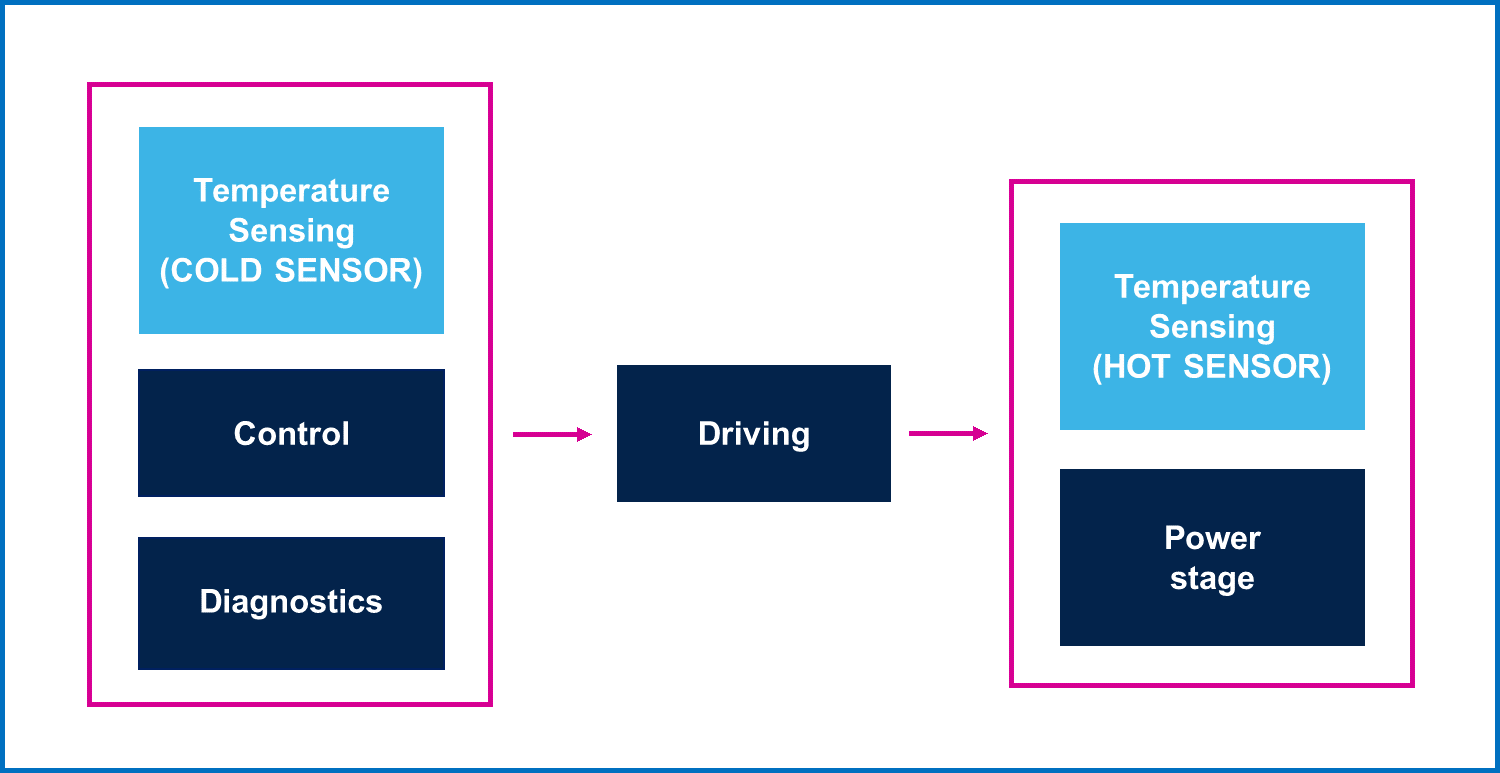 Fig. 1 Simplified block diagram of a smart switch with different temperature sensors.
The temperature sensors are implemented using polysilicon diodes thanks to their linear temperature coefficient across operating temperatures. The cold sensor is positioned in the cold zone of the driver near the controller, while the hot sensor is placed in the power stage area, which is the hottest zone in the driver.
Using this double-sensor technique enables the driver’s temperature increase to be limited since the thermal protection is triggered when the lowest temperature value between the over-temperature threshold and a dynamic temperature level between the sensors is reached. Once removed the overtemperature fault, the smart switch can be reactivated when the temperature decreases to a fixed value.
This significantly helps to reduce thermal fatigue in terms of thermo-mechanical stress on the switch, which can accumulate over time and lead to degradation and reduced reliability.
Thermal Mapping
Along with simulation and prevention procedures, infrared (IR) thermography is a valuable technique to obtain detailed thermal maps of the driver, which provide a comprehensive understanding of the heat distribution within the integrated circuit, highlighting any potential hazard.
To assess the effectiveness of intelligent protections in harsh automotive applications, the heat distribution within the driver has to be analyzed under challenging short-circuit conditions with two different scenarios:
- Terminal Short-Circuit (TSC);
- Load Short-Circuit (LSC).
The terminal short-circuit condition occurs when a low resistance connection between the terminals of a component or device is present, as shown in Fig. 2.
 Fig. 2 Testing circuit for temperature measurement under TSC.
On the other hand, a load short-circuit condition arises when there is an inductive path between the load and the power source, leading to a sudden surge in current flow (Fig. 3).
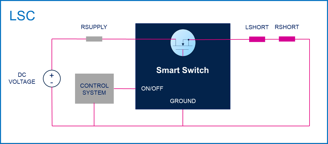 Fig. 3 Testing circuit for temperature measurement under LSC.
The following test conditions are considered:
- Tamb = 25 °C
- Vbat = 14 V
- Ton = 1 ms for mapping
- Ton = 300 ms for temperature acquisition of thermal sensors and hot spots
- TSC condition: RSUPPLY = 10 mΩ, RSHORT = 10 mΩ
- LSC condition: RSUPPLY = 10 mΩ, LSHORT = 5 µH, RSHORT = 100 mΩ
where Tamb is the ambient temperature
Vbat the DC battery voltage
Ton the time duration of the short-circuit event
RSUPPLY the resistance of the battery
RSHORT the short-circuit resistance
LSHORT the short-circuit inductance.
In order to generate a temperature map, the IR camera sensor is utilized to capture the infrared emissions at each location, which are then converted into temperature values. To ensure the conversion accuracy from specific colors to defined temperature values, a calibration process is essential. This process involves comparing the different colors obtained from the sensor with known temperature values, which can be obtained through specific thermal sensitive parameters and their trend versus temperature increase. By analyzing these parameters, the calibration process can ensure that the temperature map accurately reflects the temperature distribution in the area being scanned.
To calibrate the IR camera sensor, the forward voltage (VF) of the MOSFET’s body drain diode is chosen due to its linear dependence on temperature. However, a pre-calibration of the diode is necessary to accurately determine its temperature coefficient. This is achieved by measuring the VF voltage at a constant forward current (IF) while varying the temperature from 25°C to 100°C. To prevent any temperature rise caused by the current and its associated power dissipation, the IF value is selected within the range of 10mA to 20mA.
The VF values collected at different temperatures can be used to perform a linear interpolation and mathematical fitting to obtain the temperature coefficient of the diode, as shown in Fig. 4.
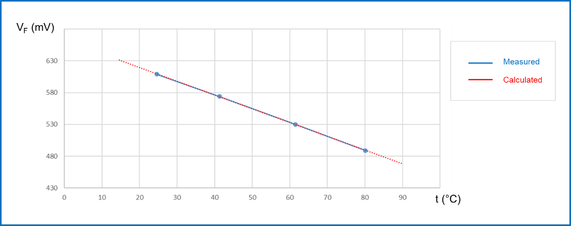 Fig. 4 Pre-calibration of MOSFET’s body drain diode.
Calculations are made through the following equation (1):
Dt = DVF /K (1)
where:
Dt is the temperature variation;
DVF the forward voltage variation;
K is the temperature coefficient of the diode.
The temperature map is created by acquiring each temperature point through an IR camera sensor at 1ms intervals. Once all the die points are acquired (which takes around 3000 seconds), a specialized software generates the map, which depicts the temperature of each point based on the minimum spatial resolution of the IR sensor. By overlaying the thermal map onto the row silicon die picture, it is possible to identify the hottest points in the active area and determine their coordinates while the current flows through the device.
As an example, the thermal maps for the dual-channel VND9012AJ smart switch are depicted in Fig. 5 under TSC conditions.
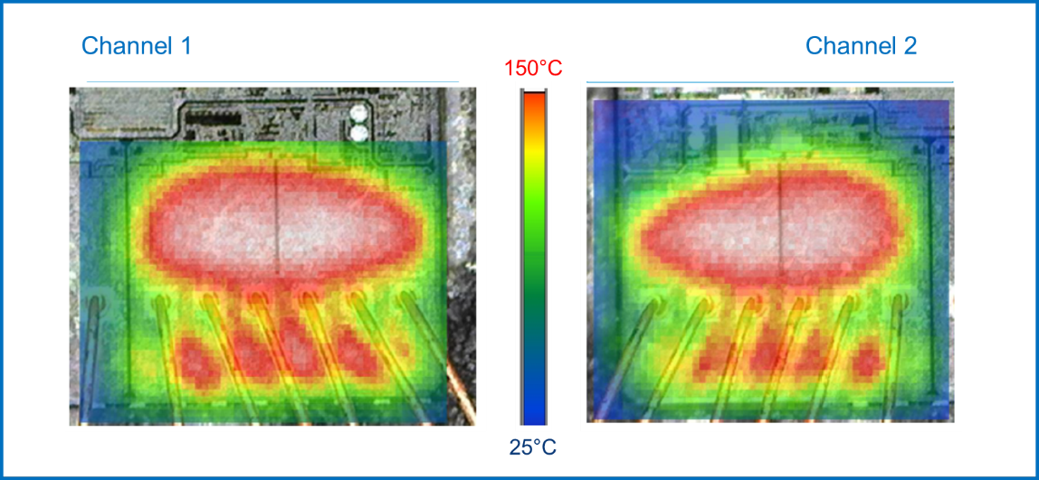 Fig. 5- Thermal maps for VND9012AJ channels under TSC condition.
The graphical representation of temperature distribution across the driver’s channels, depicted through varying colors within the temperature range of 25°C to 150°C, serves as a crucial aid in detecting any regions experiencing excessive heat and ensuring the driver’s safe temperature operation. The provision of thermal maps for each channel under diverse operating conditions enables the tests to authenticate the driver’s reliable functioning without surpassing its maximum temperature threshold.
In order to locate the hot spots and monitor the temperature evolution for both hot and cold sensors, and subsequently validate the efficacy of the thermal shutdown mechanism, a longer short-circuit duration of 300ms is taken into account.
The temperature variations observed in VND9012AJ while undergoing TSC are displayed in Fig. 6.
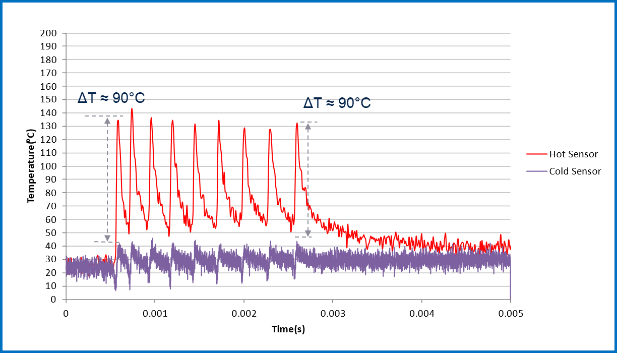 Fig. 6- Temperature variations for both sensors under TSC condition.
The graph indicates the presence of hot spots in both channels of VND9012AJ as detected by the hot sensors, and the maximum temperature of these hot spots is in the range of 150 °C.
The thermal maps for VND9012AJ under LSC conditions are presented in Fig. 7.
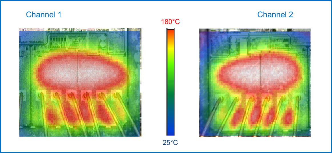 Fig. 7- Thermal maps for VND9012AJ channels under LSC condition.
The temperature variations observed in VND9012AJ while undergoing LSC are displayed in Fig. 8.
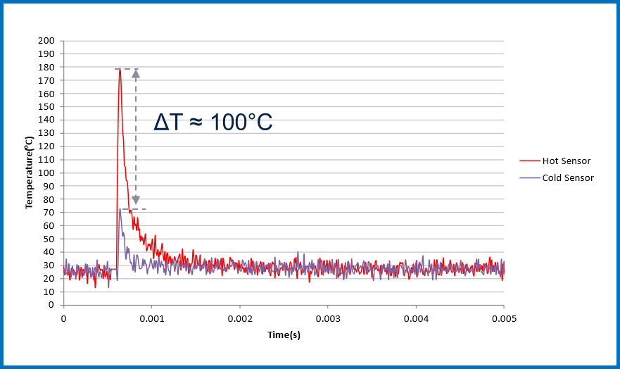 Fig. 8 Temperature variations for both sensors under LSC condition.
Both conditions trigger the thermal protection mechanism, causing the current to be limited to a safe level.
Conclusions
Valuable insights into the design and operation of the smart switch have been obtained through experimental results, particularly regarding current distribution and thermal protection mechanisms. It is essential to maintain a well-balanced behaviour of all channels to create an intelligent driver that improves safety and reliability in automotive systems. The use of IR thermography enables a precise and comprehensive analysis of temperature distribution, which enhances the smart switch’s thermal sensing and protection system. In demanding automotive environments, swift activation of these protections is crucial to detect overheating and prevent any potential harm to the device or system.
References
[1] P. Meckler and F. Gerdinand, “High-speed thermography of fast dynamic processes on electronic switching devices”, 26th International Conference on Electrical Contacts (ICEC 2012), 2012.
[2] X. Zhou and T. Schoepf, “Detection and formation process of overheated electrical joints due to faulty connections”, 26th International Conference on Electrical Contacts (ICEC 2012), 2012.
[3] T. Israel, M. Gatzsche, S. Schlegel, S. Großmann, T. Kufner, G. Freudiger, “The impact of short circuits on contact elements in high power applications”, IEEE Holm Conference on Electrical Contacts, 2017.
[4] Y. Lozanov, “Assessment of the technical condition of electric contact joints using thermography”, 17th Conference on Electrical Machines, Drives and Power Systems (ELMA), 2021.
[5] M. Bonarrigo, G. Gambino, F. Scrimizzi, “Intelligent power switches augment vehicle performance and comfort”, Power Electronics News, Oct. 10, 2023.
The post Balancing Currents for Optimal Performance in Automotive Smart Drivers appeared first on ELE Times.
Pages

