
ELE Times

TATA in Partnership with Satellogic Launches First Made in India Military Satellite
Tata Advanced Systems Ltd, a subsidiary of TATA Sons, in collaboration with Satellogic has successfully launched India’s first private sector-built sub-metre resolution earth observation satellite, TSAT-1A from the Kennedy Space Centre, Florida through SpaceX’s Falcon 9 rocket on April 7.
The TSAT-1A satellite assembled at TASL’s Karnataka facility represents a significant milestone in space technology. Its deployment as part of SpaceX’s inaugural Bandwagon flight, which also deployed a total of 11 satellites, underscores its importance in the realm of space exploration and satellite deployment.
The satellite is anticipated to bring about a paradigm shift in satellite imaging due to its high-resolution capabilities and rapid data delivery. Its configuration in low-earth orbit, coupled with its lightweight design of less than 50 kg, positions it as a versatile asset capable of serving a wide range of applications. Its potential impact on various sectors including defense and communication, makes it a pivotal development in the field of space technology.
The post TATA in Partnership with Satellogic Launches First Made in India Military Satellite appeared first on ELE Times.
Semiconductors beyond nanometers
SCHUMACHER | Infineon Technologies AG
In today’s world, semiconductors are essential components of our everyday lives and the backbone of our economies. From the devices we use to communicate to the machines that power our factories, semiconductors are the building blocks that enable digitalization and decarbonization. However, public and policy debates about semiconductors often focus solely on their smallest feature size, measured in nanometers, which fails to capture the full complexity and importance of these high-tech goods.
At Infineon, we have developed a simple yet powerful way to understand semiconductors – our “Semiconductor Tree.” This intuitive structure provides a framework for discussing the different branches of the semiconductor industry, from power semiconductors to memory chips and microcontrollers. By exploring each branch of the tree, we can gain a better understanding of the unique properties and specialized industries that each one represents.
First transistor (1947)At the core of the semiconductor industry is the transistor switch, which was first demonstrated in 1947 by a team of researchers at AT&T Bell Labs. Since then, we have seen an exponential miniaturization roadmap, which has led to microprocessors that contain billions of transistors. However, this race to shrink transistors and integrate them as densely as possible into an Integrated Circuit (IC) requires extreme ultraviolet light and the most complex machines ever manufactured by mankind.
Power semiconductors
Notably, one branch of the semiconductor industry has focused on optimizing the individual transistor for faster switching and/or switching of ever-higher electrical power. These are known as power semiconductors and are becoming increasingly important as societies and economies move towards electrification as a means to decarbonize. Power semiconductors require sophisticated control of the underlying technologies and processes, and leading companies often control much of the value chain in-house.
Infineon’s power semiconductor business is an example of an Integrated Device Manufacturer (IDM), with major manufacturing sites in Germany, Austria, and Malaysia.
Memory, microcontrollers/microprocessors, and analog/mixed-signalAnother path to optimizing the transistor was to standardize it as much as possible, shrink it, and pack it as densely as possible. This gave rise to other branches in the semiconductor tree, including memory, microcontrollers, and microprocessors. Each of these branches has its unique properties, requirements, and industries. For instance, memory semiconductors allow storage and read-out of information in the form of electrical signals.
Microcontrollers, on the other hand, control everyday devices like washing machines, cars, airplanes, and industrial control systems. Analog/mixed-signal semiconductors act as the interface between our real world and the digital world, processing analog electrical signals like WiFi, Bluetooth, or radar chips for autonomously driving cars. Since analog signal processing doesn’t follow the same shrink path as analog, manufacturing analog/mixed signal today is often done at a sweet spot of 130-90nm.
Final ThoughtsThe world of semiconductors is vast and diversified, and it is crucial to have a more nuanced understanding of the importance and development of the respective industries. Semiconductors are essential building blocks for our personal lives, modern societies, and economies, and their importance will only grow as we continue to digitize and decarbonize.
As such, it is no surprise that semiconductors are at the center of global politics. By understanding the complexity and importance of semiconductors, we can have more precise discussions about their role in shaping our world.
The post Semiconductors beyond nanometers appeared first on ELE Times.
Examining an Air Filter with a RANS Turbulence Model
Joseph Carew | Comsol
HVAC systems do more than provide the smooth, chilled air that flows when the temperature outside rises. Within these systems, air moves through filters to ensure high air quality. With clean air at stake, modeling and simulation can be used to gain an in-depth understanding of the physics behind the behavior of air as it moves through a filter…
Modeling an Air FilterThe filters within HVAC systems rely on a material (often fiberglass or cotton folds) capable of straining the air and catching particulates like dust, pollen, and bacteria. These materials impact the flow of the air, catching the unwanted particulates while simultaneously allowing the filtered air to flow through. Modeling these devices and the turbulent flow they induce allows for determining the effectiveness of different materials when they are used for filters, helping designers to narrow down the material options before investing in real-life, experimental versions.
In this blog post, we will look at a common air filter geometry (shown below) as our example.
Modeling this air filter begins with the CFD Module, an add-on product to the COMSOL Multiphysics® software, which enables users to create Reynolds-averaged Navier–Stokes (RANS) turbulence models in open and porous domains. In this example, the air filter is modeled as a highly porous domain with 90% of the material occupied by cylindrical pores with a diameter of .1 mm. The support of the air filter is represented by a frame with no-slip walls. For this example, we employed the Turbulent Flow, k-ω interface because of its accuracy for models with many walls, including no-slip walls. (An in-depth look at the model setup can be found in the model documentation, which can be accessed via the button at the end of this blog post.)
Evaluating the ResultsSolving the model allows for visualizing the change in turbulence, velocity, and pressure as air moves toward, through, and past the filter. The computation begins with the air moving toward the filter (purple in the image below). When the air passes through the filter, the interstitial velocity increases (although the porous-averaged velocity remains constant), resulting in an increase in turbulence kinetic energy. Additionally, there is an abrupt pressure drop due to the increase in velocity and the increased friction and pressure losses, which stem from the high number of wall surfaces. As for the behavior of the air as it moves away from the filter, the frame of the filter prevents the air from moving freely, instead causing downstream wakes of air.
The visualization of the air moving through the filter can be used to conclude whether or not the filter will remove contaminants from the air. To confirm this conclusion, the solution can be evaluated with different slice plots. One of the slice plots for this example indicates that the velocity of the air is most impacted by the porous air filter and the frame and that it homogenizes through the wake region. A slice plot measuring the turbulence kinetic energy shows that the turbulence kinetic energy peaks noticeably within the filter and attains typical values on the no-slip walls.
In general, the model points to a pressure drop and a dramatic increase in turbulence within the filter, creating perturbations in velocity perpendicular to the main direction of the flow thus also increasing the probability of the particles to collide with the pore walls and stay there. In other words, the increase in turbulence provides the mixing required for filtering out the unwanted particulates, which otherwise would flow through the pores undisturbed.
The post Examining an Air Filter with a RANS Turbulence Model appeared first on ELE Times.
Broadcom brings together two proven portfolios to deliver complete hybrid cloud cybersecurity
Rob Greer, Vice President and General Manager, Enterprise Security Group, Broadcom
Merging Carbon Black with Symantec forms the new Enterprise Security Group at BroadcomIt is clear, there is no let-up in cyberattacks, so the timing could not be better for Broadcom to bring Carbon Black and Symantec together. These engineering-first, innovation-centric brands are both committed to delivering proven cybersecurity solutions and support built to meet the unique and highly complex challenges of the largest and most heavily regulated enterprise customers and partners. Broadcom will make significant investments in both brands, and continue to offer both portfolios under the Enterprise Security Group business unit. Our joint mission is to help secure the world’s largest and most advanced enterprises.
Symantec’s portfolio, with some of the best security technology and research in the world, concentrates on data and network protection, while Carbon Black’s complimentary portfolio specializes in both endpoint detection and response (EDR) and application control. Bringing both network and data telemetry to Carbon Black will enable greater visibility and control for our joint customers. Under the new Enterprise Security Group, customers will continue to receive the best service with more dedicated resources and focused support than ever before. What can you expect in the near-term? Let’s take a closer look at innovation, customers, and partners.
InnovationBroadcom’s financial stability empowers Symantec and Carbon Black product portfolios to innovate at a massive scale. Our customers will benefit from access to an enhanced enterprise-grade portfolio and leading technological advancements, with unparalleled service and support.
Initially, we will invest in R&D to improve – and extend the life — of the products our customers are using both on-prem and across hybrid clouds. We also are excited about the complementary nature of both sets of technologies and the combined value they will provide our customers, opening up more choices. For example, Symantec has a data center security product to protect traditional workloads in the data center. Carbon Black has a complementary solution. With access to these two technology sets, defenders will be even better equipped to protect their infrastructures.
On the talent side, we will be making significant investments in engineering. Carbon Black is known for its outstanding, customer-centric engineering capabilities, and we are committed to investing in Carbon Black’s incredible franchise and putting the best talent in the best roles. For example, both Carbon Black and Symantec have existing engineering sites in India. While we see the opportunity to converge them, we do not expect to make headcount reductions in those sites. In fact, we plan to make more investments in India. In addition, we will continue to invest in support and R&D for both brands, retaining key technical and product leaders to ensure continued success today and in the future.
CustomersSymantec and Carbon Black product portfolios will continue to operate in their current states for the immediate future. Our customers can expect to gain access to an extensive and robust enterprise-class portfolio supported by top-tier security experts, intelligence, and continued innovation, all backed by the financial stability of Broadcom.
Looking ahead, we will explore innovative new ways to deliver solutions to our customers. This will involve intensely focusing on the technologies that provide the most value to our customers and partners and invest more resources in those areas so our customers realize even greater value and ROI.
PartnersAt Broadcom, we take a very focused go-to-market approach. As Hock Tan, our CEO, says, “We do what we do best.” By focusing on our core strengths and not trying to be all things to everyone, we open big opportunities for our partners to step in, fill gaps, and profit from them. The addition of the Carbon Black portfolio provides a great opportunity for our partners to drive more revenue, win more customers, and grow. Broadcom will provide the necessary training, support and other resources to ensure our partners’ success with Carbon Black solutions. For examples of our breakthrough approach to building a highly scalable, close-to-the-customer partner ecosystem, look no further than our Global Cybersecurity Aggregator Program (GSAP) and the Expert Advantage Partner Program. Partners in these programs deliver high-value services to customers of all sizes – including our largest enterprise accounts.
Building a strong security futureOver the next few weeks, we will be sharing more details about how today’s announcement will further benefit our customers and partners. In the meantime, we encourage you to visit our online resources to access additional information. As ransomware attacks and other cybersecurity threats continue to rise, you can be rest assured that Carbon Black and Symantec together will provide the mission-critical technologies to defend the most complex, highly regulated organizations.
The post Broadcom brings together two proven portfolios to deliver complete hybrid cloud cybersecurity appeared first on ELE Times.
element14 brings latest Silex Wi-Fi 6 Radio Development Kit from Gateworks to Industrial Developers Worldwide
element14 will be the only distributor to offer this kit for sale at Embedded World 2024.
element14 has announced the availability of Gateworks’ latest Wi-Fi 6 Development Kit – GW11048-5-A.
Gateworks will showcase its cutting-edge technology kit during the Embedded World 2024 exhibition in Nuremberg, Germany, from the 9th to 11th April. element14 has been chosen as the exclusive distributor of the kit, making it the only place where customers can purchase it during the event.
The Wi-Fi 6 Development Kit is designed to facilitate the validation of the Silex SX-SDMAX and SX-PCEAX Wi-Fi 6 radios, providing developers with a seamless out-of-the-box evaluation experience. It delivers ruggedized wireless connectivity for a diverse range of industrial applications, from remote real-time monitoring to predictive maintenance and enhanced logistics.
This latest innovation comes with a pre-loaded Linux system and all the necessary accessories to get started quickly.
Key features include:
- Supports Silex SX-SDMAX and SX-PCEAX Wi-Fi 6 radios (radios not included)
- Includes Venice GW7200 Single Board Computer (SBC) with pre-loaded Linux drivers
- Onboard NXP i.MX8M Mini processor (1.6 GHz quad-core)
- 8GB eMMC flash storage and 1GB LPDDR4 DRAM
- Two Gigabit Ethernet ports and two Mini-PCIe expansion slots
- Multiple connectivity options including MicroSD, Nano SIM, I2C, SPI, and serial ports
- Real-time clock, voltage and temperature monitoring
- Wide input voltage range (8 to 60VDC) with PoE support
- Operates in temperatures ranging from -40°C to +85°C
“We are thrilled to provide Gateworks’ WI-FI 6 development kit to our customers. This cutting-edge technology is a game-changer for those seeking to develop and deploy IoT applications and systems. We look forward to seeing its capabilities showcased at the exhibition and support our customers with all their development needs”, said Romain Soreau, Head of Single Board Computing at element14.
In addition to the Wi-Fi 6 Development Kit, element14 also offers Gateworks Corporation’s complete line of products for industrial applications.
Gateworks will be highlighting their line of railway solutions at Embedded World, aimed at enhancing the efficiency and safety of rail yards, such as rugged Gateworks Single Board Computers (SBCs) combined with a variety of wireless options such as high-precision GNSS Mini-PCIe cards. These solutions enable capabilities such as centimetre-level accuracy in tracking and monitoring critical data, streamlined yard operations and enhanced customer service for rail operators.
The post element14 brings latest Silex Wi-Fi 6 Radio Development Kit from Gateworks to Industrial Developers Worldwide appeared first on ELE Times.
Designers lead advances in CT scanning field
Courtesy: Avnet
When a doctor tells you to get a CT scan, they’re calling on a powerful medical imaging technology for insights only otherwise possible through invasive procedures.
Computed tomography (CT) exploits the penetrating nature of X-rays. A standard X-ray shines a 2D beam of high-energy photons through the subject. How these photons are detected has changed over the years. It was once just photographic film, but today it is more likely to be a digital detector.
Since bone, muscle and fat each absorb X-rays differently, the image captured is effectively the shadow cast by the mix of tissues in the body. Rather than create an image directly from the photons detected, computed tomography processes that captured data to synthesize an image.
In CT scanning, a source illuminates the subject using a fan-shaped beam of X-rays that are picked up by an arc-shaped array of digital detectors. The source and the detector are mounted on a circular gantry, which rotates around the patient, taking scans from multiple angles.
The resulting scans are not directly interpretable as an image. The scans are combined in a computer, creating a more detailed 2D “slice” through the body. Many CT scanners also coordinate the movement of the patient with the gantry’s rotation, creating a sequence of slices through the body that can be processed into a 3D image.
Seeing the advantages of CT in medical imaging Figure 1: Computed tomography is an advanced medical imaging technology. New developments are making it even more useful for healthcare professionals and safer for
patients.
CT scans can render more detail about internal structures than ordinary X-rays and can present that data in augmented 2D or 3D, making it easier to interpret. They are also relatively fast, which makes them useful for providing insights about injuries to the head, spine, chest, abdomen and pelvis.
The ability to post-process CT images means that they can provide a useful basis for detecting tumors and cancers, their size, location, and how they have spread. They can also reveal internal bleeding and the spread of infection as well as enable doctors to visualize blood vessels, aneurysms and blockages throughout the body.
CT imaging can be used to reduce the invasiveness of some procedures. The ability to differentiate diseased tissue helps surgeons avoid removing healthy tissue unnecessarily. Similarly, the 3D detail possible with CT imaging can provide a useful basis for planning procedures such as biopsies, surgery, implants, and radiation treatment.
The technique can reveal the detailed health of bones and joints, making it easier to understand wear or disease and to diagnose fractures. CT scans can also help track the progress of disease and reveal the effectiveness of treatments such as chemotherapy.
There are challenges associated with CT scanning. They usually involve greater exposure to ionizing radiation than is common with standard X-rays. Patients may also react badly to the contrast agents used to improve the CT scan’s effectiveness.
Navigating the key trade-offs in CT scanner design Figure 2: CT scanning is a non-invasive solution to seeing inside the body. It can reveal vital details for healthcare professionals but there are still areas for improvement.
Developers of CT scanners work with two forms of constraints. The first is the paramount nature of combining innovation with patient safety when using ionizing radiation. The second is the tension that can bring for patients and care providers. The availability of new technologies and capabilities must always be met with the best judgment and a conservative attitude.
There are technical trade-offs in CT design too. Perhaps the most important of these is between image quality and radiation dose levels. Higher doses may improve image clarity at the cost of greater exposure. Technologies such as iterative image reconstruction and denoising algorithms based on machine-learning techniques can now replicate some of the image-quality gains of high-dose scans at lower doses.
Trade-offs also exist between the speed of scanning and image resolution. Faster scanning reduces artifacts introduced by patient movements but can result in lower spatial resolutions. Scanning more slowly can deliver higher resolution if the patient is still for long enough.
Designers also need to decide which market niche they want to address. For example, designing a scanner with a large field of view makes it easier to scan large body parts, but requires larger, more expensive detector arrays. Other trade-offs may have to be made between scanner flexibility and specialization, hardware quality and maintenance costs, and software capabilities and reliability.
There are also financial considerations over initial cost and long-term upgradability. Buying a CT scanner means a large upfront outlay and substantial operating costs. Buyers may be prepared to choose a scanner engineered to evolve, rather than a lower-cost machine with a more limited useful lifetime.
 Figure 3: CT scanner represent a significant capital outlay. New technologies are tackling the ROI on machines, with capability and longevity in mind.
Making innovations in CT design
Figure 3: CT scanner represent a significant capital outlay. New technologies are tackling the ROI on machines, with capability and longevity in mind.
Making innovations in CT design
Despite the constraints and trade-offs outlined above, there are many avenues for innovation in CT design. Each detector usually has a scintillator, which emits visible light when it is hit with X-rays, mounted over a digitizing photodetector circuit. A basic CT scanner will have one arc of these detectors, but more sophisticated variants will have multiple arcs so that they can sample multiple “slices” simultaneously. There may be as many as 256 arcs.
To support the high number of detectors, semiconductor companies are engineering 128-channel analog-to-digital converters (ADCs). These ADCs can be mounted in modules to produce 256-channel capabilities. The chips have low-power, low-noise, low-input-current integrators. Simultaneous sample-and-hold circuits ensure that all samples are taken at once. Some ADCs targeting medical applications offer resolutions of up to 24 bits.
Achieving low-dose CT imagingDifferent beam energies can reveal different things about the subject they are illuminating. Radiologists can adjust the beam strength used in the scan to pick out specific details. This is called the spectral CT technique.
Another approach is to use a dual-layer detector, with the top layer absorbing the lower-energy X-ray photons and a lower layer absorbing the higher-energy photons. This technique can reveal more about how the X-rays have been affected by their passage through the subject material.
A further innovation involves single-photon capture detection, in which a semiconductor device is used to directly count each X-ray photon. This gives scope for lower-dose CT imaging, since it does away with potential photon losses in the scintillation process of conventional detectors. It also makes it possible to measure the arrival energy of every photon, again giving greater insights into how it has been affected by passing through the patient.
In dual-source CTs, two source/detector array pairs are mounted on the rotating gantry ring at 90 degrees to each other. This arrangement gives good coverage of the patient while minimizing interference between the sources.
The two sources can run at different energies, which brings the advantages of spectral CT discussed above. They can also acquire a whole slice image more quickly than a single-source scanner, which gives them greater temporal resolution for imaging moving features such as a beating heart. This in turn reduces motion artefacts in the final scan. Faster scans may also be more acceptable to some patients.
Developing high-resolution CT scannersHigh-resolution CT scanners produce very thin slices of less than 1 mm. They use more, smaller detectors, to achieve higher spatial resolutions than standard scanners. The extra resolution makes it easier to detect and characterize small features accurately.
Such scanners usually have sophisticated image-reconstruction algorithms to enhance image quality and detail, which is particularly important for visualizing fine structures and edges. They can also have features such as enhanced X-ray beam management. These techniques give higher contrast images than standard scanners.
CT scanners are enormously valuable for producing insights into patient health without the need for invasive procedures. Their developers can call on rapidly evolving technologies, such as detector electronics and machine-learning techniques, to provide enormous scope for innovation. Responsibility for patient safety means the adoption of new technologies can feel slow.
Fortunately, designers can make a real difference here by exploring the systemic trade-offs involved in the development of novel CT scanners to produce capabilities that are engineered to encourage rapid uptake. For example, designing a detector sampling and digitization circuit with a lower noise floor will enable higher-resolution scans at the same beam energy, or similar resolutions at lower doses.
An FPGA accelerator board may be used to speed up image-processing algorithms, increasing the scanner’s throughput and so cutting the cost of individual scans. Or perhaps there’s a better way to manage power use in the scanner, extending its reliability and so cutting its operating costs.
Avnet recognizes the holistic challenge of developing medical imaging products and has the resources to help OEMs address them.
The post Designers lead advances in CT scanning field appeared first on ELE Times.
Infineon PSOC Edge E8x microcontrollers are the first devices designed to meet the new PSA Level 4 certification requirements
With embedded security considered to be a vital aspect in the deployment of Internet of Things (IoT) applications, Infineon Technologies AG has announced that its new PSOC Edge E8x MCU product family has been designed to meet the highest certification level provided by the Platform Security Architecture (PSA) Certified program, a framework for embedded security. The PSA Certified Level 4 device certification is targeted by implementing an on-chip, hardware-isolated enclave that provides secured boot, key storage and crypto operations in all PSOC Edge E8x devices.
“By aspiring to achieve this robust embedded security certification, IoT designers for edge applications such as wearables and smart home applications can be confident their products can achieve highest levels of security,” said Erik Wood, Senior Director Product Security for IoT, Computer and Wireless business, Infineon Technologies. “Integrating hardware security on the MCU also unlocks new edge computing markets such as printers and payment terminals that previously required discrete security chips. As a security leader, we are committed to enabling designers to reach the highest level of security for all applications.”
PSA Certified is a security framework established by Arm and industry partners in 2019. It provides both design guidelines and independent security evaluations through third-party labs intended to assure that all connected devices are built upon a Root of Trust. PSA Certified certifications achieved by an MCU extend through the value chain, allowing device builders and application providers to reuse that certification as they deploy products in the field.
“Connected device security is critical to scaling IoT deployments, and something that Arm and its ecosystem is committed to continuing to drive through initiatives like PSA Certified,” said David Maidment, Senior Director, Secure Devices Ecosystem at Arm. “We applaud Infineon’s ongoing commitment to robust device security by striving to achieve PSA Certified Level 4 iSE/SE for its new family of MCUs.”
The post Infineon PSOC Edge E8x microcontrollers are the first devices designed to meet the new PSA Level 4 certification requirements appeared first on ELE Times.
Transforming Manufacturing with Digital Twins
Sometimes, the tech buzzwords of the moment are used so freely when speaking to colleagues and customers and read daily in articles, on social media, and even in the mainstream news. Although terms such as AI, gen AI, edge computing, digital twins, IoT, and sustainability are familiar, their practical implementation is challenging. The challenges and obstacles are numerous and, at times, unique to specific use cases or organizations and depend on the maturity of the emerging technology.
Consider digital twins as an example; what are they, and what is all the hype surrounding them? The definition used by the Digital Twin Consortium describes a virtual representation of real-world entities and processes synchronized at a specified frequency and fidelity with the capability of transforming business by accelerating holistic understanding, optimal decision-making, and effective action. Digital twins use real-time and historical data to represent the past and present and simulate predicted futures. Furthermore, digital twins are motivated by outcomes, tailored use cases, powered by integration, built on data, guided by domain knowledge, and implemented in IT/OT systems.
Suppose we take a manufacturing plant as an example. Whether the equipment used is of new generation or legacy and has fixed function, general-purpose devices, or a combination, one thing is for sure: an overwhelming amount of data is produced. The data is a modern-day goldmine if extracted, processed, aggregated, and verified. Data allows digital twins to thrive, and its integrity is one of the most critical aspects of the technology. It is what helps ensure consistent, accurate, reliable results. In the future, IT and OT resources and infrastructure will need to converge further to standardize, transform, and apply data insights in manufacturing settings.
The accuracy of the data allows us to rapidly create physically precise, virtual 3D models and replicate real-world environments, from the factory floor to stores and cities.
Digital twins can be used to recreate the factory itself, allowing organizations to monitor and make changes in the digital environment to verify the impact of results before making changes on the factory floor. Manufacturers can also create an exact digital replica of their product and carry out true-to-world testing, allowing them to find and correct issues or errors and make optimizations before moving into production. Furthermore, digital twins create predictive models based on data points and their historical changes. They are measuring conditions against historical patterns and trends to identify anomalous behaviour, such as production line bottlenecks or potential safety and security breaches, right down to granular details, such as the temperature and vibration of a single appliance.
Considering today’s level of technological maturity, digital twins provide a range of benefits, including:
- Heightened visibility and transparency into assets and environments
- Reducing costs, time, and effort in changing production workflows
- Reducing material waste and delivering energy and other utility savings
- Sustainability
- Efficient acceleration of production times
- Reduced errors and issue resolution in pre-production phase
- Employing machine learning models that can understand and act in real-world situations.
Digital twins generally require purpose-built software on IoT edge servers that draw real-time data from sensors, appliances, and cameras. However, in most cases, organizations can start with their existing infrastructure and layer analytic tools to leverage the data already generated by installed equipment. Incrementally adding compute resources will help improve the accuracy of the digital twin over time. These considerations depend on what the organization is trying to achieve and its long-term goals. Technology is a strategic investment, so organizations should work with a reliable collaborator to plan for new use cases from infrastructure, resource, and security aspects.
The skill sets needed to leverage modern technology have evolved, and the workforce needs to evolve with that to obtain optimal results.
 ROLAND DUCOTE
Director, Sales Intelligent Solutions,
OT + Emerging Accounts,
Arrow Electronics, Inc.
The post Transforming Manufacturing with Digital Twins appeared first on ELE Times.
AURIX TC4x microcontrollers for embedded AI application development receive safety assessment from Fraunhofer IKS
In the automotive industry, embedded AI is becoming increasingly important for safety-critical real-time applications. However, this also creates new requirements and standards that must be considered during the complete product lifecycle. Infineon Technologies addresses these new requirements with the AURIX TC4x microcontroller (MCU) family, which meets the AI-specific safety requirements to achieve SAFE AI compliance, as proposed by the Fraunhofer Institute for Cognitive Systems IKS. The MCUs, with their ASIL-D compliant AI accelerator (PPU), provide an innovative platform for developing embedded AI-based use cases and automotive applications such as motor control, battery management systems, vehicle motion control and siren detection.
The SAFE AI framework based on ISO PAS 8800 and current state-of-the-art AI regulations is an evaluation methodology developed by Fraunhofer IKS that assesses the trustworthiness of AI in terms of robustness, data utility, operational design domain (ODD) and environmental conditions. The functional safety measures of the AURIX TC4x family thus provide mechanisms for compliance with AI regulations and standards at the application level. By using the AURIX TC4x family, car manufacturers can assess the safety and reliability of AI solutions and identify potential vulnerabilities during system development and operation. For safety-critical real-time applications, the use of AI models like neural networks increases accuracy and provides additional safety in conjunction with the existing physical sensor.
“The integration of safe and reliable AI functionality into automotive microcontroller families is essential to further improve vehicle performance, safety, and comfort,” said Thomas Boehm, Senior Vice President Microcontroller at Infineon. “We are therefore very proud that our AURIX TC4x microcontroller has successfully passed the SAFE AI assessment by the Fraunhofer Institute for Cognitive Intelligence. This underlines our position as one of the leading innovation drivers in the industry.”
The post AURIX TC4x microcontrollers for embedded AI application development receive safety assessment from Fraunhofer IKS appeared first on ELE Times.
Renesas Introduces New Entry-Level RA0 MCU Series with Best-in-Class Power Consumption
Low-Cost Devices Target Consumer Electronics, Small Appliances, Industrial System Control and Building Automation
- Core: 32MHz Arm Cortex-M23
- Memory: Up to 64KB integrated Code Flash memory and 12KB SRAM
- Analog Peripherals: 12-bit ADC, temperature sensor, internal reference voltage
- Communications Peripherals: 3 UARTs, 1 Async UART, 3 Simplified SPIs, 1 IIC, 3 Simplified IICs
- Safety: SRAM parity check, invalid memory access detection, frequency detection, A/D test, immutable storage, CRC calculator, register write protection
- Security: Unique ID, TRNG, Flash read protection
- Packages: 16-, 24- and 32-lead QFNs, 20-pin LSSOP, 32-pin LQFP
The post Renesas Introduces New Entry-Level RA0 MCU Series with Best-in-Class Power Consumption appeared first on ELE Times.
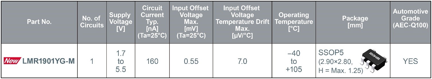
ROHM Develops a New Op Amp that Minimizes Current Consumption
Industry-low 160nA current consumption improves power savings in consumer and industrial equipment
ROHM has developed a linear operational amplifier (op amp) – LMR1901YG-M – featuring the lowest* current consumption in the industry. This makes it ideal for amplifying sensor signals used to detect and measure temperature, flow rate, gas concentration, and other parameters in applications powered by internal sources (i.e. batteries).
In recent years, advanced control has been in increasing demand for various applications in consumer and industrial electronics. Therefore, there is an increasing need for accurate sensing of parameters relevant to the application – such as temperature, humidity, vibration, pressure, and flow rate. Op amps whose main function is to amplify sensor signals for subsequent detection and/or analog-to-digital conversion, is a crucial component in the signal chain – greatly affecting both accuracy and power consumption. ROHM is developing op amps that satisfy the dual need for high accuracy and low current consumption. By further refining the circuit design based on original Nano Energy technology, ROHM is now able to offer an op amp that delivers the lowest current consumption on the market.
The LMR1901YG-M leverages original ultra-low power technology that thoroughly suppresses current increase caused by temperature and voltage changes to reduce current consumption to just 160nA (Typ.) – approximately 38% lower than that of general low power op amps. This not only extends the life of applications powered by internal batteries like electronic shelf labels, but also contributes to longer operating times for smartphones and other devices equipped with rechargeable batteries. At the same time, this low current consumption does not change over the temperature range of -40°C to +105°C – allowing stable low-power operation, even in environments where external temperatures fluctuate, including fire alarms and environmental sensors.
Other performance enhancements include 45% reduction of input offset voltage to just 0.55mV (Max. Ta=25°C) over general low-current op amps while a maximum input offset voltage temperature drift of 7V/°C is guaranteed. This enables high-accuracy amplification of sensor signals. Capable of operating from 1.7V to 5.5V supply voltage and offering rail-to-rail input/output, LMR1901YG-M is suitable for a wide variety of applications in the industrial equipment and consumer markets. ROHM’s new op-amp also complies with the automotive reliability standard AEC-Q100 – ensuring stable operation even under harsh conditions such as vehicle cabins without compromising functionality.
In addition to various technical documents necessary for circuit design and SPICE models for simulation (available free of charge on ROHM’s website), the LMR1901YG-M can be used with ROHM Solution Simulator to speed up time to market.
Going forward, ROHM will continue to pursue further power savings in op-amps using proprietary ultra-low power technology. On top, ROHM aims to improve the performance of op-amp lineups by reducing noise and offset – increasing power savings and expanding the power supply voltage range while contributing to solving social issues through higher accuracy application control.
Product Lineup
Application Examples
- Consumer applications: smartphones, smartwatches, wearables, fire alarms, motion sensors, etc.
- Industrial equipment: electronic shelf labels (ESL), handheld measurement instruments, data loggers, environmental sensors for IoT, etc.
- Automotive systems: anti-theft sensors, drive recorders, etc.
The post ROHM Develops a New Op Amp that Minimizes Current Consumption appeared first on ELE Times.
STMicroelectronics’ NFC reader brings outstanding performance-to-cost ratio of embedded contactless interaction to high-volume consumer and industrial devices
STMicroelectronics’ ST25R100 near-field communication (NFC) reader delivers a unique combination of advanced features, robust communication, and affordability, raising the value of contactless interaction in high-volume consumer and industrial products.
Combining its high performance and reliability with low power consumption, the 4mm x 4mm ST25R100 supports powerful contactless use cases. The tiny outline simplifies integration in products such as printers, power tools, gaming terminals, home appliances, medical devices, and access controls.
“Contactless is a great way for all sorts of products to interact for purposes such as recognizing genuine accessories, ordering consumables, and monitoring usage,” said Sylvain Fidelis, Multi-market Business Line Manager at STMicroelectronics. “Bringing an outstanding performance-to-cost ratio, with the added advantage of fast development using our software ecosystem, the ST25R100 delivers an affordable and easily embedded solution to our customers.”
Supporting advanced controls for signal quality and power management, the ST25R100 ensures strong and reliable wireless connections even in space-constrained devices that allow only a tiny antenna. Additionally, the ST25R100 features a new and enhanced low-power card detection (LPCD). This greatly extends the detection range compared to state-of-the-art devices, to ensure a user-friendly experience.
The ST25R100 integrates an advanced analog front end (AFE) and a data-framing system that supports standard NFC specifications, NFC-A/B (ISO 14443A/B, up to 106kb/s) and NFC-V (ISO 15693, up to 53kbit/s) to read cards.
The reader has a wide power-supply and peripheral-I/O voltage range from 2.7V to 5.5V. Multiple operating modes assist power management by allowing the device current to be reduced to as little as 1µA for longer runtime in battery-powered applications. There is also a reset mode that draws just 0.1µA.
The ST25R100 is sampling now, in a compact 4mm x 4mm 24-pin TQFN package that allows small devices to provide contactless card experiences. Pricing starts from $1.82 for orders of 1000 pieces.
ST will showcase the ST25R100 reader’s capabilities in practical demonstrations at Embedded World 2024 in Nuremberg, Germany, April 9-11, booth 148, Hall 4A.
The post STMicroelectronics’ NFC reader brings outstanding performance-to-cost ratio of embedded contactless interaction to high-volume consumer and industrial devices appeared first on ELE Times.
Balancing Currents for Optimal Performance in Automotive Smart Drivers
Author: Giusy Gambino, Marcello Vecchio, and Filippo Scrimizzi from STMicroelectronics, Catania, Italy
When developing distributed intelligence for smart power switches in automotive power management systems, it is crucial to ensure that the protection mechanisms are truly intelligent. This is especially critical in scenarios involving multi-channel drivers as even minor asymmetries or unexpected load conditions can impact protection effectiveness.
In automotive environments, smart drivers play a crucial role in managing and distributing power from the car’s battery to various components like ECUs, motors, lights, and sensors. These multi-channel drivers control different electrical loads, such as resistive, inductive, and capacitive actuators, in parallel. It is crucial to maintain a balanced current flow across all channels for the drivers to function correctly and ensure the vehicle operates effectively and efficiently. Any minor asymmetries in the layout that cause current focalization through specific metal paths as well as unexpected situations like damaged or faulty loads and improper wiring can cause high current density in small areas. This leads to overheating of the integrated circuits and heat focalization with hot spots, ultimately resulting in component failure and damage.
Although thermal simulations and preventive measures are implemented, verifying and validating the implementation of intelligent protection mechanisms is crucial to identify potential issues that can delay timely intervention.
Thermal Sensing in Smart Switches
Balanced current flow is essential for high-side drivers to effectively manage heat, as they are required to handle significant amounts of current in very small and compact packages. They are often located in enclosed areas with poor ventilation and thermal dissipation, making heat management even more crucial.
Therefore, intelligent performance should rely on embedded thermal diagnostics based on sensing and protection mechanisms which monitor the driver’s temperature and take action when it exceeds predefined thresholds. Temperature sensing is quite a difficult task as it is strongly affected by the uniformity of the current flow in the different sections of the driver across all channels to achieve accurate temperature readings.
Unexpected high current density areas or short-circuit conditions are a significant concern as they can cause unpredictable heat concentration through diffused hot spots which produce sudden temperature increases in a very short period of time. These conditions can lead to overheating and component failure, which can be dangerous and costly to repair.
To prevent damage caused by thermal stress, the protection circuit is designed to limit the current and keep the power MOSFET within the safe operating area (SOA) until the thermal shutdown is triggered, which turns off the driver. However, this type of protection can cause physical stress on the surface of the power device. The current limit needs to be set high to meet inrush requirements and process tolerances, resulting in a fast thermal rise on the die’s surface when driving into a short load. This sudden temperature fluctuation can create significant thermal gradients across the die’s surface, leading to thermo-mechanical stress that can affect the device’s reliability.
The VIPower M0-9 high-side drivers have addressed this issue by integrating two temperature sensors in the cold and hot zones, respectively (as shown in Fig. 1).
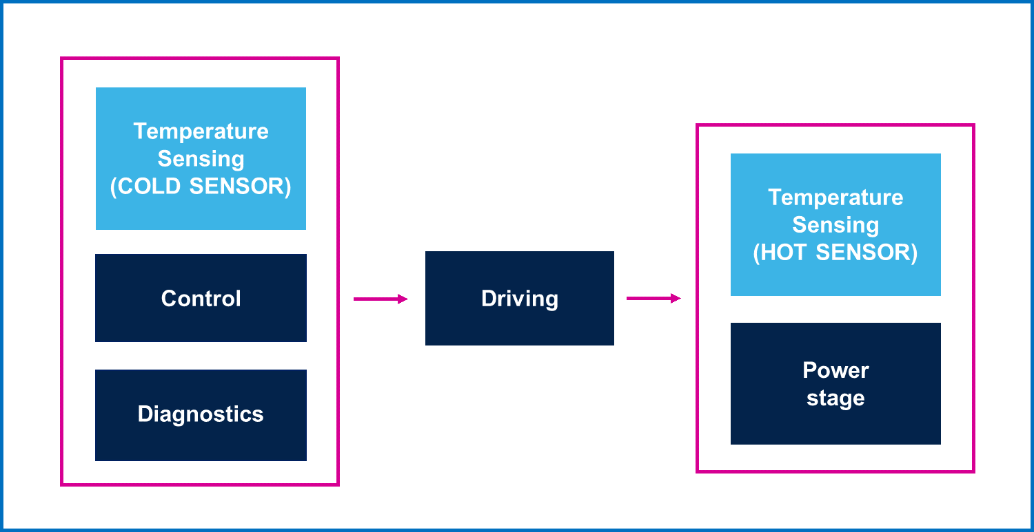 Fig. 1 Simplified block diagram of a smart switch with different temperature sensors.
The temperature sensors are implemented using polysilicon diodes thanks to their linear temperature coefficient across operating temperatures. The cold sensor is positioned in the cold zone of the driver near the controller, while the hot sensor is placed in the power stage area, which is the hottest zone in the driver.
Using this double-sensor technique enables the driver’s temperature increase to be limited since the thermal protection is triggered when the lowest temperature value between the over-temperature threshold and a dynamic temperature level between the sensors is reached. Once removed the overtemperature fault, the smart switch can be reactivated when the temperature decreases to a fixed value.
This significantly helps to reduce thermal fatigue in terms of thermo-mechanical stress on the switch, which can accumulate over time and lead to degradation and reduced reliability.
Thermal Mapping
Along with simulation and prevention procedures, infrared (IR) thermography is a valuable technique to obtain detailed thermal maps of the driver, which provide a comprehensive understanding of the heat distribution within the integrated circuit, highlighting any potential hazard.
To assess the effectiveness of intelligent protections in harsh automotive applications, the heat distribution within the driver has to be analyzed under challenging short-circuit conditions with two different scenarios:
- Terminal Short-Circuit (TSC);
- Load Short-Circuit (LSC).
The terminal short-circuit condition occurs when a low resistance connection between the terminals of a component or device is present, as shown in Fig. 2.
 Fig. 2 Testing circuit for temperature measurement under TSC.
On the other hand, a load short-circuit condition arises when there is an inductive path between the load and the power source, leading to a sudden surge in current flow (Fig. 3).
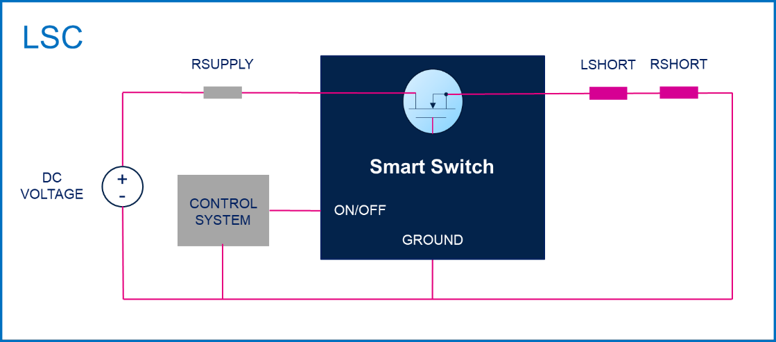 Fig. 3 Testing circuit for temperature measurement under LSC.
The following test conditions are considered:
- Tamb = 25 °C
- Vbat = 14 V
- Ton = 1 ms for mapping
- Ton = 300 ms for temperature acquisition of thermal sensors and hot spots
- TSC condition: RSUPPLY = 10 mΩ, RSHORT = 10 mΩ
- LSC condition: RSUPPLY = 10 mΩ, LSHORT = 5 µH, RSHORT = 100 mΩ
where Tamb is the ambient temperature
Vbat the DC battery voltage
Ton the time duration of the short-circuit event
RSUPPLY the resistance of the battery
RSHORT the short-circuit resistance
LSHORT the short-circuit inductance.
In order to generate a temperature map, the IR camera sensor is utilized to capture the infrared emissions at each location, which are then converted into temperature values. To ensure the conversion accuracy from specific colors to defined temperature values, a calibration process is essential. This process involves comparing the different colors obtained from the sensor with known temperature values, which can be obtained through specific thermal sensitive parameters and their trend versus temperature increase. By analyzing these parameters, the calibration process can ensure that the temperature map accurately reflects the temperature distribution in the area being scanned.
To calibrate the IR camera sensor, the forward voltage (VF) of the MOSFET’s body drain diode is chosen due to its linear dependence on temperature. However, a pre-calibration of the diode is necessary to accurately determine its temperature coefficient. This is achieved by measuring the VF voltage at a constant forward current (IF) while varying the temperature from 25°C to 100°C. To prevent any temperature rise caused by the current and its associated power dissipation, the IF value is selected within the range of 10mA to 20mA.
The VF values collected at different temperatures can be used to perform a linear interpolation and mathematical fitting to obtain the temperature coefficient of the diode, as shown in Fig. 4.
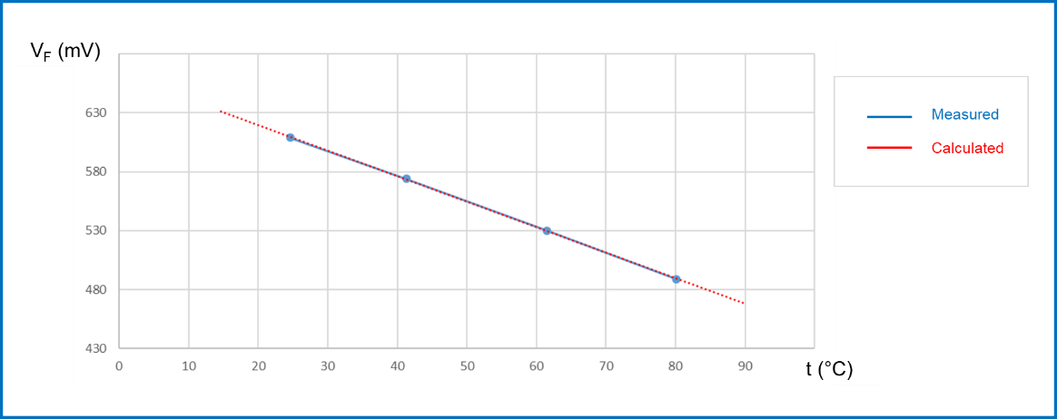 Fig. 4 Pre-calibration of MOSFET’s body drain diode.
Calculations are made through the following equation (1):
Dt = DVF /K (1)
where:
Dt is the temperature variation;
DVF the forward voltage variation;
K is the temperature coefficient of the diode.
The temperature map is created by acquiring each temperature point through an IR camera sensor at 1ms intervals. Once all the die points are acquired (which takes around 3000 seconds), a specialized software generates the map, which depicts the temperature of each point based on the minimum spatial resolution of the IR sensor. By overlaying the thermal map onto the row silicon die picture, it is possible to identify the hottest points in the active area and determine their coordinates while the current flows through the device.
As an example, the thermal maps for the dual-channel VND9012AJ smart switch are depicted in Fig. 5 under TSC conditions.
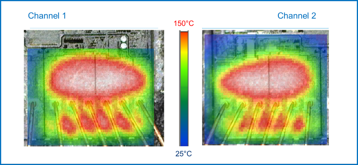 Fig. 5- Thermal maps for VND9012AJ channels under TSC condition.
The graphical representation of temperature distribution across the driver’s channels, depicted through varying colors within the temperature range of 25°C to 150°C, serves as a crucial aid in detecting any regions experiencing excessive heat and ensuring the driver’s safe temperature operation. The provision of thermal maps for each channel under diverse operating conditions enables the tests to authenticate the driver’s reliable functioning without surpassing its maximum temperature threshold.
In order to locate the hot spots and monitor the temperature evolution for both hot and cold sensors, and subsequently validate the efficacy of the thermal shutdown mechanism, a longer short-circuit duration of 300ms is taken into account.
The temperature variations observed in VND9012AJ while undergoing TSC are displayed in Fig. 6.
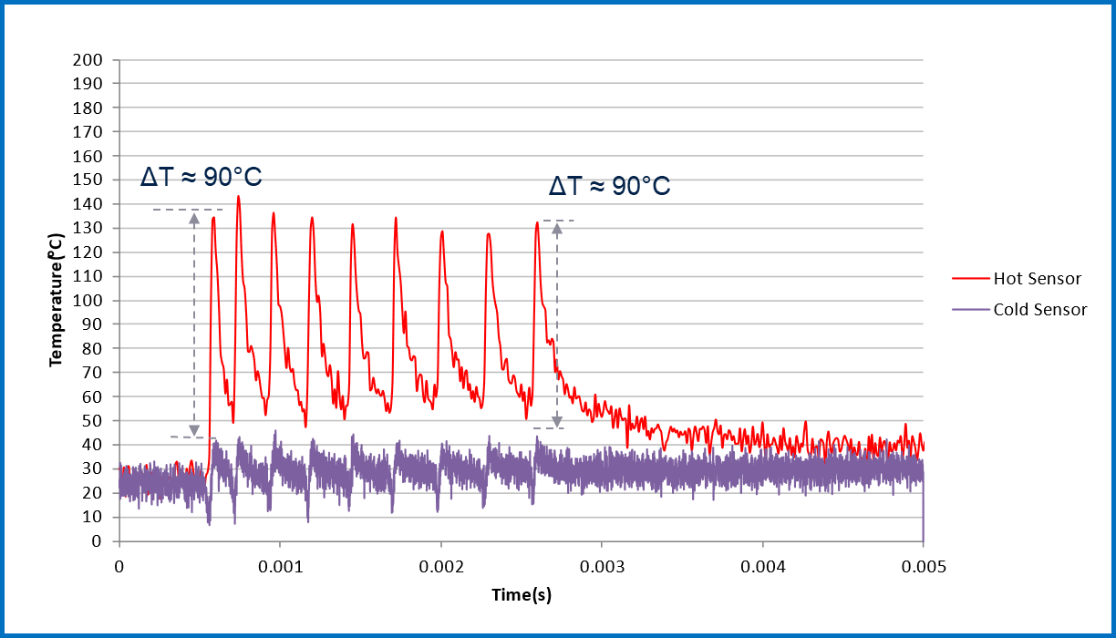 Fig. 6- Temperature variations for both sensors under TSC condition.
The graph indicates the presence of hot spots in both channels of VND9012AJ as detected by the hot sensors, and the maximum temperature of these hot spots is in the range of 150 °C.
The thermal maps for VND9012AJ under LSC conditions are presented in Fig. 7.
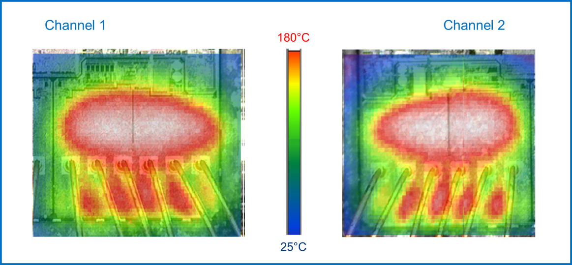 Fig. 7- Thermal maps for VND9012AJ channels under LSC condition.
The temperature variations observed in VND9012AJ while undergoing LSC are displayed in Fig. 8.
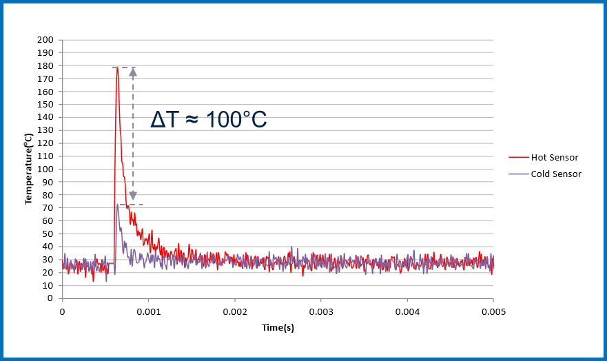 Fig. 8 Temperature variations for both sensors under LSC condition.
Both conditions trigger the thermal protection mechanism, causing the current to be limited to a safe level.
Conclusions
Valuable insights into the design and operation of the smart switch have been obtained through experimental results, particularly regarding current distribution and thermal protection mechanisms. It is essential to maintain a well-balanced behaviour of all channels to create an intelligent driver that improves safety and reliability in automotive systems. The use of IR thermography enables a precise and comprehensive analysis of temperature distribution, which enhances the smart switch’s thermal sensing and protection system. In demanding automotive environments, swift activation of these protections is crucial to detect overheating and prevent any potential harm to the device or system.
References
[1] P. Meckler and F. Gerdinand, “High-speed thermography of fast dynamic processes on electronic switching devices”, 26th International Conference on Electrical Contacts (ICEC 2012), 2012.
[2] X. Zhou and T. Schoepf, “Detection and formation process of overheated electrical joints due to faulty connections”, 26th International Conference on Electrical Contacts (ICEC 2012), 2012.
[3] T. Israel, M. Gatzsche, S. Schlegel, S. Großmann, T. Kufner, G. Freudiger, “The impact of short circuits on contact elements in high power applications”, IEEE Holm Conference on Electrical Contacts, 2017.
[4] Y. Lozanov, “Assessment of the technical condition of electric contact joints using thermography”, 17th Conference on Electrical Machines, Drives and Power Systems (ELMA), 2021.
[5] M. Bonarrigo, G. Gambino, F. Scrimizzi, “Intelligent power switches augment vehicle performance and comfort”, Power Electronics News, Oct. 10, 2023.
The post Balancing Currents for Optimal Performance in Automotive Smart Drivers appeared first on ELE Times.
Rohde & Schwarz expands footprint in India by opening a futuristic facility in Delhi
Rohde & Schwarz, the technology leader inaugurates a state-of-the-art facility in New Delhi, as part of the company’s long-term vision for India. Rohde & Schwarz, is making significant strides in India with recent expansions and strategic initiatives, from fortifying its facilities to venturing direct entry into Defence projects. With a global to-local approach, Rohde & Schwarz emphasises increasing local value additions by production, Research & Development, Application Development, customization for India-specific needs, and system integration, all well fitting into the ‘Make in India’ initiative.
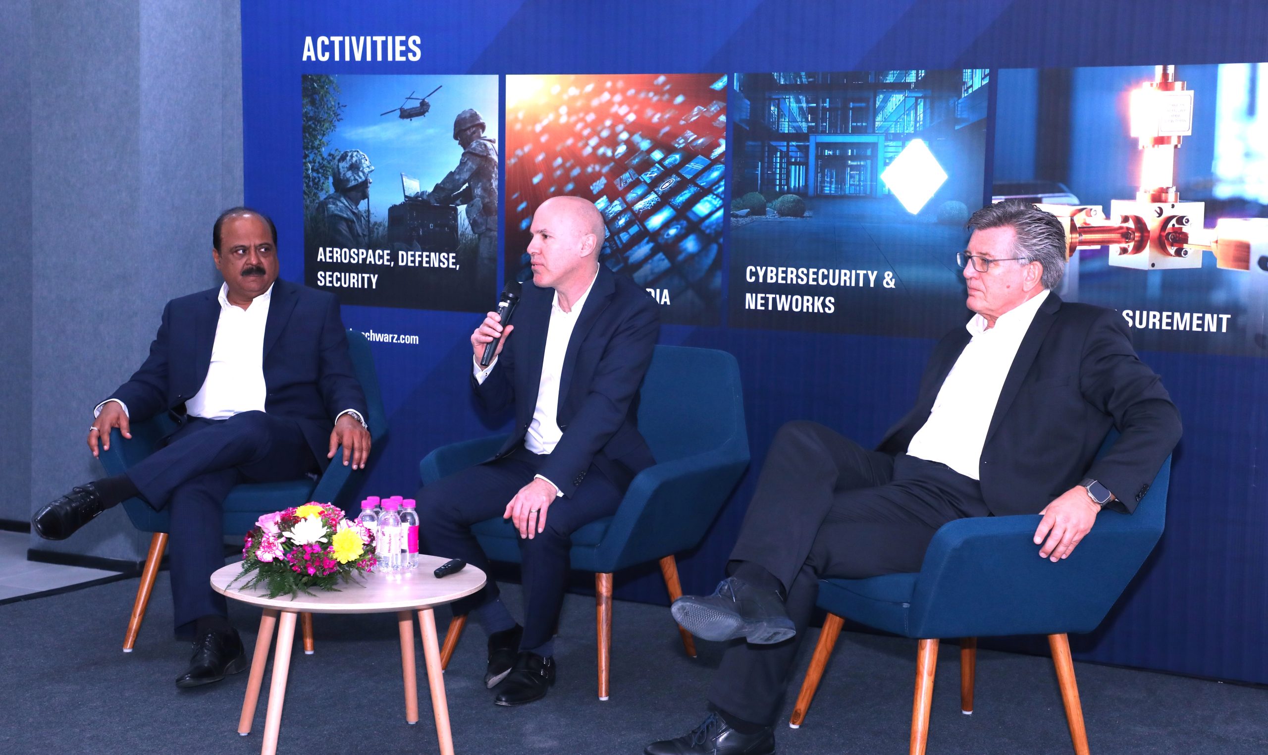 From Left to Right: Yatish Mohan, Managing Director of Rohde & Schwarz India
Dr. Alexander Orellano, Executive Vice President, Technology Systems of Rohde & Schwarz, Ralf Watamaniuk, Vice President of Sales & Marketing, Rohde & Schwarz GmbH & Co. KG, addressing media during the grand opening of its new facility located at Mohan Cooperative Industrial Estate, in New Delhi
Rohde & Schwarz India, the Indian subsidiary of the German-based, global technology company Rohde & Schwarz, celebrated the grand opening of its new facility located at Mohan Cooperative Industrial Estate, in New Delhi.
While inaugurating the new facility, Dr. Alexander Orellano, Executive Vice President, Technology Systems of Rohde & Schwarz, said: “We are proud to expand our presence in New Delhi. The new facility marks a significant step forward in the company’s commitment to enhancing local production, software development, system integration, and assembly in line with the Indian government’s objective of ‘Make in India’. For Rohde & Schwarz, India is not merely a growth market but a vital component of our global strategy”.
Yatish Mohan, Managing Director of Rohde & Schwarz India, expressed his pride in the company’s contribution to India’s defense, aviation, and surveillance capabilities, stating, “As a leading ecosystem partner in the Indian technology industry, Rohde & Schwarz India is proud to contribute to the nation’s defense, aviation, and surveillance capabilities. Our focus on innovation, collaboration, and local value addition underscores our commitment to driving positive change and shaping the future of India’s technological landscape. The new facility aims to further enhance these capabilities and serve as a center of competence for surveillance solutions”.
Rohde & Schwarz India has been a pivotal ecosystem partner in India’s technology industry, catering to critical sectors such as defense, civil aviation, and surveillance. The company plays a significant role in providing cutting-edge technological solutions and services to key sectors like defense, civil aviation, surveillance, and more. Highlighting Rohde & Schwarz India’s successful implementations, such as the deployment of state-of-the-art Milli Meter Wave Full Body Scanners at Bengaluru airport, the company has been at the forefront of innovation in defense and aviation, developing advanced systems and solutions tailored to the unique requirements of these sectors.
The post Rohde & Schwarz expands footprint in India by opening a futuristic facility in Delhi appeared first on ELE Times.
Infineon expands its leading market position in automotive semiconductors – World market leader in automotive MCUs for the first time
Infineon Technologies AG continued to expand its leading market position in automotive semiconductors in 2023. According to the latest research by TechInsights[1], the global automotive semiconductor market grew by 16.5 per cent in 2023, reaching a new record size of US$69.2 billion. Infineon’s overall market share increased by one percentage point, from nearly 13 per cent in 2022 to about 14 per cent in 2023, solidifying the company’s position as the global leader in the automotive semiconductor market. Infineon’s semiconductors are essential in serving all automotive key applications like driver assist and safety systems, powertrain and battery management, comfort, infotainment and security.
According to TechInsights, Infineon has increased its market share in all regions and remained market leader in South Korea and China. In addition, Infineon has made significant gains in the Japanese automotive semiconductor market. Infineon has strengthened its strong European presence as the second-largest player, as well as its top-three position in North America.
 Peter Schiefer, President of the Automotive Division at Infineon
“We are very proud that we have expanded our position as the leading automotive semiconductor supplier. This great success is based on our product innovation and system competence that add value to our customers’ solutions,” said Peter Schiefer, President of the Automotive Division at Infineon. “We also see this achievement as motivation, since our automotive semiconductors are the basis for the future of mobility, making cars clean, safe and smart.”
“Infineon maintained the top spot in the TechInsights automotive semiconductor 2023 vendor market share rankings with nearly 14 per cent market share,” said Asif Anwar, Executive Director of Automotive End Market Research at TechInsights. “The company’s automotive semiconductor revenues grew over 26 per cent year-on-year, allowing the company to stretch its lead over its second and third place rivals by four percentage points.”
Global number one in automotive microcontrollers
A major driver of Infineon’s performance was strong automotive microcontroller (MCU) sales. For the first time, Infineon has reached the world’s number one position in this market. The company’s sales in the automotive microcontroller segment increased by nearly 44 per cent compared to 2022, resulting in a 2023 market share of about 29 per cent worldwide.
Microcontrollers are key components in the automotive industry, controlling and monitoring a wide variety of systems in the automobile such as electric powertrain, electric-electronic (E/E) architecture, advanced driver assistance systems (ADAS) and automated driving, radar and chassis. Infineon’s AURIX flagship microcontroller family and the TRAVEO microcontroller family are the main contributors to this success, driving the transition in the automotive industry towards autonomous, connected and electrified vehicles. The families combine power and performance enhancements with the latest trends in the fields of virtualization, AI-based modeling, functional safety, cybersecurity and network functions. They are paving the way for new E/E architectures as well as the next generation of software-defined vehicles.
[1] TechInsights: Automotive Semiconductor Vendor Market Shares. April 2024
The post Infineon expands its leading market position in automotive semiconductors – World market leader in automotive MCUs for the first time appeared first on ELE Times.
Infineon and Amkor deepen partnership and strengthen European supply chain for semiconductor solutions
Infineon Technologies AG, a leader in power systems and IoT, is strengthening its outsourced backend manufacturing footprint in Europe and announced a multi-year partnership with Amkor Technology, Inc., a leading provider of semiconductor packaging and test services. Both companies have agreed on operating a dedicated packaging and test centre at Amkor’s manufacturing site in Porto. Operations are expected to commence in the first half of 2025.
With this long-term agreement, Infineon and Amkor further strengthen their partnership, extending the classical Outsourced Semiconductor Assembly and Test (OSAT) business model. Amkor will expand its facilities in Porto and run the production line, providing dedicated clean room space, and Infineon will provide an onsite team with engineering and development support. The cooperation further strengthens the European semiconductor supply chain and contributes to making it more resilient – especially for automotive customers. It complements Infineon’s already diversified manufacturing footprint, balancing in-house and outsourced production capabilities.
”We are pleased to further deepen our partnership with Amkor and will contribute with our engineering and development expertise,” said Alexander Gorski, Executive Vice President and responsible for Infineon’s global Backend Operations. ”Infineon and Amkor are jointly increasing geographical resilience and supply security for our customers. Together, we are strengthening Europe’s importance as a location for semiconductor manufacturing. For 20 years, Infineon has been successfully operating a large service centre in Porto, now with more than 600 employees. With the joint manufacturing centre, we are becoming even more deeply rooted in Portugal’s excellent semiconductor ecosystem. We are looking forward to further increasing our footprint in Portugal.”
“Amkor is proud to expand our partnership with Infineon,” said Giel Rutten, Amkor’s president and chief executive officer. “We continue to invest in our Porto manufacturing site, expanding capacity as well as broadening our Advanced packaging and test technology portfolio. This collaboration represents another milestone for both companies in enhancing supply chain resiliency for advanced products supporting Automotive & Industrial end markets.”
The post Infineon and Amkor deepen partnership and strengthen European supply chain for semiconductor solutions appeared first on ELE Times.
Arrow Electronics Launches Intelligent Vision Ecosystem
CENTENNIAL, Colo.–(BUSINESS WIRE)– Arrow Electronics, Inc. is utilizing the onsemi Imager Access System (IAS) module standard for developing intelligent vision solutions for use in robotics, machine vision, commercial cameras and other uses.
The solution reduces the design complexities that are common with designing a product that utilizes image sensors. Part of that complexity is there is no standardization of the hardware interfaces of the different technology blocks. This is where the onsemi IAS module standard comes in and is adopted throughout the ecosystem.
Working with Appletec, Arrow developed the newest IAS module, AP-VISION-AR0830-83, that utilizes the latest generation of onsemi image sensors.
“The onsemi Hyperlux LP family of sensors set a new industry benchmark for ultra-low power sensor design. Combined with a small form factor, purpose-oriented features and best-in-class imaging, Hyperlux LP will be a fixture for smart home, office, and robotics for years to come,” said Stephen Harris, senior director of marketing for onsemi’s Industrial and Commercial Sensing Division. “onsemi is now able to bring the newest high-performance, feature-rich 4K sensor in the Hyperlux family, AR0830, to market with Arrow’s IAS module, allowing our customers to reduce camera development efforts significantly with best-in-class module design.”
This new module joins the existing portfolio of IAS modules offered by Arrow and Appletec.
Arrow worked with its company, eInfochips, and onsemi to develop drivers that enable the Appletec IAS modules to work with leading embedded processors.
“eInfochips has extensive experience in developing end-to-end vision solutions. This includes hardware design, image sensor integration and tuning, image processing, image driver development, low latency streaming and AI Inferencing on edge/cloud,” said Gaurav Patel, vice president and general manager of product engineering services for eInfochips. “Companies rely on eInfochips to deliver innovative vision solutions and accelerate and de-risk design cycles.”
The post Arrow Electronics Launches Intelligent Vision Ecosystem appeared first on ELE Times.
Infineon expands automotive offering with programmable high voltage PSoC 4 HVMS family for touch-enabled HMI and other smart sensing applications
Munich, Germany – In the automotive industry, security and functional safety are playing an increasingly important role even in low-end microcontroller applications. At the same time, vehicle manufacturers are replacing mechanical buttons by touch enabled surfaces that blend into a clean cockpit or steering wheel. As a result, there are strong space limitations for the electronic circuits, and a demand for highly integrated ICs with a small form factor. To tackle these challenges, Infineon Technologies AG introduces the PSoC 4 HVMS family of automotive microcontrollers, integrating high voltage features (12 V-regulator and LIN/CXPI-transceiver) in combination with advanced analog features (CAPSENSE, Inductive sensing), ISO26262 compliant and ISO21434 ready.
Target applications include touch-enabled automotive HMIs (Human Machine Interfaces) with touch buttons, sliders, and touchpads for controlling HVAC, interior lighting, power windows/sunroofs or in door handles. In steering wheels, the PSoC 4 HVMS is used for touch sensing as well as safety-critical hands-off detection. The latest generation CAPSENSE module also supports proximity detection for occupant detection or foot kick control. In addition to HMI applications, the PSoC 4 HVMS is also used in generic sensing applications (such as liquid level sensing, Wheatstone bridge sensing, etc.) or in simple actuators such as a PTC heater or interior/exterior lighting.
The PSoC 4 HVMS family is AEC-Q100 qualified and offered in small footprint QFN packages with wettable flanks. The ICs offer scalability and pin compatibility across devices. ISO26262 ASIL-B compliance ensures safe operation at temperatures up to 125°C. The family is based on ARM Cortex-M0+ processors with up to 128 KB of embedded flash and 16 KB of SRAM. The microcontrollers can be powered directly from a 12 V battery and include LIN and CXPI PHY. For capacitive sensing applications, the device supports the latest 5th generation CAPSENSE technology with eight times better SNR than the previous generation, support for high parasitic capacitance up to 3000 pF and support for overlays up to 18 mm. Additional analog integration includes a 12-bit SAR ADC, up to two operational amplifiers and low power comparators.
The microcontroller family is accompanied by comprehensive software support including Automotive Peripheral Driver Library (AutoPDL), Automotive Middleware Library for CAPSENSE, and the Safety Library (SafeTlib) for Automotive PDL, accelerating the time-to-market by significantly reducing customer development time. The software package is developed in adherence to automotive software development processes, including ASPICE, MISRA2012 AMD1, and CERTC coding standards, and guarantees industry-leading reliability and compliance. The PSoC 4 HVMS software package is ISO26262 compliant and developed as a Safety Element out of Context (SEooC) for applications with safety targets up to ASIL-B. The ModusToolbox software development platform will be additionally available soon.
AvailabilitySamples of the PSoC4 HVMS controllers are available for both the 64 K and 128 K families. The series is expected to go into production in 2024. More information is available at https://www.infineon.com/psochv.
Infineon at Embedded WorldEmbedded World will take place in Nuremberg, Germany, from 9 to 11 April, 2024. Infineon will present its products and solutions for decarbonization and digitalization in hall 4A, booth #138 and virtually. Company representatives will also hold several TechTalks as well as presentations at the accompanying Embedded World Conference, followed by discussions with the speakers. If you are interested in interviewing an expert at the show, please email media.relations@infineon.com, Industry analysts interested in a briefing can email MarketResearch.Relations@infineon.com. Information about the Embedded World show highlights is available at www.infineon.com/embeddedworld.
The post Infineon expands automotive offering with programmable high voltage PSoC 4 HVMS family for touch-enabled HMI and other smart sensing applications appeared first on ELE Times.
Infineon introduces the XENSIV Sensor Shield for Arduino with Infineon and Sensirion sensors for Smart Home applications
Infineon Technologies has announced the XENSIV Sensor Shield for Arduino, a versatile tool designed for evaluating smart sensor systems in smart home and diverse consumer applications. This innovative shield incorporates a wide range of sensors from Infineon’s portfolio along with Sensirion’s SHT35 humidity and temperature sensor which streamlines its capabilities and enhances the design journey of Infineon’s customers. This shield empowers design engineers to evaluate, prototype and develop sensor-based applications faster by fully leveraging Infineon microcontrollers, wireless connectivity and security chips. As a result, it serves as an exceptional platform for enabling accelerated innovation in sensor powered solutions.
“We are very pleased to be teaming up with Sensirion“, said Philipp von Schierstädt, EVP & CSO Consumer, Computing & Communication at Infineon. “Together we can expand our product range and ease the work of application designers.” With the new shield customers addressing smart home applications such as HVAC will have the opportunity to develop within Infineon’s ecosystem and gain access to additional sensors beyond the company’s consumer sensor portfolio of microphones, pressure sensors, CO2 and radar sensors.
The XENSIV Sensor Shield for Arduino enables seamless hardware interoperability between multiple Infineon MCUs and sensors as a fully integrated development platform. The featured sensors include XENSIV 60 GHz Radar, PAS CO2, Pressure, PDM Microphones, IMU accelerometer and the Sensirion SHT35 humidity and temperature sensor. The shield seamlessly integrates with Infineon’s microcontroller kits and provides convenient access via an Arduino Uno connector. As part of Infineon’s ongoing commitment to deliver comprehensive system solutions, the shield is specifically designed and optimized to work with targeted MCUs in the Infineon lineup such as PSoC 6, AIROC Bluetooth SoCs and Wi-Fi MCUs.
To further accelerate time-to-market and improve the customer experience while working within Infineon’s ecosystem, the XENSIV Sensor Shield for Arduino is fully enabled to work with Infineon’s ModusToolbox software development platform for simplified software integration. ModusToolbox provides a comprehensive development environment: a unified platform with all tools and resources needed for embedded system development. Included code generation and configuration wizards automate repetitive tasks and simplify complex configurations. The ModusToolbox development ecosystem is designed to scale with project requirements and adapt to changing needs, providing developers with essential libraries and code examples necessary for rapidly prototyping a variety of applications.
Designers can also leverage the sensors of the XENSIV Sensor Shield for Arduino in Machine Learning use cases, utilizing Infineon microcontrollers, ModusToolbox and Imagimob Machine Learning together with Infineon’s broad sensor capabilities and Sensirion’s temperature and humidity sensor.
AvailabilityThe new XENSIV Sensor Shield for Arduino will be available in the third quarter of 2024. Infineon will be showcasing the shield at Embedded World in Nuremberg.
Infineon at Embedded WorldEmbedded World will take place in Nuremberg, Germany, from 9 to 11 April 2024. Infineon will present its products and solutions for decarbonization and digitalization in hall 4A, booth #138 and virtually. Company representatives will also hold several TechTalks as well as presentations at the accompanying Embedded World Conference, followed by discussions with the speakers. If you are interested in interviewing an expert at the show, please email media.relations@infineon.com. Industry analysts interested in a briefing can email MarketResearch.Relations@infineon.com. Information about the Embedded World show highlights is available at www.infineon.com/embedded-world.
The post Infineon introduces the XENSIV Sensor Shield for Arduino with Infineon and Sensirion sensors for Smart Home applications appeared first on ELE Times.
Cadence’s Design and Software Strategy Aces Electronic and Technology Marvels
Cadence Design Systems is a tech-savvy organisation building the most intricate and in-demand electronic system designs, actively developing critical components in segments of IC design, verification, Digital design and signoff, Multiphysics analysis, PCB design, molecular simulation etc., and engineering marvels at the helm of technologies like AI, 3D-IC, mixed-signal, photonics, computational fluid dynamics etc. Also as an industry giant, the team caters to areas like 5G systems and subsystems, aerospace and defense, automotive, hyperscale computing, and life sciences.
 Ms Madhavi Rao, Field Marketing Group Director EMEAI at Cadence Design Systems
Rashi Bajpai, Sub-Editor at ELE Times spoke with Ms Madhavi Rao, Field Marketing Group Director EMEAI at Cadence Design Systems on the various technologies Cadence is currently working on and their expertise in the field.
This is an excerpt from the conversation.
ELE Times: Brief us on Cadence’s Intelligent System Design strategy and the road ahead.
Madhavi Rao: Electronics is pervasive in every aspect of life and business, from consumer applications to automotive to cloud computing, and everything in between. As a result, the need for seamless integration, top performance, low power, small form factor, thermal considerations, and advanced features – to name a few – have become crucial.
To address these complexities, semiconductor and systems companies require comprehensive solutions encompass chips, IP, PCB & packaging, and system design solutions. Cadence has addressed this change in dynamics through its Intelligent System Design strategy, which includes the following key elements:
Design Excellence: Cadence offers an optimized EDA toolkit comprising tools and IP for semiconductor, package, and PCB design, with scalable distributed computing capabilities in the cloud. This allows customers to solve a broad range of large complex challenges.
System Innovation: Expanding beyond EDA to facilitate early software development and to optimize the entire system for various critical factors such as security, responsiveness, power efficiency, electromagnetics, thermal performance, Multiphysics considerations, and more.
Pervasive intelligence: To enable the creation of sophisticated systems, machine learning (ML) technologies have been incorporated into design tools and in workflows.
ELE Times: Cadence Design Systems is well-renowned in the electronics industry for its consumer-centric software used in designing chips and electronic systems. What in your opinion are the latest and upcoming trends that will drive the market of chip designing and the overall semiconductor industry in India?
Madhavi Rao: Over the years, semiconductor companies in India have played a crucial role in providing design services and contributing to research and development efforts for global companies. In the last few years, recognizing the strategic importance of semiconductor manufacturing and design for the country’s economic growth and technological advancement, there has been a greater push from the Government of India to make India self-reliant in electronics, and a semiconductor hub for the world. The government initiatives to attract investment and promote indigenous semiconductor development have created a positive atmosphere for the growth of the semiconductor industry.
Focus on Domestic Manufacturing and Investment in Fab Facilities
Countries the world over, including India, have been focusing on regional self-sufficiency in semiconductor manufacturing.
Indian policymakers and industry stakeholders have expedited their efforts to establish India as a hub for semiconductor manufacturing and supply chains, with various incentives and schemes. Of late we have seen a significant amount of investment from global players to set up fab facilities in India. These fab facilities are expected to catalyze the growth and development of the Indian semiconductor industry, driving innovation, creating jobs, enhancing supply chain resilience, and positioning India as a competitive player in the global semiconductor landscape.
Collaborations are critical in developing the local manufacturing ecosystem. Several international semiconductor companies are investing in India’s semiconductor ecosystem through collaborations, which provide expertise, technology transfer, and investment capital, fuelling the growth of the semiconductor industry in India.
Leveraging the opportunity of the huge domestic market
India’s consumer electronics market is growing exponentially, thanks to factors such as urbanization, increasing disposable income, and government initiatives such as Digital India and Make in India. This growth has led to a significant increase in demand for semiconductor chips. In addition, there are a multitude of opportunities for “designing for India” – creating electronic products that cater to India’s unique needs. This presents a huge opportunity for local entrepreneurs to innovate.
Design and Innovation Ecosystem
Globally, India is recognized as a chip design powerhouse. According to IESA, 20% of the world’s chip designers work out of India. Initiatives like the India Semiconductor Mission strengthen the design and innovation ecosystem, which will be crucial for developing more intellectual property (IP) and design startups in India.
ELE Times: How is Cadence addressing the requirements of 3D-IC design in several areas of implementation, and further help us understand the role of 3D IC technology in strengthening the semiconductor ecosystem in India?
Madhavi Rao: 3D-IC (Three-Dimensional Integrated Circuit) is a technology where multiple layers of integrated circuits (ICs) are stacked on top of each other rather than placed on a single silicon wafer. Compared to traditional two-dimensional ICs, this vertical stacking optimises space utilisation, enhances performance, and improves functionality.
Cadence has a 3D-IC solution that provides 3D design planning, implementation, and system analysis in a single, unified cockpit. It enables hardware and software co-verification and full-system power analysis using emulation and prototyping and chiplet-based PHY IP for connectivity with power, performance, and area (PPA) optimized for latency, bandwidth, and power. The solution also offers co-design capabilities with custom analog design and board design, integrated circuit (IC) signoff extraction, static timing analysis (STA) and signoff with signal and power integrity (SI/PI), electromagnetic interference (EMI), and thermal analysis.
Similar to the evolution of commercial third-party IP, which led to the development of a thriving market for soft and hard IP, the 3D-IC chiplet landscape offers significant opportunities for growth and the emergence of a market for commercial third-party chiplets. This evolution is expected to unfold over the coming years, requiring the definition and enforcement of standards to facilitate seamless integration. This could present a unique opportunity for India to take the lead.
ELE Times: In light of your recent collaboration with MeitY to provide EDA tools for free to companies looking to set up their chip design centres in India under the DLI scheme, how involved is Cadence in promoting the start-up ecosystem in India in the electronics and technology sector?
Madhavi Rao: For more than 20 years, Cadence has been closely involved in workforce development. From the establishment of the government’s Specialized Manpower Development Program (SMDP) Phases I and II, we have been actively taking part in the program. Currently we are working with MeitY for the Chips to Startup Program, aimed at training engineers in VLSI design.
Cadence is proud to be working closely with MeitY to realize the ambition of developing a pool of 85,000 trained engineers by 2027.
Over 350 academic institutions are enrolled in the The Cadence Academic Network, where students have access to Cadence’s world-class technology. In addition, Cadence has been actively engaged with various training institutes that are involved with upskilling, reskilling, and acquiring lateral skills to meet the industry’s demands.
Cadence has been working together with startups to nurture the semiconductor industry’s growth in India by empowering them with access to cutting-edge tools, technologies, and expertise since 2006.
Specific engagements of Cadence’s in promoting startups in India consist of:
- Providing tailored business models for startups.
- Cadence has partnered with startup incubators like FABCi – IIT Hyderabad and Electropreneur Park in Delhi and Bhubaneswar to provide software, guidance, and mentorship to semiconductor and electronics startups.
- Cadence also has strong ties with academic institutions across India, fostering a culture of innovation. Startups benefit from this ecosystem through collaborations on research projects, access to talent, and opportunities for academia-industry partnerships.
Through events, conferences, and customer forums, Cadence facilitates networking opportunities for startups.
ELE Times: With over 30% of its workforce in India, Cadence handles major R&D projects and product development from India. Shed some light on your global R&D goals and how India is helping global operations for Cadence.
Madhavi Rao: Cadence is one of the early MNCs to enter India. We have had a presence in India for over 35 years, with a workforce across Noida, Bengaluru, Ahmedabad, Hyderabad and Pune. 30% of our global employees are based in India.
Cadence offers end-to-end tools for chip and system design, including IP and hardware. Our R&D teams in India collaborate with R&D teams across the world on our product portfolios in digital design and signoff, functional verification, formal verification, hardware and prototyping, IP, custom and mixed-signal design, PCB and IC Packaging design and System design.
ELE Times: Give some insights into Cadence’s Millennium M1 platform, its key features, benefits, and applications.
Madhavi Rao: Designing mechanical systems for new levels of performance and efficiency has become a key priority in the automotive, aerospace and defense (A&D), energy, and turbomachinery industries. To optimize performance and reduce greenhouse gases, automotive designers are focused on improving fuel efficiency, reducing drag and noise, and extending electric vehicle range. Increasing efficiency, reducing carbon emissions and reducing maintenance frequency are top of mind for A&D and turbomachinery design engineers. Advances in multiphysics simulation technology are critical to achieving these goals. Cadence Millennium Platform addresses these needs.
Cadence Millennium Enterprise Multiphysics Platform is the industry’s first hardware/software accelerated digital twin solution for multiphysics system design and analysis. Targeted at one of the biggest opportunities for greater performance and efficiency, the first-generation Cadence Millennium M1 accelerates high-fidelity computational fluid dynamics (CFD) simulations. This turnkey solution includes graphics processing units (GPUs) from leading providers, extremely fast interconnections and an enhanced Cadence high-fidelity CFD software stack optimized for GPU acceleration and generative AI. Millennium M1 instances can be fused into a unified cluster, enabling customers to achieve an unprecedented same-day turnaround time and near-linear scalability when simulating complex mechanical systems.
Key highlights and benefits include:
- Performance: Combines best-in-class GPU-resident CFD solvers with dedicated GPU hardware to provide supercomputer-equivalent throughput per GPU of up to 1000 CPU cores
- Efficiency: Reduces turnaround time from weeks to hours with 20X better energy efficiency compared to its CPU equivalent
- Accuracy: Leverages Cadence Fidelity
 CFD solvers to provide unmatched accuracy to address complex simulation challenges
 - High-Performance Computing: Built with an extensible architecture and massively scalable Fidelity solvers to provide near-linear scalability on multiple GPU nodes
- AI Digital Twin: Rapid generation of high-quality multiphysics data enables generative AI to create fast and reliable digital twin visualizations of the optimal system design solution
- Turnkey Solution: The industry’s first solution that couples GPU compute with modern and scalable CFD solvers, providing an optimized environment for accelerated CFD and multidisciplinary design and optimization
- Flexibility: Available with GPUs from leading vendors, in the cloud with minimum 8 GPU configurations, or on-premises with a minimum 32 GPU configurations—providing a flexible and scalable solution to fit each customer’s deployment needs.
The post Cadence’s Design and Software Strategy Aces Electronic and Technology Marvels appeared first on ELE Times.
Pages

