
ELE Times

Cadence’s Design and Software Strategy Aces Electronic and Technology Marvels
Cadence Design Systems is a tech-savvy organisation building the most intricate and in-demand electronic system designs, actively developing critical components in segments of IC design, verification, Digital design and signoff, Multiphysics analysis, PCB design, molecular simulation etc., and engineering marvels at the helm of technologies like AI, 3D-IC, mixed-signal, photonics, computational fluid dynamics etc. Also as an industry giant, the team caters to areas like 5G systems and subsystems, aerospace and defense, automotive, hyperscale computing, and life sciences.
 Ms Madhavi Rao, Field Marketing Group Director EMEAI at Cadence Design Systems
Rashi Bajpai, Sub-Editor at ELE Times spoke with Ms Madhavi Rao, Field Marketing Group Director EMEAI at Cadence Design Systems on the various technologies Cadence is currently working on and their expertise in the field.
This is an excerpt from the conversation.
ELE Times: Brief us on Cadence’s Intelligent System Design strategy and the road ahead.
Madhavi Rao: Electronics is pervasive in every aspect of life and business, from consumer applications to automotive to cloud computing, and everything in between. As a result, the need for seamless integration, top performance, low power, small form factor, thermal considerations, and advanced features – to name a few – have become crucial.
To address these complexities, semiconductor and systems companies require comprehensive solutions encompass chips, IP, PCB & packaging, and system design solutions. Cadence has addressed this change in dynamics through its Intelligent System Design strategy, which includes the following key elements:
Design Excellence: Cadence offers an optimized EDA toolkit comprising tools and IP for semiconductor, package, and PCB design, with scalable distributed computing capabilities in the cloud. This allows customers to solve a broad range of large complex challenges.
System Innovation: Expanding beyond EDA to facilitate early software development and to optimize the entire system for various critical factors such as security, responsiveness, power efficiency, electromagnetics, thermal performance, Multiphysics considerations, and more.
Pervasive intelligence: To enable the creation of sophisticated systems, machine learning (ML) technologies have been incorporated into design tools and in workflows.
ELE Times: Cadence Design Systems is well-renowned in the electronics industry for its consumer-centric software used in designing chips and electronic systems. What in your opinion are the latest and upcoming trends that will drive the market of chip designing and the overall semiconductor industry in India?
Madhavi Rao: Over the years, semiconductor companies in India have played a crucial role in providing design services and contributing to research and development efforts for global companies. In the last few years, recognizing the strategic importance of semiconductor manufacturing and design for the country’s economic growth and technological advancement, there has been a greater push from the Government of India to make India self-reliant in electronics, and a semiconductor hub for the world. The government initiatives to attract investment and promote indigenous semiconductor development have created a positive atmosphere for the growth of the semiconductor industry.
Focus on Domestic Manufacturing and Investment in Fab Facilities
Countries the world over, including India, have been focusing on regional self-sufficiency in semiconductor manufacturing.
Indian policymakers and industry stakeholders have expedited their efforts to establish India as a hub for semiconductor manufacturing and supply chains, with various incentives and schemes. Of late we have seen a significant amount of investment from global players to set up fab facilities in India. These fab facilities are expected to catalyze the growth and development of the Indian semiconductor industry, driving innovation, creating jobs, enhancing supply chain resilience, and positioning India as a competitive player in the global semiconductor landscape.
Collaborations are critical in developing the local manufacturing ecosystem. Several international semiconductor companies are investing in India’s semiconductor ecosystem through collaborations, which provide expertise, technology transfer, and investment capital, fuelling the growth of the semiconductor industry in India.
Leveraging the opportunity of the huge domestic market
India’s consumer electronics market is growing exponentially, thanks to factors such as urbanization, increasing disposable income, and government initiatives such as Digital India and Make in India. This growth has led to a significant increase in demand for semiconductor chips. In addition, there are a multitude of opportunities for “designing for India” – creating electronic products that cater to India’s unique needs. This presents a huge opportunity for local entrepreneurs to innovate.
Design and Innovation Ecosystem
Globally, India is recognized as a chip design powerhouse. According to IESA, 20% of the world’s chip designers work out of India. Initiatives like the India Semiconductor Mission strengthen the design and innovation ecosystem, which will be crucial for developing more intellectual property (IP) and design startups in India.
ELE Times: How is Cadence addressing the requirements of 3D-IC design in several areas of implementation, and further help us understand the role of 3D IC technology in strengthening the semiconductor ecosystem in India?
Madhavi Rao: 3D-IC (Three-Dimensional Integrated Circuit) is a technology where multiple layers of integrated circuits (ICs) are stacked on top of each other rather than placed on a single silicon wafer. Compared to traditional two-dimensional ICs, this vertical stacking optimises space utilisation, enhances performance, and improves functionality.
Cadence has a 3D-IC solution that provides 3D design planning, implementation, and system analysis in a single, unified cockpit. It enables hardware and software co-verification and full-system power analysis using emulation and prototyping and chiplet-based PHY IP for connectivity with power, performance, and area (PPA) optimized for latency, bandwidth, and power. The solution also offers co-design capabilities with custom analog design and board design, integrated circuit (IC) signoff extraction, static timing analysis (STA) and signoff with signal and power integrity (SI/PI), electromagnetic interference (EMI), and thermal analysis.
Similar to the evolution of commercial third-party IP, which led to the development of a thriving market for soft and hard IP, the 3D-IC chiplet landscape offers significant opportunities for growth and the emergence of a market for commercial third-party chiplets. This evolution is expected to unfold over the coming years, requiring the definition and enforcement of standards to facilitate seamless integration. This could present a unique opportunity for India to take the lead.
ELE Times: In light of your recent collaboration with MeitY to provide EDA tools for free to companies looking to set up their chip design centres in India under the DLI scheme, how involved is Cadence in promoting the start-up ecosystem in India in the electronics and technology sector?
Madhavi Rao: For more than 20 years, Cadence has been closely involved in workforce development. From the establishment of the government’s Specialized Manpower Development Program (SMDP) Phases I and II, we have been actively taking part in the program. Currently we are working with MeitY for the Chips to Startup Program, aimed at training engineers in VLSI design.
Cadence is proud to be working closely with MeitY to realize the ambition of developing a pool of 85,000 trained engineers by 2027.
Over 350 academic institutions are enrolled in the The Cadence Academic Network, where students have access to Cadence’s world-class technology. In addition, Cadence has been actively engaged with various training institutes that are involved with upskilling, reskilling, and acquiring lateral skills to meet the industry’s demands.
Cadence has been working together with startups to nurture the semiconductor industry’s growth in India by empowering them with access to cutting-edge tools, technologies, and expertise since 2006.
Specific engagements of Cadence’s in promoting startups in India consist of:
- Providing tailored business models for startups.
- Cadence has partnered with startup incubators like FABCi – IIT Hyderabad and Electropreneur Park in Delhi and Bhubaneswar to provide software, guidance, and mentorship to semiconductor and electronics startups.
- Cadence also has strong ties with academic institutions across India, fostering a culture of innovation. Startups benefit from this ecosystem through collaborations on research projects, access to talent, and opportunities for academia-industry partnerships.
Through events, conferences, and customer forums, Cadence facilitates networking opportunities for startups.
ELE Times: With over 30% of its workforce in India, Cadence handles major R&D projects and product development from India. Shed some light on your global R&D goals and how India is helping global operations for Cadence.
Madhavi Rao: Cadence is one of the early MNCs to enter India. We have had a presence in India for over 35 years, with a workforce across Noida, Bengaluru, Ahmedabad, Hyderabad and Pune. 30% of our global employees are based in India.
Cadence offers end-to-end tools for chip and system design, including IP and hardware. Our R&D teams in India collaborate with R&D teams across the world on our product portfolios in digital design and signoff, functional verification, formal verification, hardware and prototyping, IP, custom and mixed-signal design, PCB and IC Packaging design and System design.
ELE Times: Give some insights into Cadence’s Millennium M1 platform, its key features, benefits, and applications.
Madhavi Rao: Designing mechanical systems for new levels of performance and efficiency has become a key priority in the automotive, aerospace and defense (A&D), energy, and turbomachinery industries. To optimize performance and reduce greenhouse gases, automotive designers are focused on improving fuel efficiency, reducing drag and noise, and extending electric vehicle range. Increasing efficiency, reducing carbon emissions and reducing maintenance frequency are top of mind for A&D and turbomachinery design engineers. Advances in multiphysics simulation technology are critical to achieving these goals. Cadence Millennium Platform addresses these needs.
Cadence Millennium Enterprise Multiphysics Platform is the industry’s first hardware/software accelerated digital twin solution for multiphysics system design and analysis. Targeted at one of the biggest opportunities for greater performance and efficiency, the first-generation Cadence Millennium M1 accelerates high-fidelity computational fluid dynamics (CFD) simulations. This turnkey solution includes graphics processing units (GPUs) from leading providers, extremely fast interconnections and an enhanced Cadence high-fidelity CFD software stack optimized for GPU acceleration and generative AI. Millennium M1 instances can be fused into a unified cluster, enabling customers to achieve an unprecedented same-day turnaround time and near-linear scalability when simulating complex mechanical systems.
Key highlights and benefits include:
- Performance: Combines best-in-class GPU-resident CFD solvers with dedicated GPU hardware to provide supercomputer-equivalent throughput per GPU of up to 1000 CPU cores
- Efficiency: Reduces turnaround time from weeks to hours with 20X better energy efficiency compared to its CPU equivalent
- Accuracy: Leverages Cadence Fidelity
 CFD solvers to provide unmatched accuracy to address complex simulation challenges
 - High-Performance Computing: Built with an extensible architecture and massively scalable Fidelity solvers to provide near-linear scalability on multiple GPU nodes
- AI Digital Twin: Rapid generation of high-quality multiphysics data enables generative AI to create fast and reliable digital twin visualizations of the optimal system design solution
- Turnkey Solution: The industry’s first solution that couples GPU compute with modern and scalable CFD solvers, providing an optimized environment for accelerated CFD and multidisciplinary design and optimization
- Flexibility: Available with GPUs from leading vendors, in the cloud with minimum 8 GPU configurations, or on-premises with a minimum 32 GPU configurations—providing a flexible and scalable solution to fit each customer’s deployment needs.
The post Cadence’s Design and Software Strategy Aces Electronic and Technology Marvels appeared first on ELE Times.
Rohde & Schwarz introduces new R&S NPA family of compact power analyzers for all power measurement requirements
A new family of Rohde & Schwarz power analyzers is now available in three models to meet all requirements for measuring voltage, current, power and total harmonic distortion on both DC and AC sources. The R&S NPA101 power meter provides all basic measurements, the R&S NPA501 power analyzer adds enhanced measurement functions and graphical analysis, and the R&S NPA701 compliance tester includes evaluation functions in line with IEC 62301 and EN 50564 for power consumption and EN 61000-3-2 for EMC harmonic emission testing.
The electrical characteristics of a device or module are a fundamental property that is measured throughout the electronics industry, starting with the development, during compliance testing, throughout production and during service. All models of the new R&S NPA family of power analyzers meet the requirements at all of these stages for power measurements at levels from 50 µW to 12 kW, at potential differences from 1 mV to 600 V and currents from 1 mA to 20 A. The R&S NPA501 and R&S NPA701 include interfaces for external probes or shunts to extend the range even further. All three models feature a high sampling rate of 500 ksample/s to detect even the shortest transient ripples in output. The 16-bit resolution A/D convertor ensures an accuracy of ± 0.05 % for both current and voltage readings.
The three instruments of the R&S NPA family include the same 23 standard measurements of power, current, voltage, harmonic distortion and energy. Users can select up to ten measurements to be displayed from a total of 37 to display simultaneously on the screen with a refresh rate of 100 ms. The screen contents can be output as a graphic to the USB port, the values can be recorded over time for all measurements with the logging function. The 5V measurement range provides best-in-class resolution for both power and energy measurements. A choice of Crest factor values of 1, 3 or 6 provides best-in-class flexibility to capture all peaks and maximize dynamic range.
All instruments of the family incorporate a LAN and USB interface for remote control; the R&S NPA501-G and R&S NPA701-G models also have a GPIB interface. A complete set of SCPI commands as well as drivers for LabVIEW, LabWindows/CVI and IVI.net are available for easy integration of the instruments into systems. Users benefit from the compact form and footprint; for system use, two instruments can be mounted side-by-side in a 19” rack.
In addition, all R&S NPA501 and R&S NPA701 models have maximum and minimum peak values for voltage, current and power. With the PASS/FAIL function, users can define up to six sets of maximum and minimum values to check easily whether the DUT’s output remains within the limits. Both instruments also feature a graphical display mode. In the time domain, users can view the power-up inrush characteristic, the voltage and current waveforms simultaneously, or a selection of parameters over longer periods. In the frequency domain, users can view up to the 50th harmonic, logarithmically if required or as a table.
The top model of the family, the R&S NPA701 compliance tester, additionally provides step-by-step procedures in line with IEC 62301 and EN 50564 for power consumption in low-power modes, and EN 61000-3-2 for EMC harmonic emissions. Users who are not familiar with the official standard procedures can be confident that they are performing compliance tests correctly and that the results are valid. The R&S NPA701 is the only power analyzer in its class that does not require a separate PC to perform compliance tests.
The R&S NPA family of power analyzers replaces the R&S HMC8015 power analyzers, both as a drop-in replacement and to use together as required. The instruments are part of the R&S Essentials portfolio, available from Rohde & Schwarz and selected distribution channel partners.
Rohde & Schwarz will demonstrate the new R&S NPA family of power analyzers at embedded world Exhibition in Nuremberg at booth 4-218 in hall 4. For more information on the R&S NPA family of power analyzers visit: www.rohde-schwarz.com/product/NPA
The post Rohde & Schwarz introduces new R&S NPA family of compact power analyzers for all power measurement requirements appeared first on ELE Times.
Rohde & Schwarz presents new R&S NGC100 power supply series with market-leading functions
The latest DC power supplies from Rohde & Schwarz for everyday manual use in the laboratory as well as for automated applications offer an extremely wide range of functions for entry-level instruments. The R&S NGC100 power supply series includes one, two, and three-channel models supplying up to 32 V, 10 A and 100 W DC power.
DC power supplies are essential throughout the electronics industry to provide the basic requirement of accurate and stable DC power from an AC source that may be subject to fluctuations and surges. The new R&S NGC100 power supply series not only meets this fundamental requirement, but also includes features, functions, and remote-control capabilities to support applications far more complex than steady output power. The series includes one, two, and three-channel models supplying 0-32 V per channel at up to 10 A and 100 W power output. The single-channel R&S NGC101 delivers up to 10 A, the two channel R&S NGC102 up to 5 A per channel, and the three-channel R&S NGC103 up to 3 A per channel. Small and light, two R&S NGC100 can be mounted next to each other in a 19” rack to optimize test setup footprints.
Each channel in the two and three-channel models is fully isolated for maximum flexibility. Users can use the channels independently as fully independent, extremely compact power supplies. Or they can combine the channels in series to increase the maximum potential difference to 96 V, or in parallel for currents up to 10 A. Full galvanic isolation means that channels can be connected to supply balanced circuits without worrying about grounding complications.
The basic performance of the R&S NGC100 as a power supply is excellent, both in terms of output range and output quality regarding low ripple and noise. The application support and additional features exceed expectations for this class of instrument. The remote sensing function ensures accuracy as users measure the voltage at the input of the circuit being powered, not at the output of the power supply. Users can also program voltage or current changes for a test sequence avoid steep ramp-ups to protect the device being powered, or simulate operating conditions.
The R&S NGC100 puts safety first by providing a full range of protective functions for electrical and thermal properties. Users can set the time and define sequences for switching on channels. Voltage and current values for the circuit to be powered can be logged.
All models of the R&S NGC100 have a standard dual interface with USB and LAN ports, and an optional GPIB interface is available for remote control. For external control, a digital trigger supports input in 1/2 Transistor-Transistor-Logic format to trigger functions such as logging. It is also possible to input sequences of voltage or current changes from an external program. An analog interface with a maximum input of 10V and 20 mA controls near-immediate changes in output voltage or current across the full range.
The R&S NGC100 power supply series replaces the R&S HMC804x power supplies, both as a drop-in replacement and to use together as required. The instruments are part of the R&S Essentials portfolio, available from Rohde & Schwarz and selected distribution channel partners.
Rohde & Schwarz will demonstrate the new R&S NGC100 power supply series at the embedded world Exhibition in Nuremberg at booth 4-218 in hall 4
The post Rohde & Schwarz presents new R&S NGC100 power supply series with market-leading functions appeared first on ELE Times.
Anritsu Expands Module Lineup of Simulating MIMO Connections
Anritsu Corporation introduces its newly developed Butler Matrix 4×4 (0.6 GHz to 7.125 GHz) MA8114A to expand Butler Matrix module lineup of simulating MIMO connections.
The MA8114A is a Butler Matrix transmission path with 4 input and 4 output ports and supports the 6 GHz band (5.925 GHz to 7.125 GHz), which is not supported by the existing Azimuth STACSIM-WB-(Static Channel Simulator) (ACC-339) used for evaluating 4×4 MIMO throughput of LTE/5G base stations and Wi-Fi devices.
Development BackgroundLTE/5G Base station and Wi-Fi device vendors use the OTA test environment to evaluate the maximum throughput with 4×4 MIMO for their products. This approach has the problem of low reproducibility of measurement results, however, because the transmission environment varies depending on the distance to the User Equipment (UE). While improving the reproducibility requires connecting the two devices using an RF cable, a simple coupler cannot simulate the MIMO transmission environment. The MA8114A ensures highly reproducible measurements.
The upper-limit frequency for NR FR1 has been extended beginning with 3GPP Release 17, and the 6 GHz band has been added to Wi-Fi 6E/7. The MA8114A supports a frequency range up to 7.125 GHz in preparation for countries launching services on new frequency bands.
Anritsu helps customers build a stable 5G/Wi-Fi evaluation environment and efficiently test throughput.
The product lineup of the Butler Matrix module also includes the Butler Matrix 8×8 (0.6 GHz to 7.125 GHz) MA8118A with 8 input and 8 output ports, which supports a frequency range up to 7.125 GHz as well. The MA8118A can be used not only for 8×8 MIMO throughput evaluation but also to enable efficient testing of devices having multiple RF ports.
Technical Terms1. Butler Matrix
A type of microwave beamforming phased array proposed in 1958 by Judith Butler et al. with multiple input and output ports to divide power input to one port equally to output ports at different phases.
2. OTA
Abbreviation for Over The Air. As the Tx/Rx radio performance of a wireless device is measured over the air, the use of an OTA chamber, which is an anechoic chamber designed to block external radio waves, is recommended.
The post Anritsu Expands Module Lineup of Simulating MIMO Connections appeared first on ELE Times.
STMicroelectronics helps Panasonic Cycle Technology bring AI to e-assisted bikes for affordable safety boost
- The new tyre pressure monitoring system improves safety and user experiences
- ST’s software ecosystem tool, STM32Cube.AI, accelerates the development of the edge AI function operating on the STM32 microcontroller
STMicroelectronics, a global semiconductor leader serving customers across the spectrum of electronics applications, has announced that Panasonic Cycle Technology, Co. Ltd. (Panasonic) has adopted the STM32F3 microcontroller (MCU) and edge AI development tool, STM32Cube.AI, for their TiMO A e-assisted bike. ST’s edge AI solutions provide a tyre pressure monitoring system (TPMS) that leverages an advanced AI function to improve rider safety and convenience.
Panasonic is a leading producer of e-assisted bikes in Japan and offers a wide variety of products for various uses to the Japanese market. Their electric-assist bicycle for school commuting, TiMO A, runs an AI application on the STM32F3 MCU to infer the tyre air pressures without using pressure sensors. Based on information from the motor and the bicycle speed sensor, the system generates a warning to inflate the tyres if necessary. ST’s edge AI development tool, STM32Cube.AI, enabled Panasonic to implement this edge AI function while fitting into STM32F3 embedded memory space. This new function simplifies tyre air-pressure maintenance, which enhances rider safety and prolongs the life of tyres and other cycle components. It also helps to reduce the cost and design work, as there is no need for additional hardware such as an air pressure sensor.
“We develop and manufacture e-assisted bikes with the mission of delivering environmentally friendly, safe, and comfortable transportation, accessible to all,” said Mr. Hiroyuki KAMO, Manager, Software Development Section, Development Department of Panasonic Cycle Technology. “ST’s STM32F3 MCU provides cost competitiveness and optimal functions and performance for e-assisted bikes. By combining the STM32F3 MCU with STM32Cube.AI, we were able to implement the innovative AI function without the need to change hardware. We will continue to increase the range of models with AI functions and strive to fulfil our mission by leveraging ST’s edge AI solutions.”
“ST has been actively working on the global proliferation of edge AI in both hardware and software, providing edge AI solutions to a wide range of products including industrial and consumer equipment,” said Marc Dupaquier, Managing Director of Artificial Intelligence Solutions, STMicroelectronics. “This collaboration marks a key step in our efforts, and we are delighted to have contributed to the first implementation of this AI function in Panasonic’s e-assisted bike. We will continue to propose AI use cases and solutions for diverse markets, anywhere we can help to augment our life.”
ST will showcase edge AI solutions, including the STM32 MCU and a variety of AI development tools, at the AI Expo at Tokyo Big Sight (May 22-24, 2024). The e-assisted bike and the motor unit (cutaway sample) from Panasonic Cycle Technology, which features the STM32F3 MCU and STM32Cube.AI, are also scheduled to be displayed at this expo.
How it works
The STM32F3 MCU adopted for the TIMO A is based on the Arm Cortex-M4 (with a maximum operating frequency of 72 MHz) and features a 128KB Flash, along with various high-performance analog and digital peripherals optimal for motor control. In addition to the new inflation warning function, the MCU determines the electric assistance level and controls the motor.
It leverages STM32Cube.AI to reduce the size of the neural network (NN) model and optimize memory allocation throughout the development of this AI function. STM32Cube.AI is ST’s free edge AI development tool that converts NN models learned by general AI frameworks into code for the STM32 MCU and optimizes these models. The tool optimized the NN model developed by Panasonic Cycle Technology for the STM32F3 MCU quickly and easily and implemented it in the flash memory, which has limited capacity.
ST offers a comprehensive edge AI ecosystem for spreading edge AI to devices used in a wide range of scenarios. The ecosystem includes STM32Cube.AI and also the NanoEdge AI Studio autoML tool. Both tools are part of the soon-to-be-available ST Edge AI Suite. All of them are available free of charge.
The post STMicroelectronics helps Panasonic Cycle Technology bring AI to e-assisted bikes for affordable safety boost appeared first on ELE Times.
Infineon announces next-generation PSOC Edge portfolio featuring powerful AI capabilities for IoT, consumer and industrial applications
Infineon Technologies AG today released details of its new PSOC Edge family of microcontrollers (MCUs) optimized for machine learning (ML) applications. The three new PSOC Edge MCU series, E81, E83 and E84 offer a scalable and compatible range of performance, features, and memory options. They are all supported with comprehensive system design tools and software that enable developers to quickly move from concept to product and bring new ML-enabled Internet of Thing (IoT), consumer and industrial applications to market.
“Next-generation IoT edge devices continue to require more performance without compromising power,” said Steve Tateosian, SVP of Industrial MCUs, IoT, Wireless and Compute Business, Infineon. “Infineon’s innovative new PSOC Edge E8 series of devices use ML capabilities to compute responsive AI while balancing performance and power requirements and providing embedded security for connected home devices, wearables, and industrial applications. As a leading provider of MCUs, we are committed to delivering solutions that extend the capabilities of future IoT systems.”
Infineon’s new PSOC Edge E81, E83 and E84 microcontrollers are based on the high-performance Arm Cortex-M55, including Helium DSP support paired with Arm Ethos-U55, and Cortex-M33 paired with Infineon’s ultra-low power NNLite — a proprietary hardware accelerator intended to accelerate neural networks. In addition, all three series support extensive peripheral sets, on chip memory, robust hardware security features and a variety of connectivity options including USB HS/FS with PHY CAN, Ethernet, WiFi 6, BTBLE and Matter. The PSOC Edge E81 utilizes the ARM Helium DSP technology along with Infineon NNLite Neural Network (NN) accelerator. The PSOC Edge E83 and E84 include the Arm Ethos-U55 micro-NPU processor, which provides a 480x improvement in ML performance compared to existing Cortex-M systems, and they support the Infineon NNlite neural network accelerator for ML applications in the low-power compute domain.
Target applications for the PSOC Edge E8x series include Human Machine Interface (HMI) in appliances and industrial devices, smart home and security systems, robotics, and wearables. All three series support voice/audio sensing for activation and control, while the E83 and E84 MCUs deliver increased capabilities for advanced HMI implementations,
including ML-based wake-up, and vision-based position detection and face/object recognition. The PSOC Edge E84 series adds low-power graphics display (up to 1028×768) to the extensive feature set.
System Design EnablementPSOC Edge E8 MCUs offer designers a full family of system and full software compatible devices. Hardware design support includes an evaluation base board with Arduino expansion header, sensor suite, BLE connectivity for provisioning and Wi-Fi for smart phone and cloud connectivity.
As with all Infineon MCUs, the series is supported by Infineon’s ModusToolbox software platform, which provides a collection of development tools, libraries, and embedded runtime assets for a flexible and comprehensive development experience. ModusToolbox supports a wide range of use cases including consumer IoT, industrial, smart home, and wearables.
Imagimob Studio is an Edge AI development platform, integrated into ModusToolbox, that delivers end-to-end ML development capability, from data in to model deployed. Starter projects and Imagimob’s Ready Models make it simple to get started. When used with PSOC Edge, Imagimob makes it possible to rapidly build and deploy state of the art machine learning models for the edge.
AvailabilityThe PSOC Edge family is available for early access customers now. For more information or to request participation in the early access program, visit www.infineon.com/PSOCedge. Infineon will be showcasing a demo of the new PSOC Edge MCUs at Embedded World in Nuremberg at the Infineon booth (hall 4A, booth #138) and the Arm booth (hall 4, booth #504).
Infineon at Embedded WorldEmbedded World will take place in Nuremberg, Germany, from 9 to 11 April 2024. Infineon will present its products and solutions for decarbonization and digitalization in hall 4A, booth #138 and virtually. Company representatives will also hold several TechTalks as well as presentations at the accompanying Embedded World Conference, followed by discussions with the speakers. If you are interested in interviewing an expert at the show, please email media.relations@infineon.com. Industry analysts interested in a briefing can email MarketResearch.Relations@infineon.com. Information about the Embedded World show highlights is available at www.infineon.com/embedded-world.
The post Infineon announces next-generation PSOC Edge portfolio featuring powerful AI capabilities for IoT, consumer and industrial applications appeared first on ELE Times.
What is the Metaverse and why is it important right now?
Courtesy: Arrow Electronics
The term “metaverse” was coined 30 years ago. Until recently, it has been part science fiction and part speculation. American science fiction writer Neal Town Stephenson coined the term “metaverse” in his 1992 novel, “Snow Crash.”
At the time, Stephenson was already talking about some of the technologies that could make the metaverse a reality today: augmented reality (AR) and virtual reality (VR). What he couldn’t imagine was the explosion of big data, ultra-fast networks, and artificial intelligence (AI) that we are experiencing, where everything is being connected, stored, and analyzed.
Developing the metaverse and mixed realitiesThirty years after the first mention of the metaverse, the concept of a virtual world available to everyone could become a reality by combining several technologies, such as AI, blockchain, VR, and AR.
Many companies are now trying to develop metaverse technology or different versions of mixed reality environments. Microsoft, Bentley, Imagine 4D, Lockheed Martin, Ricardo, Willow, and over a hundred more are now members of the Digital Twin Consortium, an industry group working on developing AR and XR technologies for industrial applications.
Today, billions of sensors are installed in almost everything: appliances, cars, trains, factories, machines, traffic lights, etc. The data collected from those sensors can help to provide preventive and predictive maintenance for many assets, assist in simulations for better designs and deployment, and help technicians to identify potential problems. Simulations such as a digital twin make it possible to visualize the data in a more direct and comprehensive way, making it easier to arrive at better decisions and results.
Microsoft’s HoloLens 2 is probably the best example of an augmented reality device for professional applications. These ergonomic, untethered self-contained holographic smart glasses are now used in manufacturing, healthcare, engineering, and education. Apple and Google are also working on the next generation of smart glasses, which will feature an augmented reality and could be used both as an extension of the smartphone and a standalone product for many applications.
In October 2021, Facebook decided to change its corporate name to “Meta.” A few days later, in a conversation with entrepreneur Gary Vaynerchuk, Mark Zuckerberg talked about it, saying, “The metaverse to me today feels like the next frontier in social connection in much the same way that social networking did when I was getting started back in 2004. That’s a big reason why we wanted to change the brand of the company.”
What is the purpose of the metaverse?The metaverse could be considered the realization of Web 3.0, wherein technologies such as blockchain and NFTs finally create a truly decentralized digital world.
Depending on who you ask, the metaverse could be just a digital representation (twin) of physical assets that can be used for monitoring and simulating different scenarios. Other versions now focus on virtual reality applications for various industries such as retail, real estate, product testing, or manufacturing.
“From attending virtual classrooms to buying digital land and constructing virtual homes, these activities are currently conducted in separate environments. Eventually, they will take place in a single environment the metaverse,” says Gartner, defining it as “a collective virtual shared space, created by the convergence of virtually enhanced physical and digital reality.” It will be powered by “a virtual economy enabled by digital currencies and non-fungible tokens (NFTs).”
Is Web 3.0 the internet enabling the metaverse?Some critics believe that the Metaverse and Web 3.0 are little more than a rebranding for crypto and convincing people that blockchains are the natural next phase of computing. Social media platforms such as MySpace, Facebook, Twitter, and LinkedIn, created Web 2.0. Before, the World Wide Web was just a place for people to browse static pages and communicate by email. Web 2.0 opened the way for real-time interaction and participation.
Indeed, the next generation of the World Wide Web, Web 3.0, will mark a leap in the internet experience to a new level, where the physical world and the virtual world will interact as mirrors of the same reality. The term has been around for several years but only started to get attention in the past year. Packy McCormick, an investor who helped popularize Web 3.0, has defined it as “the internet owned by the builders and users, orchestrated with tokens.”
Matt Levine, a Bloomberg columnist, put it this way: “A basic premise of Web3 is that every product is simultaneously an investment opportunity.”
Web 3.0 won’t arrive at once. It will require many different services and stakeholders to cooperate and establish new standards. Meanwhile, many internet companies are experimenting with the building blocks of the new frontier, such as blockchain, AI, and extended reality (XR).
One of the first exciting examples of the possibilities of these technologies is the Digital Twin.
Digital twins in the metaverseDigital twins represent physical assets that utilize IoT data, enabling use cases such as predictive maintenance when combined with AI.
A digital twin could become part of a larger metaverse and be used for specific applications. Industrial digital twins have been around for many years, especially in the automotive, rail, and aerospace industries. Running simulations on expensive rockets and airplanes is very costly and dangerous. That’s why the aerospace industry has been building digital copies of those for decades.
The advances in miniaturization, sensors, and connectivity allow for installing thousands of sensors in each asset, such as a vehicle, a factory, or a solar farm. Those sensors, continuously transmitting data to a cloud system, enable real-time visualization of the conditions of every asset, its performance, and the potential problems associated with components and the environment.
Furthermore, using advanced analytics and machine learning makes it possible to use the data to simulate different scenarios without changing the physical asset.
“As edge computing and AI give visibility into entire environments, and as more and more of these assets and products are being connected, companies are connecting entire environments — be those smart factories, be those smart cities, be those energy generation and distribution networks,” said Sam George, corporate vice president of Azure IoT at Microsoft. “You need a system that can create, monitor, and maintain digital replicas of that entire environment. That’s what we developed Azure digital twins to enable.”
Spain has the second-largest high-speed rail network globally, with over 4,900km (3050 miles) of high-speed railway lines. And Renfe, the rail operator, promises on-time arrival on all its AVE (Alta Velocidad) trains across the country. Using thousands of sensors, edge computing, and digital twins, Siemens, which builds and maintains most trains, can predict potential breakdowns and determine the best time for maintenance or component replacement. Because of this razor-edge technology, delays caused by technical failures of more than 10 minutes occur on average only every 1.5 million kilometers. The trains are available for operation 99.94% of the time, the highest average worldwide.
According to a study from Juniper Research, the global market for digital twin technology has not been severely affected by the pandemic. The research predicted that manufacturing would be the single most significant sector for digital-twin deployment, accounting for 34% of total spending in 2021, followed by energy and utilities at 18%.
“Digital Twins are really the hot potato, I think, in the industry at the moment, and it’s fascinating. I believe Digital Twins will be one of the factors that will bring the entire industry together, because the built industry is known to be very fragmented due to different decision-makers along the life cycle of the static building.” says Elisa Rönkä, Business Development Manager, Europe at Siemens. “I really think Digital Twins are one of the pivotal aspects of changing the entire industry.”
Juniper Research co-author Nick Maynard said, “Digital twins are only as valuable as the quality of data that enters the platform. As such, the most successful vendors in the market will be those that use partnerships to pair existing platform ecosystems with innovative digital-twin solutions”.
Could existing cloud data centers handle the metaverse?Realizing the metaverse, digital twins, and XR are already fueling heavy investment in cloud data centers.
The massive amount of data that the metaverse will require will put a lot of pressure on the networks that internet service providers run and the ability of data centers to process and transmit the information.
Last year, just after Facebook (Meta) announced a plan to raise its capex by about 66% in 2022, in large part to invest in the metaverse, the shares of both NVIDIA and AMD surged 30% and 20%, respectively, in four weeks.
NVIDIA could be one of the biggest beneficiaries of the surge of data center investment. NVIDIA has just announced its new ARM-based Grace CPU aimed at high-performance servers. This new superchip design can hold up to 144 ARM v9 CPU cores and move 900-GB/s coherent interfaces, 7× faster than PCIe Gen 5.
Apart from designing the new processors for data centers, NVIDIA is also turning increasingly to software to push its technology into broader use. The NVIDIA Omniverse platform facilitates real time creation and collaboration with 3D assets. These 3D assets could include the creation of the digital worlds of the “metaverse,” digital replicas such as digital twins, and simulation of autonomous driving. The platform, which NVIDIA CEO Jensen Huang calls the “operating system of AI,” could open a new software market for the company worth $300 billion.
All the cloud infrastructure needed for the metaverse won’t be there overnight. New data centers will require significant investments in computing, storage, communications, and sustainable power.
Is 5G ready for the metaverse?Most cellular service providers have been deploying the fifth generation of cellular connectivity (5G) in the past three years.
5G promises fast connectivity, reliability, and ultra-fast latency. It will provide a new level of functionality and programmability, enable features such as Network Slicing, critical IoT, mmWave spectrum, and gigabit broadband speeds. The full functionality of 5G will take time to be available everywhere.
However, 5G won’t be enough for a full mobile metaverse. Even with the upcoming 5G Advanced, which could appear in 2024, the network won’t be able to offer the latency required for virtual worlds connecting without significant lag.
Many organizations are already doing advanced research on the next generation of cellular networks. 6G is expected to provide the structure necessary for things that right now seem like science fiction, such as totally immersive, 3D virtual reality on phone calls and meetings over wireless.
The “true” metaverse will require almost zero-latency, massive bandwidth and processing power. Today’s mobile devices, including the 5G enabled ones, can’t exchange and process the information fast enough. Furthermore, we’ll need new processors and materials to reduce power consumption or today’s batteries will last minutes instead of hours.
Metaverse technology and protecting usersAs the metaverse technology leads to an almost-always–connected world, protecting users’ privacy and securing the applications will be an enormous challenge for developers, device manufacturers, and governments.
Organizations and governments are taking steps to regulate the platforms, give more control to the users, and stop corporations from taking advantage of data collection and algorithms to influence people’s decisions and beliefs.
The metaverse needs solid gatekeepers and regulation. Surveillance in the virtual worlds could escalate exponentially.
Over the years, Europe has been the spearhead of new regulations curbing the power of internet companies and protecting users. Legislations such as the General Data Protection Regulation (GDPR) in effect since 2018 and the upcoming Digital Services Act provide frameworks for service providers and greater user protection. Today, the GDPR has become the blueprint for many other legislations in different markets, including the U.S.
Some vendors are stepping in. Apple’s decision of giving control of the app’s data collection to the users, something that Google is mimicking this year, is already making a dent in the profits of social networks and online advertising firms.
“If the metaverse really is what comes next after mobile—and just before we all get brain implants and fuse with our technology completely—then whoever controls the metaverse will either be an even richer version of one of the world’s trillion-dollar tech companies, or a new giant that disrupts them.” wrote Christopher Mims, a technology columnist at The Wall Street Journal. “As for the rest of us, the lowly users of this metaverse, we’ll all be living by their rules.”
Investing in the future of the metaverseAll the big internet companies are investing in the potential future of the metaverse in one form or another. Microsoft’s recent announcement of the acquisition of Activision Blizzard for $68.7 billion is a clear example of the current investments in gaming and virtual reality.
Investment firm Grayscale, for example, estimates that global revenue from virtual gaming alone could surpass $400 billion by 2025 from $180 billion today, an increase of 122%. “The metaverse is still taking shape, but Web 3.0 open-virtual–world crypto networks are offering a glimpse of what the future of the internet may hold,” says David Grider, head of research at Grayscale. “The market opportunity for bringing the metaverse to life may be worth over $1 trillion in annual revenue and may compete with Web 2.0 companies worth ~$15 trillion in market value today.”
NVIDIA is working with designers, game developers, engineers, and different industries to enable real use cases of the “omniverse”. Their Omniverse Avatar, for example, targets different markets, including automotive. NVIDIA CEO Jensen Huang imagines 3-D virtual agents becoming commonplace in cars in the future, and many more opportunities in retail stores and warehouses.
“The work around Omniverse went into light speed in the last couple of years because we needed it. Instead of being able to come into our labs to work on our robots, or go to the streets and test our cars, we had to test in virtual worlds, in digital twins.” said Jensen Huang during a press event last month, “We found that we could iterate our software just as well in digital twins, if not better. We could have millions of digital twin cars, not just a fleet of 100.”
Every company is trying to shape the metaverse according to its strengths and strategies, each using the same word to articulate different visions. Big internet companies such as Meta, Amazon, Google, Microsoft, and others are working on developing the metaverse. All those corporations are pouring billions of dollars into development and capital expenditure, and it is not surprising that they want to get a significant return on their investment.
However, without clear standards, infrastructure, and attractive services for consumers and businesses, the metaverse might not reach its full potential as a global community.
“We’ve gone from desktop to web to phones, from text to photos to video, but this isn’t the end of the line,” Mr. Zuckerberg said in unveiling his vision for Meta. “The next platform and medium will be even more immersive and embodied internet where you’re in the experience, not just looking at it.Over the next decade, these new platforms are going to start to unlock the kinds of experiences that I’ve wanted to build since before I even started Facebook.”
The post What is the Metaverse and why is it important right now? appeared first on ELE Times.
The Challenges of Modern Design: Why Requirements Management Is Essential
Navigating the world of modern design is complex. It’s filled with new challenges and fast-paced changes in technology. You need a robust requirements management process to manage these challenges successfully to ensure your design intent communication stays clear and organized. Read on to explore the crucial connection between well-managed requirements and today’s design.
What Are Requirements?Requirements are the must-have features and functions your product needs to be successful. They guide you step by step, ensuring that what you build will meet the expectations and needs of the people who will use it.
Think of requirements as answers to specific questions:
- What does it need to do?This could be anything from making calls and sending messages on the phone to the speed and mileage of a car.
- Why is this important?This helps understand the value of each feature, ensuring that it has a clear purpose and benefit.
- How will I know it works as it should?This part helps in testing and verifying that each feature functions correctly.
Requirements come from different places and people, like customers, partners, sales, support, management, engineering—anyone with a stake in the project. Everyone brings their own needs and expectations, and it’s crucial to listen, understand, and include these in the planning and design process. Requirements are the building blocks that help ensure the final product does exactly what it’s supposed to do, satisfying users’ needs and expectations, and ultimately becoming a success.
Types of RequirementsYou can discern many different types of requirements depending on a specific need they must fulfill, for example:
- Functional requirementsare the fundamental aspects that a product or system must possess to meet its intended purpose. They define what the product must do, outlining the necessary functions and features to meet user needs and expectations. For a washing machine, these could be that it should wash various fabrics, rinse, and spin the clothes to remove excess water.
- Performance requirementsdictate how well a product or system performs its functions. They encompass aspects such as efficiency, responsiveness, and speed, ensuring that the product operates optimally under defined conditions. Performance requirements for a washing machine might specify that it shouldn’t consume more than 400 kWh of electricity and 40 gallons of water per cycle.
- Constraint requirementsare the restrictions within which a product must operate. These could relate to size, cost, or technical capabilities, setting boundaries that guide the design and development process. For the washing machine in question, they could involve weighing less than 150 pounds and being at most 27 inches wide, 39 inches tall, and 34 inches deep.
- Environmental requirementsfocus on a product’s interaction with its environment, ensuring it operates effectively under various conditions and adheres to sustainability and ecological standards. Environmental specifications for our washing machine could dictate energy efficiency and water-saving qualities.
- Interface requirementsare centered around user experience, making sure the product is user-friendly, accessible, and easy to use. They promote a positive interaction between the user and the product or system. In our case, it could mean that the washing machine’s control panel should be user-friendly and intuitive, having buttons and dials clearly labeled with easily understandable icons and text to indicate their function.
Requirements management is a set of techniques for recording, examining, ranking, and consolidating requirements, ensuring that engineering teams consistently work with up-to-date and approved specifications. Its aim is to guarantee the achievement of product development objectives. By meticulously monitoring alterations in requirements and promoting ongoing communication with stakeholders, requirements management minimizes errors, maintaining alignment and clarity from the project’s start through the entirety of the engineering lifecycle.
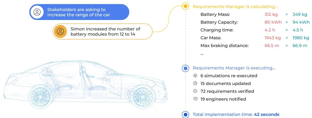
An essential aspect of requirements management is its ability to de-risk projects from unexpected and late-stage requirement changes. For instance, consider the complex process of car design. If a stakeholder requests an increase in the vehicle’s range, it would necessitate various adjustments, such as increasing the number of battery modules. A tool for managing compliance statuses, like the Altium 365 Requirements Manager, automatically recalculates all relevant properties, like battery mass and capacity, and adjacent properties, such as charging mass, car mass, and braking distance, ensuring full traceability of the change and its system-wide impact.
In a traditional setting, accommodating a new requirement would involve a tedious chain of meetings, emails, and manual updates, often extending over weeks. With a proficient requirements management tool, you can drastically reduce this time because every team member is aligned, informed, and working on the latest, most accurate information within seconds. All aspects of the design are consistently synchronized, and no detail is overlooked or forgotten in the fast-paced development lifecycle. You can finish your car design updates within a minute instead of weeks of disjointed, back-and-forth communication.
While the concept of requirements is easy to grasp, the speed and complexity of modern design development complicate the overall picture. We’re witnessing an unprecedented pace of technological advancement and a surge in the intricacy of electronic designs. This evolution, while exciting, brings forth a multitude of challenges that necessitate a structured approach to requirements management.
#1 Complexity of Electronic DesignsThe proliferation of smart devices has exponentially increased the complexity of electronic designs. For instance, chip usage in products has skyrocketed, with modern vehicles incorporating over 2,000 chips, a staggering increase compared to a few decades ago. Such complexity necessitates precise and well-organized requirements to navigate the intricate web of design elements, ensuring that each component integrates smoothly to function as a cohesive whole.
The more complex the product, the more critical becomes the significance of requirements management. This is because more time and budget are invested in its development. The cost of getting it wrong—be it money, time, or reputation—is too great to risk.
#2 Growing Software InterconnectionSoftware has become an integral part of products, with the lines of code embedded in them soaring fifteenfold over the last decade. Software acts as the communication bridge, enabling various hardware systems to exchange critical information. This intricate web of interconnectivity demands well-established communication protocols to secure the uninterrupted flow of essential data. An unexpected alteration in the requirements of one system can disrupt this harmonious interaction, leading to unforeseen complications and extensive rework. Thus, the role of requirements management becomes crucial in safeguarding the stability and reliability of these interconnected systems to maintain the integrity of the overall communication network.
#3 Reduced Production TimelinesThe urgency to expedite product delivery has led to a significant reduction in production timelines. Traditional five-year cycles have been compressed to two, calling for agile methodologies that emphasize swift iterations and continuous improvement. In such a fast-paced environment, having clear and well-defined requirements is crucial to guide the design process efficiently and facilitate quick decision-making.
#4 Communication Gaps and Siloed ProcessesDesign processes have been plagued by communication gaps, with electronic data often existing in isolated silos. The exchange of information between these silos is a manual and inefficient process, leading to the unnecessary expenditure of valuable time and resources and compromising the overall quality of the product. A robust requirements management system acts as a unifying thread, enhancing communication and ensuring all design aspects are aligned and integrated.
#5 Lack of TraceabilityIt’s quite common for as many as 80% of designs to experience last-minute changes in components due to constraints related to cost or availability. The absence of traceability in such modifications can lead to confusion and errors, often derailing the entire design process. Requirements management fosters traceability and ensures that each modification is documented and aligned with the overall design objectives, thus minimizing mistakes and enhancing the design’s integrity.
7 Reasons Requirements Management Is EssentialAs you see from the above analysis, requirements management is not optional. It’s essential to secure the project’s success, especially in light of the fact that poor requirements trigger 70% of project failures. Inaccurately defined requirements can lead to expanding project scopes, delayed timelines, escalated costs, and a final product that falls short of meeting customer expectations and safety standards. Adopting a structured attitude toward their management can prevent your project from becoming another failure in the quoted statistics.

Requirement management clarifies the project’s objectives, aligning stakeholders like product managers, designers, developers, and clients towards a unified goal. It provides a clear roadmap, outlining the project’s scope, budget, and schedule, ensuring that every step is well-planned and executed according to the established objectives and expectations.
#2 Faster DeliveryManaging compliance status promotes timeliness, helping projects stay on schedule for quicker delivery while upholding quality standards.
#3 ReusabilityRequirements management allows for the reuse of specific project components in subsequent projects, enhancing sustainability and efficiency throughout development.
#4 Improving Quality and Reducing ErrorsA clear set of requirements minimizes errors, misunderstandings, and omissions in the design process, ensuring that the final product meets expected quality standards and fulfills its intended purpose. Requirements management enhances the alignment of the end product with customer needs and expectations, thereby improving its overall quality.
#5 Lower Cost of Development Across the LifecycleLifecycle Insights reports that companies, on average, encounter 2.8 board respins, each costing approximately $46,000. Errors in requirements often necessitate extensive rework by the development team. The cost of correcting a software error escalates if the mistake is detected later in the process. The necessity to reduce these costs is beyond question, and strategies that minimize requirement discrepancies are most welcome.
Effective requirements management enhances project efficiency and accuracy. It minimizes unnecessary expenses throughout the project, leading to a more economical development process. It also aids in reducing the frequency of costly and time-consuming modifications, saving both money and months of extra work.
#6 Risk ManagementRequirements management helps identify potential risks early in the project, allowing for implementing strategies to mitigate them.
#7 Facilitating Communication and CollaborationWorking with a transparent and well-managed set of requirements fosters effective communication and collaboration among team members and stakeholders. It acts as a common language, improving understanding and cooperation across various domains of expertise.
Design Faster with Fewer ErrorsThe complexities and rapid advancements in modern design call for a strong foundation in requirements management. A well-organized set of specifications supports the process by providing clarity, enhancing communication, and ensuring that the design evolves cohesively in the desired direction. Check it on your own using Requirements Manager. Design faster with fewer errors!
The post The Challenges of Modern Design: Why Requirements Management Is Essential appeared first on ELE Times.
Zypp Electric registers 3X revenue growth in FY24; deploys 20,000 e-scooters across India in 2023, goes operationally profitable
Zypp Electric, India’s leading tech-enabled EV-as-a-service platform, has marked a remarkable milestone with a staggering ~3X surge in revenue in FY24. This exponential growth underscores Zypp Electric’s unwavering commitment to transforming last-mile deliveries through sustainable mobility solutions. Having emerged as the number one ranked company in the entire list of Asia-Pacific 2024’s fastest-growing businesses, Zypp Electric has achieved a remarkable 396% compound annual growth rate (CAGR) from 2019 to 2022.
By successfully deploying an additional fleet of electric scooters across India, Zypp Electric has expanded its presence in six major metropolitan cities of Delhi NCR, Bangalore and Mumbai. The increase from 11,000 to more than 20,000 electric vehicles showcases the company’s dedication to sustainable logistics & mobility platform.
By collaborating with quick-commerce, food delivery, bike taxi, e-commerce and other online businesses, the company has been progressively working to ensure 100% electric last-mile deliveries in India, Zypp Electric has done 45 million+ shipment deliveries via electric vehicles from Jan’23 to Feb’24 period which equates to growing 76 Lakh trees on the planet earth. Over the past year, we have empowered more than 53,000 delivery executives to adopt an electric vehicle, with an opportunity to earn more on our platform. There has also been a notable rise in their monthly average earnings per rider, amounting to more than INR 24,000/month and allows them to save 50% more than petrol bike riders. Their environmentally friendly initiatives have led to a significant reduction of 29 million kilograms of carbon emissions since the start of its operations
A few of the key drivers of Zypp Electric’s unprecedented growth have been its core focus on a technology platform encompassing the entire EV ecosystem and its strategic expansion into new markets. From being the leader in the National Capital Region (NCR), Zypp Electric has successfully penetrated additional markets, including Bangalore, Mumbai, and now in Hyderabad too. This expansion not only signifies the company’s agility and adaptability but also its ambitious vision to revolutionise electric last-mile logistics across multiple urban landscapes.
Moreover, Zypp Electric’s foray into the three-wheeler cargo business further solidifies its position as a frontrunner in the EV sector. E3W fleet has grown 6X from Feb’23 to 750+ in Feb’24 and deliveries have increased from 4,320 to 92,000+ in the same period clocking 21X growth. By diversifying its portfolio, with a fleet of soon-to-reach 1000 electric L5 loaders & expanding, Zypp Electric is poised to cater to a wider range of business needs while maximising revenue streams along with branding options on the E3W open for advertising option.
In addition to its expansion endeavours, Zypp Electric has achieved operational profitability, a testament to its robust business model and strategic foresight. With a keen focus on sustainable growth, the company is now on the verge of reaching breakeven over the next 12 to 18 months, setting a solid foundation for long-term success.
Commenting on the company’s stellar performance, Akash Gupta, Co-Founder & CEO, of Zypp Electric, remarked, “The last fiscal year has been momentous for us. We grew our revenues almost 3X vs. the last fiscal year which I am super proud of for our team to achieve this milestone amid the changing EV landscape. While ramping things up in NCR & Bengaluru by adding more hubs, we initiated our operations in Mumbai this year. Looking ahead, we’re excited to commence our services in Hyderabad & target to launch in a new city every quarter. On the fleet front, we intend to grow our current strength of 20,000 to around 100,000 vehicles in the next 12 to 18 months and then grow that to 500,000 over the following 36 to 48 months. Profitability is the next major milestone which we’re eyeing closely at Zypp along with growth.”
Recently, Zypp Electric has also entered into a partnership with Porter Enterprises to provide reliable logistics solutions. With a robust foundation, strategic expansions, a superlative EV Fleet Management technology platform and a relentless pursuit of innovation, Zypp Electric is poised to reshape the landscape of last-mile deliveries and accelerate the transition towards a sustainable future.
The post Zypp Electric registers 3X revenue growth in FY24; deploys 20,000 e-scooters across India in 2023, goes operationally profitable appeared first on ELE Times.
Microchip Technology Introduces ECC608 TrustMANAGER with Kudelski IoT keySTREAM
Cloud-based software as a service leverages secure authentication ICs to enable self-service custom PKI, streamlined in-field provisioning and lifecycle management for IoT devices
As the world comes to rely on interconnected IoT systems—for everything from household items like smart thermostats, virtual assistant technology and digital door locks to medical and industrial applications—the need for reliable cybersecurity on embedded systems has never been greater. To increase security on IoT products and facilitate easier setup and management, Microchip Technology has added the ECC608 TrustMANAGER with Kudelski IoT keySTREAM, Software as a Service (SaaS) to its Trust Platform portfolio of devices, services and tools.
With security credentials managed and updated in the field via keySTREAM—instead of being limited to a static certificate chain implemented during manufacturing—the ECC608 TrustMANAGER allows custom cryptographic credentials to be accurately provisioned at the end point without requiring supply chain customization and can be managed by the end user. keySTREAM offers a device-to-cloud solution for securing key assets end-to-end in an IoT ecosystem throughout a product’s lifecycle.
The ECC608 TrustMANAGER relies on a secure authentication IC that is designed to store and protect cryptographic keys and certificates, which are then managed by the keySTREAM SaaS. The combined silicon component and key management SaaS allow the user to set up a self-serve root Certificate Authority (root CA), and the associated public key infrastructure (PKI) secured by Kudelski IoT, to create and manage a dynamic certificate chain and provision devices in the field the first time they are connected. Once claimed in the SaaS account, the devices are automatically activated in the user’s keySTREAM service via in-field provisioning.
“As the volume of connected devices rapidly increases and security standards and regulations tighten, IoT designers are seeking more efficient ways of managing their devices once products are in their customers’ hands,” said Nuri Dagdeviren, corporate vice president of Microchip’s security computing group. “Our partnership with Kudelski and adding keySTREAM to our ECC608 TrustMANAGER enables customers to manage, scale and update IoT ecosystems efficiently via a cloud-based security SaaS for in-field provisioning and certificate management.”
Security standards and upcoming regulations are increasingly requiring upgradability of security infrastructure for IoT devices. This is a difficult task with traditionally static IoT security implementations, which require physical upgrades like changing out the security ICs in each device to stay in compliance. With the ECC608 TrustMANAGER, the process is automated and highly scalable, allowing devices to be managed securely and efficiently throughout their lifecycle. It also enables easy device ownership management without needing to change hardware, as security keys are updated digitally from the cloud into the device. This approach streamlines the supply chain processes for distribution partners as well.
“The ECC608 TrustMANAGER with keySTREAM marks a pivotal moment in our quest to secure the IoT landscape and make provisioning easier. Our collaboration with Microchip is not just about bringing advanced security solutions to the market, it’s about setting a new standard for smart device security across the board,” said Hardy Schmidbauer, senior vice president of Kudelski IoT. “By leveraging Microchip’s renowned semiconductor technologies alongside Kudelski IoT’s security services, we are poised to deliver protection and a new ease of provisioning for IoT device manufacturers.”
This type of dynamic in-field provisioning and device management meets IoT security standards and will be useful in device certificate updates needed to stay in compliance with evolving security requirements. The keySTREAM SaaS allows for ongoing updates of keys designed to prevent and protect against evolving threats and security requirements. In-field provisioning also removes the need for customization for more efficient manufacturing.
The ECC608 is the first security IC in Microchip’s TrustMANAGER series. To get started, download the Trust Platform Design Suite and test the keySTREAM use case under the ECC608 TrustMANAGER.
The post Microchip Technology Introduces ECC608 TrustMANAGER with Kudelski IoT keySTREAM appeared first on ELE Times.
Infineon and Green Hills Software present integrated platform for real-time applications for software-defined vehicles
Infineon Technologies and Green Hills Software LLC, the global leader in embedded safety and security, have launched an integrated microcontroller-based processing platform for safety-critical real-time automotive systems. The platform combines the safety-certified real-time operating system (RTOS) µ-velOSity from Green Hills with Infineon’s new generation of safety controllers AURIX TC4x. This provides OEMs and Tier 1 suppliers with a reliable, safe, and secure processing platform to develop domain and zonal controllers as well as drivetrains for electric vehicles for their next-generation software-defined vehicle (SDV) architectures.
“Green Hills’ product philosophy for tools and the matching software environment support our requirements for reliable products and solutions very well,” said Thomas Schneid, Senior Director for Software, Partnership and Ecosystem Management at Infineon. “Combined with advanced microcontroller products such as the AURIX TC4x family, our customers gain a significant advantage in meeting their critical requirements.”
“We are excited to extend our long-standing collaboration with Infineon and showcase our joint solution at embedded world 2024,” said Dan Mender, Vice President of Business Development at Green Hills Software. “The combination of Infineon’s new scalable microcontroller family AURIX TC4x and Green Hills’ µ-velOSity RTOS will enable our joint customers to develop safe and secure systems for the next generation of SDV E/E architectures.”
Enabling the development of advanced ECUs
New automotive electronic control units (ECU) are essential for the adapted vehicle E/E architecture of SDVs. To develop these ECUs, new microcontrollers are needed that also meet the requirements of safety-critical systems such as zone control, chassis, radar, electric drives, and affordable AI systems, by offering higher performance and advanced features. Infineon addresses this demand with its new family of AURIX TC4x devices that complement its TriCore multicore architecture with a safety and security accelerator suite. Moreover, to meet the stringent safety requirements, Green Hills has ported its safety-certified µ-velOSity RTOS to the AURIX TC4x family. The advanced MULTI integrated development environment is also supporting this processor family, enabling developers to shorten development times by increasing developer productivity while generating the fastest and smallest code for the AURIX TC4x.
Infineon’s AURIX TC4x family provides an upward migration path from the previous AURIX TC3x family of ASIL-compliant automotive MCUs. AURIX TC4x uses the next-generation TriCore 1.8 and a scalable accelerator suite, including the new Parallel Processing Unit (PPU) as well as several intelligent accelerators, in areas such as data routing, digital signal processing, radar processing and cryptographic computing. The AURIX TC4x family supports high-speed interfaces, including Gigabit Ethernet, PCIe, CAN-XL or 10BASE T1S Ethernet, to provide sufficient communication bandwidth for the next generation of automotive systems.
The Green Hills µ-velOSity RTOS targets the highest functional safety levels (ISO 26262 ASIL D). Based on an efficient and reliable kernel with a minimal footprint and a simple API, it also offers fast boot and streamlined execution. In addition, µ-velOSity is tightly integrated with the MULTI safety-certified tools and compilers.
Demonstration at the embedded world 2024
Green Hills and Infineon will showcase their solution at embedded world 2024, April 9-11, at the Green Hills booth 4-325.
Infineon at Embedded World
embedded world will take place in Nuremberg, Germany, from 9 to 11 April 2024. Infineon will present its products and solutions for decarbonization and digitalization in hall 4A, booth #138 and virtually.
The post Infineon and Green Hills Software present integrated platform for real-time applications for software-defined vehicles appeared first on ELE Times.
MIKROE Partners With Allegro MicroSystems To Introduce New Click Boards Targeting Industrial Applications
MikroElektronika (MIKROE), the embedded solutions company that dramatically cuts development time by providing innovative hardware and software products based on proven standards, has announced that the company is closely collaborating with Allegro MicroSystems, Inc. (“Allegro”), a global leader in power and sensing solutions for motion control and energy-efficient systems, to offer a broad portfolio of products that reduce development effort and accelerate time to market. Over the last quarter, MIKROE has introduced three new, compact, Click add-on boards incorporating Allegro’s technology.
“As a third-party tool provider we strive to promote our partners’ newest technologies and products, by making them simple to use in the broad market,” said Nebojsa Matic, CEO of MIKROE. “We are delighted to collaborate with Allegro and look forward to introducing many more Click boards utilizing their sensor technology in the near future.”
Hall Current 17 Click:
A compact add-on board that contains a precise solution for AC/DC current sensing, the Hall Current 17 Click board features the ACS37010, a high-accuracy current sensor from Allegro. This Click makes the perfect solution for the development of applications requiring a combination of high-current monitoring and high isolation voltage between the primary high-current and low-voltage sides.
Angle 9 Click:
Designed to detect the absolute position of a permanent magnet, this board features the AAS33001, Allegro’s precision, contactless angle sensor with incremental and motor commutation outputs and on-chip linearization for 0° to 360° angular position, rotation speed, and directional measurement. Support for incremental output interface (ABI) and motor commutation (UVW) is also available. On-chip EEPROM enables factory and customer calibration parameters to be stored. This Click board is the perfect solution for the development of contactless potentiometers, contactless knobs, RC servos, and other angular position measurement solutions.
Hall Current 16 Click:
A precise solution for AC/DC current sensing, this board is based on the ACS37002, a 400kHz high-accuracy current sensor from Allegro that features pin-selectable gains that can be used to configure the device to one of the four defined sensitivities and
corresponding current ranges, increasing design flexibility. In addition, an adjustable overcurrent fast fault provides short-circuit detection. This Click board facilitates the development of applications requiring a combination of high-current monitoring and high isolation voltage between the primary high-current and low-voltage sides.
“We are thrilled to partner with MIKROE as they release three new easy to use development tools that incorporate our industry-leading magnetic current and angle sensors,” said Ram Sathappan, Senior Director, Applications Marketing at Allegro. “We anticipate a very strong interest, as these sensor Click boards enable our customers to quickly develop innovative end products requiring high accuracy and reliability, without having to develop their own hardware.”
Like all Click boards from MIKROE, the solutions featuring Allegro’s sensor technology are packaged with mikroSDK software and a library with all the functions. The Clicks come fully tested and approved prototype, making them reliable devices ready to use on the development board. This can cut months from the development cycle and save considerable expense.
The post MIKROE Partners With Allegro MicroSystems To Introduce New Click Boards Targeting Industrial Applications appeared first on ELE Times.
Anritsu Enhances Protocol Test Solution Supporting NTN NB-IoT Devices for GEO Satellites
Anritsu Corporation introduces the protocol test[*1] solution for Non-Terrestrial Network (NTN)[*2] devices for GEO[*3] satellites, which extends the functionality of the Signalling Tester MD8430A to support the NTN NB-IoT[*4] defined in 3GPP Release 17.
Anritsu has been providing solutions for protocol tests, RF tests, protocol conformance tests, and RF conformance tests over the years for 3G/LTE/5G. With this functionality enhancement, Anritsu will help to improve the quality of NTN devices and contribute to the realization of a prosperous network society.
Development BackgroundPreviously, individual satellite operators have offered their proprietary unique satellite communication services. Since the standardization of NTN communications in 3GPP Release 17, however, the satellite communication service market has rapidly grown, and various verifications based on the standard specifications have become necessary. For GEO satellites, NTN device vendors need test environments that can simulate the communication delay and transmit information to the device for delay compensation, because the distance between the satellite and the device is approximately 36,000 km. To support these test requirements, Anritsu has developed a protocol test solution that boasts high reliability built on test experiences with market-leading customers and high flexibility in condition settings.
Product OutlineThe MD8430A is a base station simulator that can build a simulated network necessary for the development of chipsets and devices. With its software option NTN NB-IoT (GEO) MD8430A-043 and its control software option NTN over IoT Framework for RTD MX800050A-070, the MD8430A can be connected to an NTN device for GEO satellites, which makes it possible to test the connection with the NTN network and roaming between the terrestrial network and NTN network, among others.
Technical Terms[*1]: Protocol test
Protocol sequence test (location registration, call placement, incoming call reception, mobile device/network disconnection, handover, etc.)
[*2]: NTN
Abbreviation for Non-Terrestrial Network. It refers to a communication network system that provides multi-layered connections among mobile devices on the ground as well as in the sea, skies, and outer space. The NTN can efficiently cover locations that are difficult for radio signals from terrestrial base stations to reach, such as remote islands, oceans, and mountains, thus delivering Internet access to underserved areas.
[*3]: GEO
Abbreviation for Geostationary Earth Orbit
[*4]: NB-IoT
Abbreviation for NarrowBand Internet of Things. It refers to a technology that enables a host of IoT devices to connect to the network with low power consumption. NTN NB-IoT is an IoT communication service for areas that terrestrial base stations cannot cover and is used in such fields as maritime shipping, logistics, mining, and automobiles.
The post Anritsu Enhances Protocol Test Solution Supporting NTN NB-IoT Devices for GEO Satellites appeared first on ELE Times.
Microchip Technology Expands Its Serial SRAM Portfolio to Larger Densities and Increased Speeds
Product line offers a lower-cost alternative to parallel SRAM with up to 4 Mb density and 143 MHz SPI/SQI communications
To address a common customer need for bigger and faster SRAM, Microchip Technology has expanded its Serial SRAM product line to include larger densities of up to 4 Mb and increased Serial Peripheral Interface/Serial Quad I/O Interface (SPI/SQI) speed to 143 MHz. The 2 Mb and 4 Mb devices are designed to provide a lower-cost alternative to traditional parallel SRAM products and include optional battery backup switchover circuitry in the SRAM memory to retain data on power loss.
Unlike parallel RAM, which requires large packages and at least 26–35 microcontroller (MCU) I/Os to interface, the Microchip serial SRAM devices come in a lower-cost, 8-pin package and utilize a high-speed SPI/SQI communication bus that only requires 4−6 MCU I/O pins for easy integration. This reduces the need for a more expensive, high-pin-count MCU and can help minimize the overall board footprint.
Addressing the most common drawback to serial SRAM—that parallel is faster than serial memory—the 2 Mb and 4 Mb serial SRAM devices have increased the bus speed capability to 143 MHz with optional quad SPI (4 bits per clock cycle), which greatly minimizes the speed gap between solutions.
“Serial SRAM is a popular solution for engineers who need more RAM than what is available on board their MCU but are looking to reduce cost and overall board size,” said Jeff Leasure, director of Microchip’s memory products business unit. “Microchip’s 2 Mb and 4 Mb serial SRAM devices are intended to replace expensive parallel SRAM with an easy and cost-effective alternative.”
The small-form-factor, low-power, high-performance serial SRAM devices have unlimited endurance and zero write times, making them excellent options for applications involving continuous data transfer, buffering, data logging, metering and other math- and data-intensive functions. These devices are available from 64 Kbit up to 4 Mb in density and support SPI, SDI and SQI bus modes. Visit Microchip’s Memory Products page to learn about the company’s full portfolio of memory devices.
The post Microchip Technology Expands Its Serial SRAM Portfolio to Larger Densities and Increased Speeds appeared first on ELE Times.
Vicor to present modular power conversion solutions for 48V Zonal Architectures at WCX 2024
High-density, 800V and 48V scalable power modules solve electrification power conversion challenges
As the automotive industry moves toward 48V zonal architectures, power system design engineers are looking for new high-voltage power conversion solutions that have leading power density, weight and scalability attributes.
Vicor will be presenting five papers at World Congress Experience 2024 (WCX) in Detroit on April 16 – 18, detailing its innovative approach to 800V and 48V power conversion using new high-density, scalable power modules with proprietary topologies and innovative packaging.
The Vicor papers are:
- Achieving EM conducted emission compliance for high-voltage conversion with switching frequency above 1.3MHz
Presented by: Nicola Rosano, Sr. Strategic System Engineer, EMEA - Designing 48V zonal architecture that keeps the high voltage inside the BEV battery pack
Presented by: YK Choi, Sr. Field Application Engineer, Vicor, APAC
Kang YoungJae, Chief Engineer, INFAC
- Eliminating the high-voltage precharge with existing hardware in BEV
Presented by: Patrick Kowalyk Automotive, Principal Field Application Engineer, North America
- Migrating to 48V with high efficiency, power density and efficient system cost
Presented by: Patrick Wadden, Global VP, Automotive Business Unit
- The uncertain future of aftermarket loads in a 48V world
Presented by: David McChesney, Strategic Account Manager, North America
The post Vicor to present modular power conversion solutions for 48V Zonal Architectures at WCX 2024 appeared first on ELE Times.
Delta India Partners with BMRCL for the Development and Naming Rights and of the Bommasandra Metro Station in Bangalore, Pioneering Sustainable Urban Mobility
Over two decades deploying Delta’s smart energy-saving solutions to support the rapid transformation of India’s e-mobility, renewable energy, and manufacturing sectors
In a momentous occasion commemorating its 20th anniversary in India, Delta Electronics India Pvt Ltd (Delta India) announced a transformative partnership with Bangalore Metro Rail Corporation Limited (BMRCL). The two entities have signed a Memorandum of Understanding (MoU) for the naming rights of the Bommasandra Metro Station on the yellow line of RV Road to Bommasandra Line (Reach-5) as part of Phase-II of the Bangalore Metro Rail Project.
Under this agreement, Delta India will contribute Rs. 65 Crores towards the construction of the Bommasandra Metro Station, with an initial payment of Rs. 10 Crores already made. As per the agreement, BMRCL will be offering the naming rights of Bommasandra Metro Station as ‘Delta Electronics- Bommasandra Metro Station’ for a period of 30 years
Mr. Benjamin Lin, President of Delta Electronics India, remarked, “We are incredibly proud to have the opportunity to contribute to the sustainable development of Bengaluru. Partnering with BMRCL on the Bommasandra Metro Station aligns perfectly with our global commitment to fostering sustainable cities. This new station will provide much-needed connectivity for residents and commuters, while also promoting a cleaner and more efficient transportation system for the city.”
Delta Electronics Inc. is a global leader in power management and a provider of IoT-based smart green solutions. Mirroring this commitment to environmental protection, Delta India has actively promoted energy-efficient products and services nationwide for the past two decades. This investment in the Bommasandra Metro Station further exemplifies Delta India’s dedication to supporting sustainable urban development in Bangalore.
Mr. M. Maheshwar Rao, Managing Director, BMRCL, expressed his delight about the partnership, stating, “We are delighted to partner with Delta Electronics India on this crucial infrastructure project. Their contribution of Rs. 65 Crores for the Bommasandra Metro Station signifies remarkable support for sustainable urban development. This innovative financing mechanism sets a valuable precedent for future collaborations. We commend Delta India for their dedication to sustainability and look forward to working together to create a more connected and environmentally conscious city.”
The development of the Bommasandra Metro Station through Delta India’s contribution showcases a ground-breaking approach to infrastructure projects. This collaboration demonstrates the immense potential for private sector participation in accelerating the expansion to infrastructure projects.
Mr. Niranjan Nayak, MD, Delta Electronics India Said, ” We are thrilled to collaborate with BMRCL on this innovative project that aims to revolutionize sustainable urban mobility in Bangalore. Through this partnership, Delta India is committed to enhancing the commuting experience for residents while promoting eco-friendly transportation solutions. We look forward to contributing to the growth and development of the city through this exciting initiative.”
The Bommasandra Metro Station is part of the 19.15 km yellow line under Phase II of the Bangalore Metro Rail Project. This line, connecting RV Road to Bommasandra with 16 stations, is being constructed at a cost of INR 5744 Crores. Upon completion, the Yellow Line will provide a sustainable and efficient transportation alternative for residents and commuters across Bangalore. This will significantly reduce traffic congestion on Hosur Road, leading to a substantial decrease in vehicular pollution and a cleaner, greener city.
The collaboration between BMRCL and Delta Electronics India for the construction of Bommasandra Metro Station marks a significant step forward in expanding Bangalore’s metro network and promoting sustainable urban development. This project serves as a shining example of the positive impact that can be achieved through public-private partnerships focused on innovation and environmental responsibility. As Delta India celebrates 20 years of success in India, this initiative underscores their unwavering commitment to building a sustainable future for the city and its residents.
The post Delta India Partners with BMRCL for the Development and Naming Rights and of the Bommasandra Metro Station in Bangalore, Pioneering Sustainable Urban Mobility appeared first on ELE Times.
Industry 4.0: Integrative use of data for maximized ROI
Courtesy: ASMPT
Information is increasingly becoming critical for success in modern SMT production. To get the most out of your manufacturing equipment, you must collect data across the board, process it in a user-oriented manner, and make it available in the right place. Advances in SMT production are characterized by increases in automation, standardization, and integration. While the early days of electronics manufacturing were marked by an approach that featured lots of manual support and was insular and closed-off in terms of information technology, a strong trend towards automation has developed in recent years that is driven by high personnel costs and a shortage of skilled workers due to demographic factors.
The people-free “lights out” factory, however, turned out to not be a sensible optimization goal for economic reasons alone because automation lowers unit costs only to a certain degree. Over-automation, on the other hand, drives up costs. In practice, the Pareto principle, which states that 80 percent of the results are achieved with 20 percent of the resources employed, applies here as well. Each additional percentage point of improvement requires a disproportionate increase in resources. ASMPT recognized this early on and reached the first stage with the Integrated Smart Factory, which focused on maximizing the return on investment instead of automation.
Interfaces as development driversThe introduction of standardized interfaces to improve the manufacturing processes in the Integrated Smart Factory was an essential factor for the increasing integration of existing hardware and software solutions. Of particular importance are:
• IPC-HERMES-9852 for the seamless machine-to-machine (M2M) communication
• IPC-2591 CFX for linking machines and autonomous storage and transport systems to higher-level systems such as MES and ERP
The global innovation and market leader uses these standard industrial interfaces for its open and flexible automation concept which easily integrates third-party systems, enables retrofits, and gives electronics manufacturers the freedom to choose how, when and to what extent they want to automate their production. With this strategy, electronics manufacturers are precisely geared to the needs of users and the market in terms of their degree of digitalization and automation. The approach was subsequently complemented with software solutions for personnel deployment, quality assurance and material logistics.
The Integrated Smart Factory already features direct machine-to-machine communication – for example, the SPI system can trigger offset corrections or cleaning cycles in the solder paste printer without user intervention. The individual production and quality assurance stages, however, are still largely isolated from each other. In addition, an important resource is hardly used in an integrative way: the data that the numerous cameras, sensors and readers on the individual machines continuously produce.
In contrast to pure machine manufacturers or pure software developers, ASMPT as a system supplier covers almost the entire SMT production with its products, has unique process know-how, and knows from many years of experience which data from the production ‘data lake’ is truly relevant.
By advancing the Integrated Smart Factory into the intelligent factory, ASMPT is now leveraging this treasure trove of data and consistently using big data to optimize the return on investment both in depth, i.e., in the form of more detailed production process analysis and optimization, and across the board through the data-based integration of production areas such as the company’s intralogistics.
It is no longer just the individual process step, the individual machine, the individual setup, the individual product or the individual material requirement that is being considered, but the SMT production in its totality. This new concept of integrative data use in the intelligent factory brings benefits on several levels.
The basis of any improvement in SMT production is the continuous collection and presentation of key performance indicators (KPIs). These include, for example, the line’s throughput rate, overall equipment efficiency (OEE), utilization, and balance. To make this possible, the intelligent factory accumulates machine data in a monitoring application that is part of ASMPT’s Works software suite and makes it available in a way that is role-specific and device-independent.
With their SPI and AOI systems, modern production lines already have highly powerful quality assurance systems. Unfortunately, many of the faults they detect do not originate where they are first discovered. While these systems were able to reject faulty products, they often did not help in eliminating the underlying problems. In the intelligent factory, on the other hand, easy-to-use overarching dashboards quickly reveal what led to these errors. The data integration extends beyond the line. By comparing planning, reference and real-time production data, production obstacles are identified and can be eliminated – again through comprehensive analyses.
The M2M data flow delivers another plus in user-friendliness: Since faults that have been detected by WORKS’ multi-line analysis functions appear on the display of the affected machine, the maintenance staff knows right away where they need to take action.
Since providing the right material in the right quantity at the right time in the right place has always been the goal of intralogistics, the integrative use of data in the intelligent factory has also revolutionized the flow of materials. For example, it is now possible to continuously compute the material consumption on the line in real time in freely definable time slices. The system combines and correlates data on planned and actual material consumption along with data on material currently along the line. Based on this information, WORKS generates material requests to the central and local storage sites along with time-controlled transportation orders. In this way, space-consuming “emergency stock” on the line can be avoided, and the material is available on time and exactly where it is actually needed.
Material buffering in the setup preparation area can also be optimized easily and efficiently with WORKS. Once a production order has been completed, the software provides the employees on the line with detailed instructions as to which component reels need to be returned to the warehouse and which should remain in the setup preparation area because they will be needed again for one or more subsequent orders. This saves time and unnecessary material travel between the shop floor and the central warehouse.
The factory-encompassing management and coordination of autonomous storage and transport systems for all production-relevant materials and tools – from the receiving of materials to the shipping of finished products – is now data-based as well.
A good practical example of the benefits of the integrative use of data is the setup changeover for a new product. In the intelligent factory, the line no longer needs to be emptied – the program changeover can be executed automatically by passing the data of the circuit board being processed from machine to machine via the standardized IPC-HERMES-9852 interface.
As soon as the PCBs are unloaded from the magazine at the start of the line, all relevant data is sent to the DEK TQ solder paste printer from ASMPT. This can be done via labels and a barcode reader or directly from the production planning system. The machine then compares the data with the information stored in the planning system. If necessary, it triggers an automatic program download and any setup changes that may be required. Once printed, the circuit board is passed along to the Process Lens SPI system along with its IPC-HERMES-9852 data and subsequently to the SIPLACE placement machines. Each manufacturing station executes a new comparison between the loaded and the required program and makes any necessary updates. Thanks to these PCB-induced program changeovers, multiple products can be manufactured simultaneously on a single line. Even the conveyors adapt automatically to the width of the circuit boards being transported. And in case of a family setup, these product changeovers can be executed with no operator assist whatsoever.
The intelligent factory does more than control the machines based on data – it also supports the most important production resource of all: people. Scarce specialists are no longer tied to a specific line but can be deployed across the entire shop floor based on their soles and qualifications. To do this, the state-of-the-art staff management application in WORKS interfaces with the material flow planning system. If, for example, manual support is required for a setup change, a corresponding request appears on an operator’s device automatically and with sufficient lead time. And if the task can be carried out remotely, this is done conveniently via a remote cockpit. In this way, SMT lines can be kept running continuously, making the whole factory more productive. With software for all of the factory’s maintenance and repair tasks, teams of technicians can easily balance on-demand maintenance and ongoing production tasks, effectively managing all assets from whole machines to individual nozzles. When unforeseen problems arise, an AI- and NLP-based virtual assistant with an extensive knowledge base supports root cause research and troubleshooting – and best of all, you can simply ask it questions using your voice, just like talking with an experienced colleague.
“Thanks to standardized interfaces, what belongs together is now growing together in the intelligent factory,” says Bernhard Fritz, Head of Global Marketing at ASMPT SMT Solutions. “Material flow and quality management, planning and the factory floor, man and machine – all production factors are merging into an integrative whole. And the overarching improvement goal is always the best possible utilization of existing capacities – and above all, the maximum return on investment.”
The post Industry 4.0: Integrative use of data for maximized ROI appeared first on ELE Times.
New Tech Tuesdays: Transitioning Renewable Energy to 1500V with DC/DC Converters
The global renewable energy market has been experiencing substantial growth, driven by the increasing demand for clean and sustainable energy sources. Solar energy, in particular, has gained prominence as a key player in the renewable energy landscape. According to a report by Mordor Intelligence, the renewable energy market has now reached pre-pandemic levels, signifying its resilience and continued growth. This growth is attributed to various factors, including government incentives, technological advancements, and an increased awareness of environmental concerns.
The industry is constantly evolving to further enhance the efficiency and financial viability of photovoltaic (PV) systems. One critical aspect of this evolution is the need for 1500VDC PV systems. However, this transition presents challenges for DC-DC converters in supporting higher voltages. This week, we explore the progression and recent challenges of PV systems and consider how the solar market stands to benefit significantly from the AE15B-EW and AE15B-UW DC-DC converters from CUI Inc.
The Evolution of Photovoltaic SystemsTo remain competitive and sustainable, photovoltaic systems must continuously improve their efficiency and financial viability. This drive for improvement stems from several considerations.
First, maximizing energy output. Efficiency is fundamental in solar energy generation. By increasing the efficiency of PV systems, more energy can be harnessed from the same amount of sunlight. This leads to higher energy production and better returns on investment. Facilities like the National Renewable Energy Laboratory (NREL), part of the US Department of Energy, regularly conduct testing of PV cells (Figure 1) and modules to ensure consistency and accuracy of PV performance metrics.
 Figure 1: Graph showing the highest confirmed conversion efficiencies across a range of photovoltaic technologies, spanning 1976 to the present. (Source: National Renewable Energy Laboratory).
Second, reducing the installation costs. Financial viability is a crucial aspect of any solar project. Lowering installation costs, such as hardware and labor, can make solar energy more affordable for consumers and businesses alike. This is essential for the widespread adoption of solar technology.
Lastly, adapting to new technologies. The solar industry must continually adapt to emerging technologies, such as advanced materials and improved manufacturing processes. These innovations contribute to both increased efficiency and reduced costs.
The Need for 1500VDC Photovoltaic SystemsOne significant development in the solar industry is the transition from traditional 1000VDC PV systems to 1500VDC PV systems. This increase in voltage has several advantages. Primarily, it improves the overall energy transmission. Stepping up to higher voltage systems allows for efficient electricity transmission over longer distances. This is particularly beneficial for large-scale solar installations and solar farms. Increasing the voltage also helps to mitigate electrical losses during energy transmission, resulting in less energy waste, thereby contributing to higher overall system efficiency. Also, 1500VDC systems require fewer electrical components, such as cables and connectors, leading to cost savings during installation and maintenance.
Challenges for DC-DC Converters in 1500VDC SystemsWhile the transition to 1500VDC PV systems offers numerous benefits, it also presents challenges for DC-DC converters, which play a critical role in these systems. For instance, DC-DC converters must be capable of handling the increased voltage levels in 1500VDC systems. This requires robust and reliable components to ensure safety and system stability.
Also, system efficiency is critical. Maintaining high efficiency levels in DC-DC converters is essential to maximize the energy harvested from solar panels. Any loss in efficiency can impact the overall performance of the PV system. Lastly, solar installations often operate in harsh environments with temperature variations and exposure to the elements, meaning DC-DC converters must be rugged and reliable to withstand these conditions over an extended period.
The Newest Products for Your Newest DesignsIn the face of these challenges posed by the transition to 1500VDC PV systems, CUI Inc. offers solutions that help shape the future of renewable energy.
CUI Inc.’s AE15B-EW and AE15B-UW DC-DC converters (Figure 2) are 15W isolated modules designed for 1500VDC PV systems. These DC-DC converters are engineered to address the high voltage challenges while ensuring safety and reliability while delivering cost savings. Likewise, efficiency is a key focus, with the AE series boasting high efficiency levels to minimize energy losses and maximize solar energy output. These converters are rugged and reliable, built to endure remote outdoor solar installations and harsh environmental conditions, ensuring the longevity of PV 11 systems.
 Figure 2: CUI Inc.’s AE15B-EW and AE15B-UW DC-DC converters are available in board, chassis, and DIN rail mounting options and feature a 15W power rating. (Source: CUI Inc.)
Available in board, chassis, and DIN rail mounting options, the AE series features power ratings from 5W to 40W. They excel in renewable energy applications, including solar power equipment, wind turbines, and electric charging stations. With an ultra-wide input voltage range of 200 to 1500VDC, input ratio ranges of up to 10:1, and robust 5600VDC input-to-output isolation, these modules are suitable for various setups.
The AE series is rated for operation at altitudes of up to 5000 meters and can withstand temperatures from -40°C to +70°C at full load, making them ideal for remote, high-altitude environments. Continuous over-current, over-voltage, and short-circuit protection with automatic recovery further enhance system reliability.
Tuesday’s TakeawayAs the renewable and solar energy markets continue to grow globally, the need for innovative solutions becomes increasingly apparent. Photovoltaic systems must evolve to maximize energy output, reduce costs, and adapt to new technologies. Hence, the transition to 1500VDC PV systems offers numerous benefits, including improved energy transmission, reduced electrical losses, and lower installation costs. However, this shift presents challenges for DC-DC converters in handling higher voltages while maintaining efficiency and reliability.
CUI Inc.’s AE series of DC-DC converters excel in addressing these challenges, offering high voltage handling, enhanced efficiency, and robust durability, making them an ideal choice for solar applications. These converters play a pivotal role in unlocking the full potential of renewable energy.
The post New Tech Tuesdays: Transitioning Renewable Energy to 1500V with DC/DC Converters appeared first on ELE Times.
Delta’s EV Charging Solutions Give Rise to Innovation with Its Diversified Portfolio
Delta Electronics is a truly global brand operational across Asia, Europe, America, Australia, and New Zealand. The team is highly competitive and works towards building and developing holistic, intelligent, greener, and sustainable technology and product ecosystems. Their business expertise is exceptional with patents across Power electronics, Mobility, Infrastructure, and Automation domains. Delta Electronics has been recognized as a Top 100 Global Innovator by Clarivate for the third consecutive year (2022-2024) and has outperformed with its recent “Innovation on Wheels” initiative.
 Ms. Manjula Girish, Business Head- EV Charging & Photovoltaic Inverter Division at Delta Electronics India
Rashi Bajpai, Sub-Editor at ELE Times had an opportunity to virtually interact with Ms. Manjula Girish, Business Head- EV Charging & Photovoltaic Inverter Division at Delta Electronics India. The conversation focused on Delta’s initiatives and commitments towards developing sustainable and cutting-edge EV charging solutions for the Indian market.
This is an excerpt from the interview.
ELE Times: One of the key segments where the engineering and technology fraternity is anticipating exponential growth and market expansion in the next decade is EV. Also, highlighting the wave of self-sustainability under the theme of “Make in India”, what is Delta’s preparedness in addressing the same?
Manjula Girish: As a technology-oriented organization our prime focus is to develop products and solutions that cater to the advancing market requirements and emerge as a leader in the segment. When we speak about sustainability as a goal to be achieved in doing business, Delta is working in the EV segment which is in many ways one of the key elements in driving the sustainability movement, pointing towards carbon neutrality and net zero emissions. In terms of our efforts towards the prospects of “Make in India”, we firmly believe in the policy as an organization and are very critical in subjecting our manufacturing procedures to the Government of India mandates and specifications. We adhere to all the regulations set as per the government’s standards while putting a product out in the market. Lastly, when we speak about the shifting gears towards e-mobility with the penetration of EVs getting ramped up, be it two-wheelers, three-wheelers, four-wheelers, and the bus, Delta is a leader in developing EV charging solutions of diverse range. Hence, we are all for building sustainable and indigenous products with an orientation towards EV solutions.
ELE Times: What are the key focus areas of Delta in the development of EV charging solutions and products?
Manjula Girish: Delta has built a strong framework of EV charging solutions. The product portfolio in this segment is very diverse- specifications catering to multiple use cases. Our products include- fast chargers, slow chargers, and AC chargers. We also have chargers that can be used in charging hubs for fleet operations. We have EV charging solutions for Residential, Commercial, and Public sectors with necessary infrastructure support. On the lines of innovation, we are currently working on a portable charging solution that can be carried along with the vehicle and can be used at various stages while commuting. Right now, our chargers possess a power range between 3.3 kilowatts to 240 kilowatts.
ELE Times: Please help us understand the DeltaGrid Energy Management System from a technology perspective, and what outcomes have your customers experienced?
Manjula Girish: When we talk about the Grid technology and substantiating the grid power, we do have green EV charging solutions where you can generate, store, and utilize the power as per convenience and need. In case the power generated is excessive, it can be fed back to the grid. With such technology in place and in trend, we are surely ramping up the development and their installations. Delta has also partnered with certain companies in the segment and also foresees many future collaborations.
ELE Times: EV battery technology remains the prime focus of EV manufacturers, as they are seen investing heavily in R&D towards improving energy density, charging speed, and also the lifespan of batteries. What level of research has Delta taken up to cater to the highly anticipated increasing demand, as EV gains popularity across wider swaths of the population?
Manjula Girish: Delta has developed a range of charging solutions- slow and fast chargers; that cater to different power requirements. We have solutions in place that help charge a car between 6-7 hours, depending on the range. Our fast charging solutions provide full charging between 2-3 hours, and can also map the charging activity. We have right from 25 kilowatts to 240 kilowatts fast charging solutions based on the power need. The OEMs today recommend two fast charging points and one slow charging point to facilitate healthier and longer battery life. For all these use cases, Delta has got a solution in line.
ELE Times: What is Delta’s Plan of Action/ expansion goals towards building a deeper EV charging infra in the country, given we already have many giants and start-ups that have stepped up in setting up quality EV charging stations across the country?
Manjula Girish: Delta’s procedure is such that every product that we put out in the market goes through extensive and aggressive testing procedures, hence there is no compromise in terms of quality. We are leading the way in setting up EV charging infra around many government organizations – MSEDL, and BPCL to name a few, and are a preferred partner for the Government of India and the distribution agencies. In terms of fleet operations, we have partnered with TATA Power for the installation of chargers across India. We have also collaborated with BluSmart- an exclusive EV fleet operator to set up charging hubs to facilitate seamless four-wheeler operations across India.
ELE Times: What is the next big breakthrough after the successful launch of “Innovation on Wheels” that Delta is working on?
Manjula Girish: Delta Electronics is both a product and a solution-oriented organization. Our focus is to actively innovate in untapped areas. We strongly believe in nurturing every aspect of technology that helps us bring out the best products and solutions in the market at the right time. Our R&D goals are bold as we embark on developing better futuristic systems. Also, as mentioned earlier, we strongly support the “Make in India” initiative of the government and in that respect, Delta has come up with a manufacturing ecosystem in Krishnagiri, where 4-5 plants have been set up. Also, there are multiple product lines that we plan on shifting to India. There are multiple initiatives in varied domains that Delta is working on. Of course, “Innovation on Wheels” has been a huge development success along with the product positioning, and we anticipate many such projects in areas of automation, power electronics, mobility, and infrastructure, to lead the Indian and global markets.
The post Delta’s EV Charging Solutions Give Rise to Innovation with Its Diversified Portfolio appeared first on ELE Times.
Safely connect & disconnect high current loads to the battery
The Vishay 48V 100A eFuse safeguards power hardware with an adjustable current limit. It securely connects/ disconnects a 48V power source (like a high-energy battery) to any vehicle load by employing Automotive Grade MOSFETs as primary switches, capable of continuous operation up to 100A.
To Download the Whitepaper Please Fill in the Form. >>>>
[contact-form-7]
The post Safely connect & disconnect high current loads to the battery appeared first on ELE Times.
Pages

