
ELE Times

Meeting the Demand for Higher Voltage Power Electronics
Courtesy: Onsemi
The ongoing search for efficiency is impacting the design of electronic applications across multiple sectors, including both the automotive and renewables industries. Greater efficiency for an Electric Vehicle (EV) translates into increased range between battery charges and, in renewables, more efficient generation converts more natural energy from the sun or wind into usable electricity.
 The quest for efficiency is driving designs in EVs and renewables.
Both applications use switching electronic devices extensively, and the drive for increased efficiency is driving demand for higher voltage devices. The link between higher voltage and higher efficiency is governed by Ohm’s Law, which states that power, or loss, generated in a circuit increases with the square of the current. The same law also tells us that doubling the voltage halves the current flowing in the circuit – reducing losses by a factor of four. Electricity companies demonstrate this principle, operating their grids at very high voltages – 275,000 or 400,000 volts in the UK – to reduce transmission losses.
While the electricity utilities rely on components such as heavy-duty transformers to handle high transmission voltages, it’s a bit more complicated in automotive and renewables applications, both of which make extensive use of electronic devices.
High Voltage Challenges for SemiconductorsConverters and inverters, based on switching power electronic devices, are key components in both alternative energy plants and EVs. Although both MOSFETs and IGBTs are used in these systems, the low gate-drive power, fast switching speeds and high efficiency at low voltages of the MOSFET have led to its dominance, and it is deployed in a wide range of power electronic applications.
Power MOSFETs have three main roles – blocking, switching, and conducting, figure 2, and the device must meet the requirements of each phase.
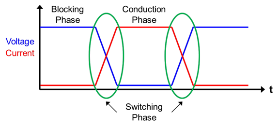 MOSFETs are required to block large voltages between their drain and source during switching.
During the blocking phase the MOSFET must withstand the full rated voltage of the application, while during the conduction and switching phases, losses and switching frequency are important. Conduction and switching losses both impact overall efficiency while higher switching frequencies enable smaller and lighter systems, a key attribute in both EVs and industrial applications.
The trend towards higher voltage is pushing the limits of the traditional silicon MOSFET. However, it is harder and costlier to get the low RDS(on) and high gate charge values required for reduced conduction losses and fast switching times. Power electronics designers are consequently turning to silicon carbide (SiC) to achieve higher efficiencies. SiC, a wide bandgap technology, has several advantages over silicon, including high thermal conductivity, a low thermal expansion coefficient, and high maximum current density, giving it excellent electrical conductivity compared to silicon. Additionally, SiC’s higher critical breakdown field means that a reduced thickness device can support a given voltage rating, leading to significant size reduction.
SiC MOSFETs are now available which can withstand voltage thresholds up to almost 10 kV, compared with 1500 V for the silicon variants. Also, the low switching losses and high operating frequencies of SiC devices enable them to achieve superior efficiencies, particularly in higher-power applications requiring high current, high temperatures, and high thermal conductivity.
onsemi Addresses the Need for Higher VoltagesIn response to the growing demand for devices with high breakdown voltages, onsemi has built an end-to-end in-house SiC manufacturing capability including a range of products such as SiC diodes, SiC MOSFETs, and SiC modules.
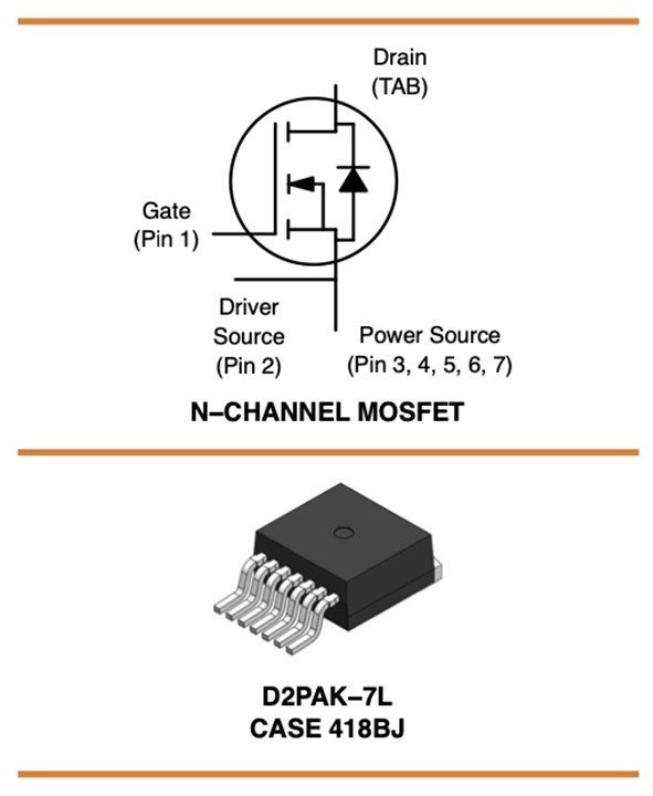
This product family includes the NTBG028N170M1, a high-breakdown voltage SiC MOSFET, figure 3. This N-channel, planar device is optimized for fast switching applications at high voltages, with a VDSS of 1700 V, and an extended VGS of ‑15/+25 V.
 onsemi’s NTBG028N170M1
The NTBG028N170M1 supports drain currents (ID) up to 71 A continuously and 195 A when pulsed and its superior RDS(ON) – typical value 28 mW – mitigates conduction losses. The ultra-low gate charge (QG(tot)), at just 222 nC, ensures low losses during high-frequency operation and the device is housed in a surface mountable D2PAK–7L package, which reduces parasitic effects during operation.
The onsemi EliteSiC range also includes a range of 1700 V-rated SiC Schottky diodes, which complement MOSFETs in power electronics systems such as rectifiers. The high Maximum Repetitive Peak Reverse Voltage (VRRM) of these diodes, along with their low Peak Forward voltage, (VFM) and excellent reverse leakage currents, equip design engineers to achieve stable, high voltage operation at elevated temperatures.
EliteSiC Supports Efficient Power Electronics DesignsThe quest for efficiency is relentless in applications which depend on power electronics devices. The trend towards higher system voltages is challenging the traditional Si-MOSFET and SiC devices offer a way forward, enhancing efficiencies while reducing form factors. The 1700 V NTBG028N170M1 from onsemi enables higher voltage designs for key power electronics systems.
The post Meeting the Demand for Higher Voltage Power Electronics appeared first on ELE Times.
Circuit to Success: Navigating a Career in ESDM as a New Grad
Author: Dr Abhilasha Gaur, Chief Operating Officer, Electronics Sector Skills Council of India (ESSCI)
As the last pages of the Class 12 exam papers are turned, a new chapter eagerly awaits the young minds of India. Amidst the excitement and anticipation of what lies ahead, many students find themselves pondering the age-old question: “What next?” For those with a passion for fashion, creativity, and innovation, the ESDM sector beckons as a realm of boundless opportunities. In this article, we embark on a journey through the colourful landscape of India’s ESDM industry, exploring the diverse career avenues that await aspiring professionals post-Class 12 exams.
 Dr Abhilasha Gaur, Chief Operating Officer, ESSCI
Exploring the Landscape:
The Electronics System Design and Manufacturing (ESDM) sector in India is experiencing phenomenal growth. Supported by government initiatives like “Make in India,” it’s rapidly becoming a major hub for electronics manufacturing and innovation. As per Invest India report, it is projected that India will achieve the milestone of becoming a $1 trillion digital economy by the fiscal year 2026. Presently, the electronics market within India holds a value of $155 billion, with domestic production contributing to 65% of this figure.
If you’ve completed your 12th standard and have a passion for technology, a career in the ESDM sector holds immense potential. ESDM encompasses the entire spectrum of electronics activities, including:
- Design: Designing integrated circuits (ICs), printed circuit boards (PCBs), electronic systems, and embedded software.
- Manufacturing: Production and assembly of electronic components, devices, and end-products. This includes semiconductor fabrication.
- Testing and Validation: Ensuring product quality, reliability, and compliance with industry standards.
- Repair and Maintenance: Servicing, troubleshooting, and repairing electronic products and systems.
Why is ESDM a Lucrative Career Path?
- Government Initiatives: The Government of India is heavily invested in developing the ESDM sector. Several policies and schemes aim to boost domestic manufacturing, attract foreign investment, and create a skilled workforce.
- Rapid Growth: India’s ESDM market is experiencing substantial growth, projected to reach trillions of rupees in value over the next few years. This growth fuels the demand for skilled professionals.
- Skill Development Focus: Programs focusing on skilling and training the ESDM workforce are a priority, ensuring you have ample opportunities to acquire the required skills.
- Diverse Ecosystem: India’s ESDM sector is diverse, offering opportunities in consumer electronics, telecommunications, defence, healthcare, automotive, and many other industries.
- Global Requirements: In the global market, the requirements of the ESDM industry are multifaceted and continually evolving. First and foremost, there is a persistent need for innovation and technological advancement to stay competitive. Companies are investing in research and development to create cutting-edge products that meet the ever-changing demands of consumers worldwide.
Next Level Options in ESDM for 12th Pass Students
Here’s how you can embark on a rewarding ESDM career after completing your 12th standard:
- Diploma Programs
- The ESDM sector offers exciting career opportunities for 12th graders through diploma programs. Options like Electronics and Communication Engineering (ECE) provide a strong foundation in electronics principles, communication systems, and embedded systems, opening doors to technician, engineer, and quality control roles. Electronics & Communication Engineering (ECE) focuses on telecom infrastructure and equipment, preparing individuals for technician and maintenance positions in this growing field. Consider your interests and career goals when choosing a diploma program to launch your journey in the dynamic ESDM sector.
- Skill Development and Certification Courses
- The booming ESDM sector demands skilled professionals. Skill development and certification courses offer a fast-track entry point, equipping 12th-pass students with industry-relevant skills. Government initiatives and industry collaborations provide various affordable options, empowering individuals to join the electronics revolution and contribute to India’s technological advancement. You can learn a lot of the basics and advanced skills with ESSCI – Electronics Sector Skills Council of India, a non-profit organisation, which works under the aegis of MSDE – Ministry of Skill Development and Entrepreneurship.
- Bachelor’s degree Options
If you desire advanced positions and specialization, consider bachelor’s degree courses. Some popular undergraduate courses are – B.Tech /B.E. in Electronics and Communication Engineering, Electrical and Electronics Engineering, Instrumentation and Control Engineering, Computer Science and Engineering, Mechatronics, Automation and Robotics. These engineering programs provide extensive training in electronics hardware design, testing, manufacturing processes, software skills, and embedded systems. Reputed institutes like IITs, NITs, IIITs and private colleges offer ESDM-focused bachelor’s degree courses for students interested in building careers in the electronics industry. The programs aim to develop competent engineering graduates equipped for upcoming technology shifts like IoT, AI and Industry 4.0.
Target Industries Within the ESDM Ecosystem
- Consumer Electronics Manufacturing: Contribute to the production of smartphones, laptops, televisions, home appliances, and other consumer goods.
- Semiconductors: Play a part in the design and fabrication of the integrated circuits that power these electronics.
- Telecom Infrastructure: Work on the networks and equipment that form the backbone of communication.
- Medical Devices and Healthcare: Develop life-saving medical electronics, diagnostic equipment, and healthcare technology.
- Defence and Aerospace: Be involved with electronics for military and space applications.
- Mechatronics: Design control systems, sensors, and smart features for vehicles.
Essential Skills for the ESDM Sector
- Technical Knowledge: Strong foundation in electronics fundamentals.
- Problem Solving: Analytical thinking and troubleshooting ability.
- Attention to Detail: Precision is critical when working with electronics.
- Adaptability: Keeping up with advancements in technology.
The post Circuit to Success: Navigating a Career in ESDM as a New Grad appeared first on ELE Times.
OMNIVISION Announces Automotive Image Sensor with TheiaCel Technology Now Compatible with NVIDIA Omniverse for Autonomous Driving Development
The post OMNIVISION Announces Automotive Image Sensor with TheiaCel Technology Now Compatible with NVIDIA Omniverse for Autonomous Driving Development appeared first on ELE Times.
Separating the Signal from the Noise: Combining Advanced Imaging with AI for Chip Defect Review
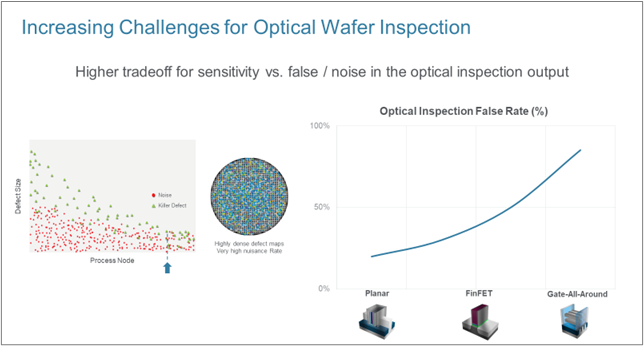
As the semiconductor industry moves to next-generation 3D architectures, the need intensifies for process control solutions that can reduce the time to ramp a technology to production-level yields. Gate-All-Around (GAA) transistors, EUV lithography, and scaled memory devices all present challenging requirements for detection of defects buried within 3D structures. As critical dimensions shrink, these defects can approach single-digit nanometers in size, or only a few atoms thick.
Chipmakers use two tools to find and control manufacturing defects: optical inspection to detect potential defects on the wafer, followed by eBeam review to characterize these defects in more precise detail. Optical inspection and eBeam review are complementary – together they deliver an actionable pareto that engineers can use to optimize yield and ensure faster time-to-market.
A key challenge facing eBeam defect review at the most advanced nodes is the ability to differentiate the true defects from the false alarms presented from the optical inspection systems, while maintaining the high throughput necessary for volume production.
The eBeam review process has become much more challenging as transistors have moved from planar to FinFET and now GAA. The “false rate” – when optical inspection flags something that is not a true defect – more than doubles with the GAA structures. Defects are smaller and killer defects are more difficult to distinguish from noise with GAA and advanced memories. The defect maps created after optical inspection become denser, with a large amount of nuisance (>90%), in order to capture the required defects of interest (DOIs). With such a high nuisance rate, it becomes nearly impossible to deliver an actionable pareto with enough DOIs to achieve statistically significant process control. To compensate for the high number of candidates in inspection, process control engineers need defect review systems that can deliver far more samples than today’s typical benchmark of several hundreds of DOI candidates.
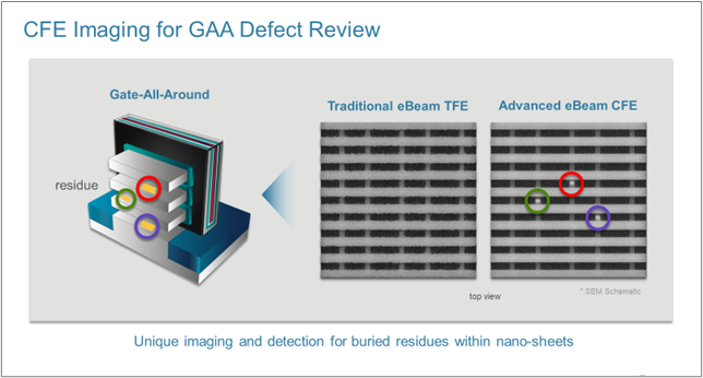
Applied Materials is the leading provider of eBeam defect review systems. In 2022, we introduced our “cold field emission” (CFE) technology, a breakthrough in eBeam imaging that enables chipmakers to better detect and image nanometer-scale, buried defects. We are now extending this technology to address the increased sampling requirements of the high false alarm rates (“High FAR”) of advanced logic and memory.
When combined with the use of back-scattered electrons that enable high-resolution imaging of deep structures, CFE technology allows better throughput while maintaining high sensitivity and resolution compared with previous-generation thermal field emission (TFE) sources – enabling sub-nanometer resolution for detecting the smallest buried defects.
Applied is now combining the use of CFE with deep learning AI technology for automatic extraction of true DOIs from the false “nuisance” defects. In many cases, the actual DOIs are only 5 percent or less of the review candidates. The deep learning network is continuously trained with data from the fab and sorts the defects into a defect distribution including voids, residues, scratches, particles and dozens of other defect types. Defect extraction is highly accurate, with nearly 100-percent accuracy.
3D Devices Need 3D Process ControlThe use of Applied-developed AI to enable automatic DOI extraction and classification is a new application. In one use case, the eBeam system considered roughly 10,000 defect candidates of a GAA device. While traditional defect review might be able to sample this many candidates, the new CFE with AI defect review system delivers much greater sensitivity and higher throughput, handling 10,000 candidates in less than an hour. Moreover, the AI-enabled in-line detection, filtering and classification system can classify 4X as many DOIs into specific types. Combining CFE technology with a full envelope of AI solutions makes it possible to deal with the high false alarm rates for 3D structures presented by the wafer inspection systems. CFE offers the required sensitivity to image the challenging defects, at higher throughputs compared with traditional TFE systems. Subsequently, with the help of AI, the required DOIs are captured with high accuracy, filtering out nuisances.
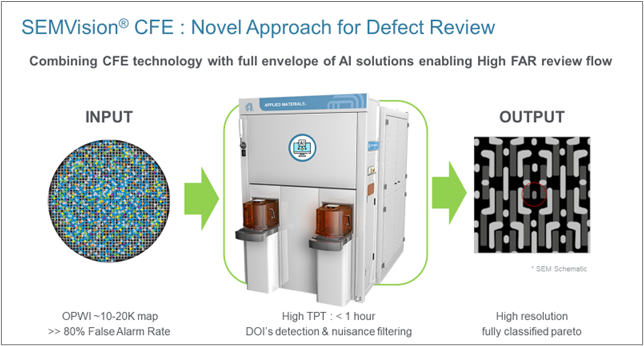
As 3D devices are being deployed in production, Applied has developed defect review technology that can sample 10,000 – 20,000 locations per hour, handle false-alarm rates exceeding 90 percent, and classify the defect types presented to statistical process control solutions. This innovative defect review approach is being successfully demonstrated at leading logic and memory chipmakers. Based on the feedback so far, we see a strong pull from customers as they address the High FAR challenge.
 SARVESH MUNDRA
Senior Product Marketing Manager
Applied Materials
The post Separating the Signal from the Noise: Combining Advanced Imaging with AI for Chip Defect Review appeared first on ELE Times.
Battery monitor maximizes performance of electric vehicle batteries
Courtesy: Arrow Electronics
Lithium-ion (Li-Ion) batteries are a common energy storage method for electric vehicles, offering very high energy density compared to all existing battery technologies. However, to maximize performance, it is essential to use a battery monitoring system (BMS) to safely manage the charging and discharging cycles, thereby extending the battery’s lifespan. This article will introduce the architecture and operation modes of BMS, as well as the product features and advantages of the BMS devices introduced by ADI.
BMS can enhance the operational efficiency of electric vehicle batteries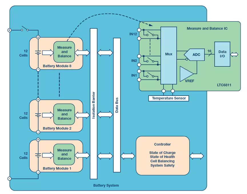
Advanced BMS can assist electric vehicles in efficiently extracting a significant amount of charge from the battery pack during operation. It can accurately measure the battery’s state of charge (SOC) to extend battery runtime or reduce weight, and enhance battery safety involves avoiding electrical overloads in the form of deep discharge, overcharging, overcurrent, and thermal overstress.
The primary function of the BMS is to monitor the physical parameters during battery operation, ensuring that each individual cell within the battery pack stays within its safe operating area (SOA). It monitors the charging and discharging currents, individual cell voltages, and the overall battery pack temperature. Based on these values, it not only ensures the safe operation of the battery but also facilitates SOC and state of health (SOH) calculations.
Another crucial function provided by the BMS is cell balancing. In a battery pack, individual cells may be connected in parallel or series to achieve the desired capacity and operating voltage (up to 1 kV or higher). Battery manufacturers attempt to provide identical cells for the battery pack, but achieving perfect uniformity is not physically realistic. Even small differences can lead to variations in charging or discharging levels, and the weakest cell in the battery pack can significantly impact the overall performance. Precise cell balancing is a vital feature of the BMS, ensuring the safe operation of the battery system at its maximum capacity.
Wireless BMS removes communication wiring, reducing complexityElectric vehicle batteries are composed of several cells connected in series. A typical battery pack, with 96 cells in series, generates over 400 V when charged at 4.2 V. The more cells in the battery pack, the higher the voltage achieved. While the charging and discharging currents are the same for all cells, it is necessary to monitor the voltage on each cell.
To accommodate the large number of batteries required for high-power automotive systems, multiple battery cells are often divided into several modules and distributed throughout the entire available space in the vehicle. A typical module consists of 10 to 24 cells and can be assembled in different configurations to fit various vehicle platforms. Modular design serves as the foundation for large battery packs, allowing the battery pack to be distributed over a larger area, thus optimizing space utilization more effectively.
In order to support a distributed modular topology in the high EMI environment of electric/hybrid vehicles, a robust communication system is essential. Isolated CAN bus is suitable for interconnecting modules in this environment. While the CAN bus provides a comprehensive network for interconnecting battery modules in automotive applications, it requires many additional components, leading to increased costs and circuit board space. Moreover, if modern Battery Management Systems (BMS) adopt wired connections, it comes with significant drawbacks. Wiring becomes a challenging issue as wires need to be routed to different modules, adding weight and complexity. Wires are also prone to pick up noise, requiring additional filtering.
Wireless BMS is a novel architecture that eliminates the need for communication wiring. In a wireless BMS, interconnection between each module is achieved through wireless connections. The wireless connection in large battery packs with multiple cells reduces wiring complexity, lowers weight, decreases costs, and enhances safety and reliability. However, wireless communication faces challenges in harsh EMI environments and signal propagation obstacles caused by RF-shielding metal components.
The SmartMesh embedded wireless network, introduced by ADI, has undergone on-site validation in Industrial Internet of Things (IoT) applications. It achieves redundancy through the use of path and frequency diversity, providing connections with reliability exceeding 99.999% in challenging environments such as industrial and automotive settings.
In addition to enhancing reliability by creating multiple redundant connection points, wireless mesh networks also extend the functionalities of BMS. The SmartMesh wireless network enables flexible placement of battery modules and improves the calculation of battery SOC and SOH. This is achieved by collecting more data from sensors installed in locations previously unsuitable for wiring. SmartMesh also provides time-correlated measurement results from each node, enabling more precise data collection.
ADI has integrated the LTC6811 battery stack monitor with ADI SmartMesh network technology, representing a significant breakthrough. This integration holds the potential to enhance the reliability of large multi-cell battery packs in electric and hybrid vehicles while reducing costs, weight, and wiring complexity.
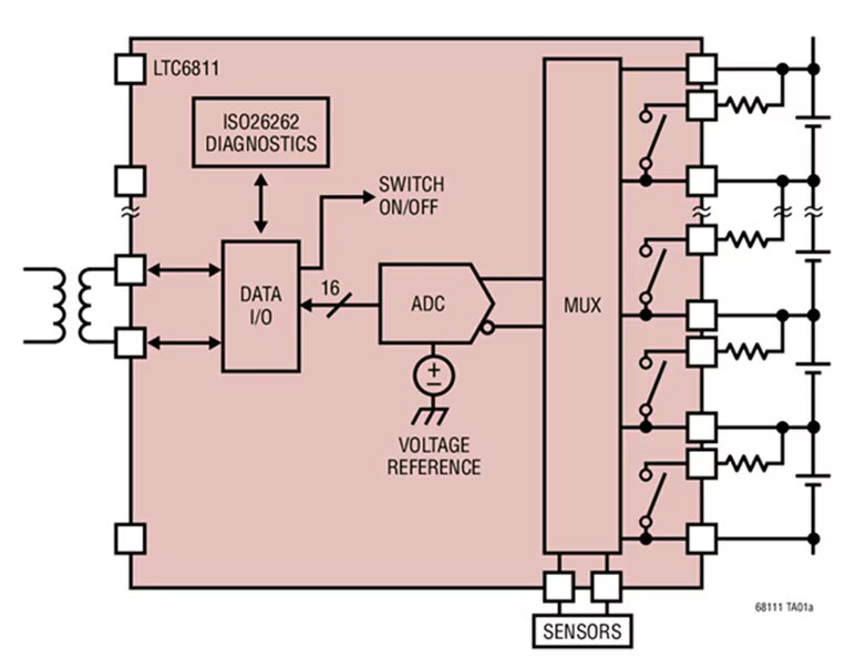
The LTC6811 is a battery stack monitor designed for multi-cell battery applications. It can measure the voltage of up to 12 series-connected cells with a total measurement error of less than 1.2mV. The measurement of all 12 cells can be completed within 290μs, and a lower data acquisition rate can be selected for high noise reduction. The LTC6811 has a battery measurement range of 0V to 5V, suitable for most battery chemistry applications. Multiple devices can be daisy-chained to simultaneously monitor very long high-voltage battery stacks. The device includes passive balancing for each cell, and data exchange occurs on either side of an isolation barrier, compiled by the system controller. The controller is responsible for calculating SOC, controlling battery balancing, checking SOH, and ensuring the entire system stays within safe limits.
Moreover, multiple LTC6811 devices can be daisy-chained, allowing simultaneous monitoring of long high-voltage battery stacks. Each LTC6811 has an isoSPI interface for high-speed and RF-resistant remote communication. When using LTC6811-1, multiple devices are connected in a daisy-chain, and all devices share one host processor connection. When using LTC6811-2, multiple devices are connected in parallel to the host processor, and each device is individually addressed.
The LTC6811 can be powered directly from the battery pack or an isolated power source and features passive balancing for each battery cell, along with individual PWM duty cycle control for each cell. Other features include a built-in 5V regulator, 5 general-purpose I/O lines, and a sleep mode (where current consumption is reduced to 4μA).
Cell balancing has a significant impact on the performance of batteries because even with precise manufacturing and selection, subtle differences can emerge between them. Any capacity mismatch between cells can lead to a reduction in the overall capacity of the battery pack. Clearly, the weakest cell in the stack will dominate the performance of the entire battery pack. Cell balancing is a technique that helps overcome this issue by equalizing the voltage and SOC between cells when the battery is fully charged.
Cell balancing technology can be divided into passive and active types. When using passive balancing, if one cell is overcharged, the excess charge is dissipated into a resistor. Typically, a shunt circuit is employed, consisting of a resistor and a power MOSFET used as a switch. When the cell is overcharged, the MOSFET is closed, dissipating the excess energy into the resistor. LTC6811 uses a built-in MOSFET to control the charging current for each monitored cell, thus balancing each cell being monitored. The integrated MOSFET allows for a compact design and can meet a 60 mA current requirement. For higher charging currents, an external MOSFET can be used. The device also provides a timer to adjust the balancing time.
On the other hand, active balancing involves redistributing excess energy among other cells in the module. This approach allows for energy recovery and lower heat generation, but the disadvantage is that it requires a more complex hardware design.
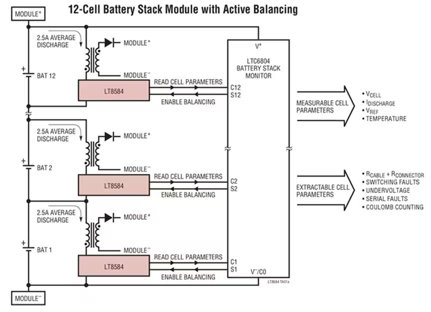
ADI has introduced an architecture using LT8584 to achieve active balancing of batteries. This architecture actively shunts charging current and returns energy to the battery pack, addressing the issues associated with passive shunt balancers. Energy is not dissipated as heat but is instead reused to recharge the remaining batteries in the stack. The architecture of this device also tackles a problem where one or more cells in the stack reach a low safe voltage threshold before the entire stack’s capacity is depleted, resulting in reduced runtime. Only active balancing can redistribute charge from stronger cells to weaker ones, allowing weaker cells to continue supplying power to the load and extracting a higher percentage of energy from the battery pack. The flyback topology enables charge to move back and forth between any two points in the battery pack. In most applications, the charge is returned to the battery module (12 cells or more), while in other applications, the charge is returned to the entire battery stack or auxiliary power rails.
The LT8584 is a monolithic flyback DC/DC converter designed specifically for active balancing of high-voltage battery packs. The high efficiency of the switch-mode regulator significantly increases the achievable balancing current while reducing heat dissipation. Additionally, active balancing allows for capacity recovery in stacks of mismatched batteries, a feature not attainable with passive balancing systems. In typical systems, over 99% of the total battery capacity can be achieved.
The LT8584 features an integrated 6A, 50V power switch, reducing the design complexity of the application circuit. The device operates entirely relying on the cells which it is discharging, eliminating the need for complex biasing schemes typically required when using an external power switches. The enable pin (DIN) is designed to seamlessly coordinate with the LTC680x series battery stack monitor ICs. Additionally, when used in conjunction with LTC680x series devices, the LT8584 provides system telemetry functions, including current and temperature monitoring. When disabled, the LT8584 typically consumes less than 20nA of total static current from the battery.
ConclusionThe key to low-emission vehicles lies in electrification, but it also requires smart management of energy sources (such as lithium-ion batteries). Improper management could render the battery pack unreliable, significantly reducing the safety of the vehicle. Both active and passive battery balancing contribute to safe and efficient battery management. Distributed battery modules are easy to support, and they can reliably transmit data to the BMS controller, whether through wired or wireless means, enabling dependable SOC and SOH calculations. ADI offers a comprehensive range of BMS components that can assist customers in accelerating BMS development, ensuring more efficient management of the operational efficiency and safety of electric vehicle batteries.
The post Battery monitor maximizes performance of electric vehicle batteries appeared first on ELE Times.
Passive components in EV chargers should be selected carefully (EV Charging)
Courtesy: Avnet
When selecting components for an EV charger design, semiconductors are the usual focus of attention. Newer power switching technologies, Silicon Carbide in particular, promise very low losses and overall cost savings. Passive components cannot be forgotten. The use of wide bandgap (WBG) switches such as SiC MOSFETs presents additional opportunities for optimization. Passive components in the power train can be smaller in size and lower in weight, which comes with reduced cost. These developments bring passive technologies into play that would otherwise be unsuitable. The main passives to consider are DC-link capacitors, filter inductors, and transformers.
The DC-link capacitorAll on- and off-board EV chargers have similar power chains. They start with a power factor correction (PFC) stage followed by an isolated DC-DC conversion stage. The output power level does not change this basic architecture, as the fastest 400kW+ roadside chargers will still typically comprise lower power modules in a stacked configuration. Each module will deliver around 30kW, to reduce stress and provide redundancy. Each stage may be bi-directional in modern designs and overall would resemble any high-power AC-DC converter.
A Typical EV charger outline with critical passive components highlighted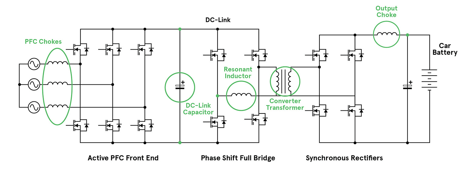 Passives play an important role in EV charging topologies. Their selection will depend on the type of converter used, which will help indicate the efficiencies that can be achieved through the most optimal component selection.
One of the main differences between a generic converter and an EV battery charger design is the sizing of the DC-link capacitor. This capacitor is positioned on the DC rail, or link, between the PFC and DC-DC conversion stages. The potential here will be a voltage of around 650V up to 1000V. In a general-purpose AC-DC converter, this capacitor is usually sized for ‘hold-up’ time, maintaining the rail for typically 18/20ms after a mains failure. At 30kW, this would need around 8,000 µF, occupying about 80 cubic inches (1300cm3). At this capacity, aluminum electrolytics are the most economically viable option.
Hold-up capacitance is calculated by equating the hold-up energy required (hold-up time x output power/efficiency), with the energy expended as the capacitor voltage drops after AC failure from its normal level to a drop-out level, perhaps from 650V to 500V. That is, 30kW x 20ms/0.90 = (0.5 x C x 6502) – (0.5 x C x 5002) giving C = 7.7 mF.
In an EV charger application, hold-up is not an issue. The size of the DC-link capacitor is based on its ability to source high-frequency ripple current for the DC-DC stage and sink ripple current from the PFC stage. The total ripple voltage and temperature rise will also be factors.
The most suitable part is determined by the Equivalent Series Resistance (ESR) and Equivalent Series Inductance (ESL) of the capacitor, as well as its capacitance. Although high capacitance for hold-up is not necessary it is still common to select AL-electrolytics. Often engineers will use large capacitors in parallel, to achieve the desired ESR and ESL. Because of the capacitors’ size, it can be difficult to keep total connection resistance low with good ripple current sharing between the components.
The total impedance of an AL-electrolytic will typically reach its minimum at around 10kHz. That frequency is due to the capacitance, ESL, and variation in ESR. This low frequency is not a good match when using WBG devices, which switch better at several hundred kHz. The ESR of AL-electrolytics also rises strongly at low temperatures which could be problematic at start-up, especially in a battery charger application located outside. At the other extreme, 105°C is usually the maximum rating for an AL electrolytic.
Transfer curve of an AL electrolytic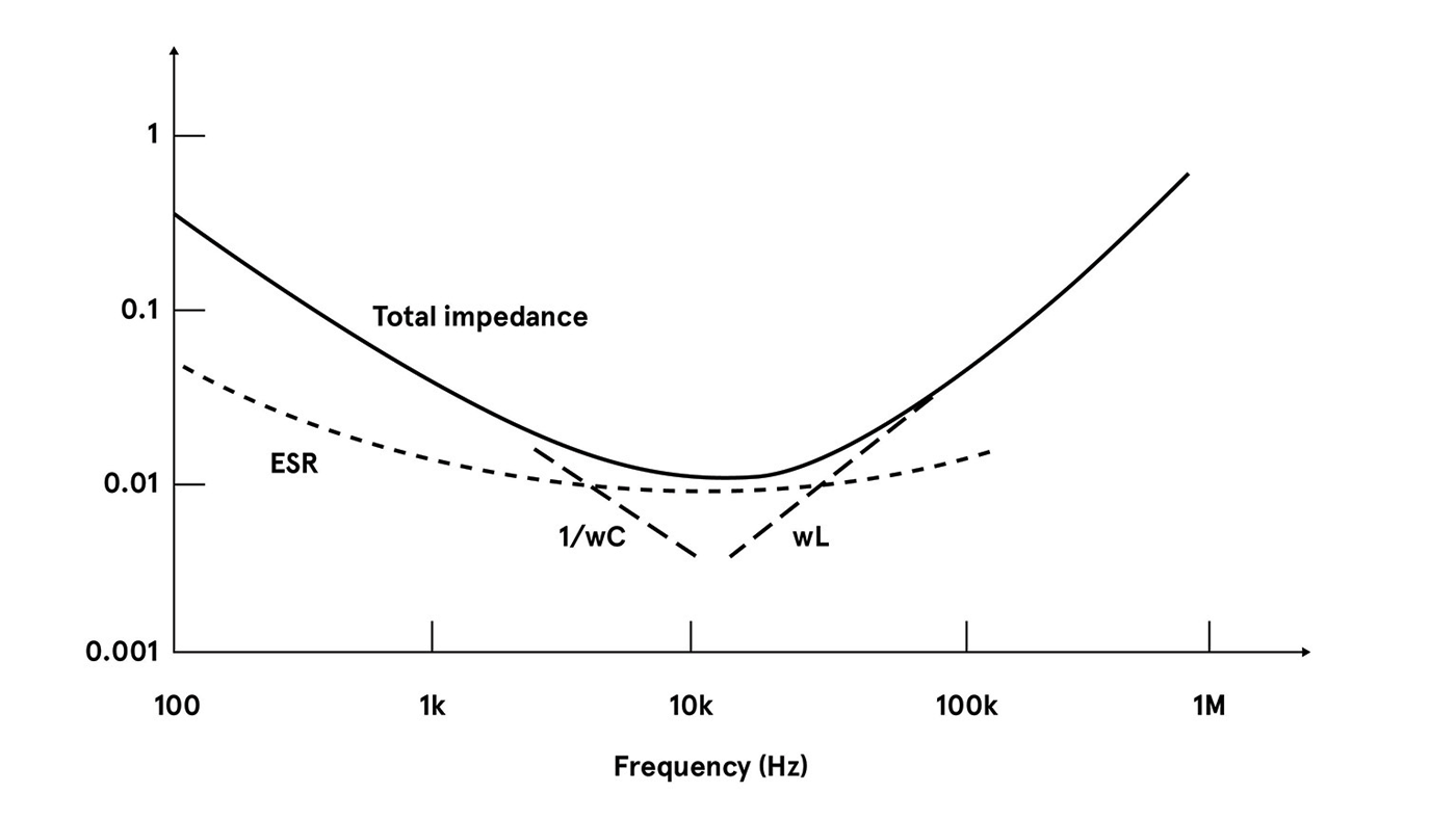 The impedance of a large AL-electrolytic capacitor is typically at a minimum around 10kHz, which is not a good fit when using wide bandgap power transistors.
For an alternative to AL-electrolytics, look at film and multilayer ceramic capacitors (MLCCs). MLCCs have very low ESR and ESL, so the low impedance point occurs at a higher frequency. This higher frequency is more suitable when using WBG devices. The MLCC also has a longer lifetime than AL-electrolytics, perhaps 10x under the same conditions.
It is now common to see film capacitors used in the DC-link position. Film types are available rated to high voltages and operate at temperatures of at least 135°C. The common PCB-mount ‘box’ format used for MLCCs makes them easy to assemble with good packing density. They can also self-heal after over-voltage stress, unlike AL-electrolytics.
However, MLCCs are relatively high cost and low capacitance value per package. Achieving high capacitance requires using many in parallel. Some MLCCs are also relatively fragile and susceptible to substrate flexing. However, some MLCCs designed specifically for DC-link applications are now available, with fitted metal frames around paralleled parts. This eases assembly and provides some mechanical flexibility in the terminations.
Quantifying ripple currentRipple current for a DC-link capacitor is difficult to quantify. The value depends on operating conditions, and summing the total value sunk from the PFC stage and sourced to the DC-DC stage is not simple. If the stages are not synchronized or if either stage is variable frequency, it is harder still to identify.
Simulation and bench measurements can be used, but as an approximation, for a DC link at 650V and 30kW load, the average current is about 50A allowing for inefficiencies. For a DC-DC duty cycle of 80%, this is about 25A rms sourced from the capacitor assuming a square wave. At a switching frequency of 100kHz and 10V rms ripple, only about 4µF would be needed if capacitive impedance dominates. If the capacitor ESR were 10 milliohms, this would add an extra 0.25V rms of ripple. We could guess that the ripple from the PFC stage is of the same order.
Despite these gross assumptions, it indicates that only a few tens of µF would be needed and film capacitors become practical if several are paralleled to achieve the ripple current capability. For example, four paralleled 20µF/700V metalized polypropylene capacitors can handle 62.5A rms total ripple with an overall ESR of less than one milliohm, giving less than 4 W total dissipation at 50A rms ripple current. The overall volume is 8.5 cubic inches (139 cm3).
An AL-electrolytic solution, for similar ripple current capability could be assembled from 10x 2700µF/400V parts, in a 5-parallel 2-series arrangement, with about 85A ripple current rating (10kHz) and an ESR of about 8 milliohms total. At 50A rms ripple current, this would give about 20W of dissipation overall.
Ripple voltage is much lower than the film capacitor solution, because of lower capacitive impedance, but the overall volume would be 125 cubic inches (2060 cm3) or nearly 15x larger. Further advantages of film capacitors include a particularly low ESL of a few tens of nH, adding only a volt or so to the ripple voltage waveform.
Comparing a typical MLCC solution, three in parallel could achieve 50A rms ripple rating and adequate capacitance for less than 10V rms ripple. ESR would be around 2 milliohms total and dissipation around 3W overall. Low ESR and ESL are maintained up to a frequency of at least 1MHz. This makes MLCC a good candidate for ultra-fast switching where capacitance value is less important. ESR and capacitance do vary however quite strongly with temperature and bias voltage. Typically, three modules would occupy just 0.8 cubic inches (13.25 cm3).
Indicative volume pricing shows four of the film parts would cost around one quarter the price of ten AL-electrolytics, while three MLCC modules would be about half the price of the ten AL-electrolytics. In practice, derating will be applied to capacitors of any type, requiring further parallel parts. That may apply more so for the electrolytics. In this case, the difference becomes even more striking. The table shows the difference in headline performance of film, MLCC, and AL-electrolytic capacitors.
Comparing capacitors for EV chargers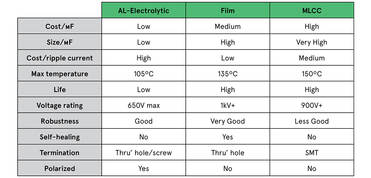 A comparison of capacitor technologies for typical industrial-grade parts, including the figures of merit important in an EV charging application.
Magnetics in EV chargers
A comparison of capacitor technologies for typical industrial-grade parts, including the figures of merit important in an EV charging application.
Magnetics in EV chargers
Magnetic components in EV chargers are like any found in AC-DC converters, but the fast charger environment and the trend toward WBG semiconductors influences the choice of fabrication technique. The main components to consider are the input EMI filter, PFC inductor, DC-DC transformer, output choke, and any additional resonant inductors, depending on the converter topology being used.
The EMI filter will comprise at least one common-mode choke in the AC input lines with windings phased so that flux from line currents cancel. This allows high inductance to be used without risk of saturation. High permeability ferrite cores are normally used but nano-crystalline material is sometimes seen for maximum inductance.
Windings are spaced to achieve voltage isolation and ideally in just a single layer, to keep self-capacitance low and self-resonance high. Differential-mode chokes are also usually necessary, and these see flux from the full line current. To avoid saturation, they are typically low inductance, wound on iron power core toroids. Some common-mode choke designs add separation to their windings to deliberately introduce leakage flux, which acts as an integrated differential mode choke. Both common-mode and differential-mode chokes are wound with magnet wire on bobbins or headers for PCB mounting.
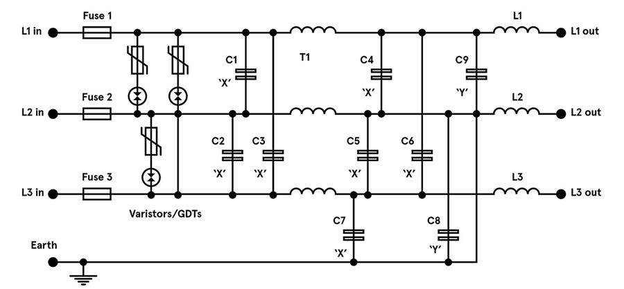 The operating environment will influence the choice of common-mode (T1) and differential-mode (L1, L2, L3) chokes in the EMI filter stage of an EV charger, based on the materials used and manufacturing process.
Magnetic component selection in EV chargers
The operating environment will influence the choice of common-mode (T1) and differential-mode (L1, L2, L3) chokes in the EMI filter stage of an EV charger, based on the materials used and manufacturing process.
Magnetic component selection in EV chargers
The PFC choke operates at high frequency and its inductance value is chosen to match the operating mode of the stage; continuous, discontinuous, or ‘boundary’. These modes trade off semiconductor stress with potential EMI and choke size, and with the high peak currents present, a low effective core permeability is needed to avoid saturation.
A powder core would produce excessive core losses, so the preference is a gapped ferrite. This should offer minimum loss at the working flux density and frequency, and at the expected operating temperature. The component could be of bobbin construction, but a planar approach can be practical with PCB traces used as windings, giving low losses and a large surface area to help dissipate heat.
The DC-DC converter topology will invariably be a version of a forward converter, typically a full-bridge, and often a resonant type at the power levels involved. Planar transformer designs are popular as they are consistent and easy to integrate with the power switches operating at high frequency. However, safety isolation is required and the appropriate creepage and clearance distances can be difficult to achieve with this construction.
In most cases, high primary inductance is needed, achieved with an ungapped high-permeability core, and, like the PFC choke, the material is chosen for the lowest core losses. Resonant converters use an extra inductor that can be formed from the leakage inductance of the main transformer. This can be difficult to control and can limit overall performance, so normally the inductor is a separate component. The value can be very low so it could conceivably be air-cored but is more likely to utilize a core to constrain the magnetic field and reduce interactions.
An output choke, if necessary for the topology, is chosen in a similar way to the PFC choke. A desired ripple current is specified, which sets inductance for a given output voltage, duty cycle, and frequency. The DC output current flows through the choke, so a gapped ferrite is the normal core solution. The component again could be a planar construction in modern designs.
ConclusionPassive components can become a limit to the performance achieved in EV charger designs. There are choices of components however which can leverage the characteristics of the latest semiconductor technologies to minimize losses and contribute to overall reduction in size, weight, and cost.
As a global leader in IP&E solutions, Avnet has a robust supplier line card in all regions as well as extensive design support and demand creation services. Our dedicated IP&E experts can help with everything from supply chain needs to service organization requirements.
The post Passive components in EV chargers should be selected carefully (EV Charging) appeared first on ELE Times.
Servotech Power Systems to Build 20 EV Charging Stations for Nashik Municipal Corporation
Servotech Power Systems Ltd., a prominent player in the EV charging and solar industry, has secured a substantial contract from the Nashik Municipal Corporation (NMC). This contract involves Servotech supplying, commissioning, and constructing 20 electric vehicle (EV) charging stations throughout the Nashik Municipal Corporation area.
The objective of this contract is to meet the increasing need for convenient and accessible charging facilities for electric vehicles, thus facilitating the state’s shift towards sustainable transportation solutions. As the demand for EV mobility grows, there is a corresponding need for enhanced EV charging infrastructure and these charging stations will enable EV owners to recharge their vehicles conveniently while on the move.
Servotech will oversee the installation, supply, commissioning, construction and maintenance of EV charging stations, catering to various vehicles and substantially improving Nashik’s EV charging network. This positions Servotech as a frontrunner in India’s growing EV infrastructure market and aligns with the government’s vision to create a robust EV ecosystem nationwide. Additionally, this initiative reflects Servotech’s commitment to sustainability by facilitating Nashik’s transition to cleaner transportation, aligning with its environmental responsibility goals, and reducing carbon emissions in one of the key cities of India.
Sarika Bhatia, Director of Servotech Power Systems Ltd. said, “This contract represents a major milestone for Servotech Power Systems, we are deeply committed to advancing India’s electric vehicle revolution and fostering sustainable transportation solutions. We are already a leader in the EV charger market and through this initiative, we are set to become a leader in the EV charging infrastructure market as well. This collaboration with the Nashik Municipal Corporation underscores our capabilities to provide cutting-edge and reliable EV charging solutions for cities across the nation. By expanding the accessibility of EV charging infrastructure, we aim to support the widespread adoption of electric vehicles, reducing carbon emissions and promoting a cleaner, greener future for generations to come. We are excited to contribute to Nashik’s transition to cleaner transportation and look forward to delivering high-quality charging solutions that meet the city’s evolving needs. As a premier EV charger manufacturer, we aim to transform India into a nation where EVs are not just a vision but a reality. With a shared vision and unwavering dedication, we believe in making this dream come true, driving a seamless shift toward a greener, more sustainable transportation landscape.
The post Servotech Power Systems to Build 20 EV Charging Stations for Nashik Municipal Corporation appeared first on ELE Times.
Powering the Next Wave of Smart Industrial Sensors with NuMicro M091 Series Microcontrollers
In the era of Industry 5.0, where intelligence, sensing capabilities, and automation are paramount, the demand for precise, compact sensors continues to soar across various fields of industrial automation and IoT applications—introducing the NuMicro M091 series, a line of 32-bit high-integration analog microcontrollers designed to elevate the accuracy of analog functions and digital controls within a small package size.
Key Features of High-Integration Analog Microcontrollers
Based on the Arm Cortex-M0 core, the NuMicro M091 series operates at frequencies up to 72 MHz, with Flash memory ranging from 32 KB to 64 KB, 8 KB of SRAM, and a working voltage of 2.7V to 3.6V. Breaking new ground in performance, this series offers rich analog peripherals, including 4 sets of 12-bit DACs and up to 16 channels of 12-bit 2 MSPS ADCs. Additionally, it supports up to four sets of precision Rail-to-Rail operational amplifiers (OP Amps), delivering exceptional specifications to enhance output signal accuracy. These specifications include Input Offset Voltage as low as 50 µV, an extremely low-temperature drift of 0.05 µV/℃, a high slew rate of up to 6V/µs, and a broad gain bandwidth of 8 MHz, ensuring the integrity of amplified signals. It also includes a built-in temperature sensor with a ± 2 °C deviation.
Rich Peripheral Modules and Applications
With the addition of up to 6 sets of 32-bit timers, 1 UART, 1 SPI, 2 I²C, and 6-channel 16-bit BPWM peripheral modules, the NuMicro M091 series ensures seamless adaptation to various application scenarios, providing a more comprehensive solution. To meet the growing demand for small-sized sensors, this series offers QFN33 (4 x 4 mm) and QFN48 (5 x 5 mm) compact package sizes, facilitating easy integration of sensing technology into diverse application scenarios.
Ease of Development
Equipped with the NuMaker-M091YD development board and Nu-Link debugger, the M091 series offers powerful tools for product evaluation and development. Moreover, it supports third-party IDEs such as Keil MDK, IAR EWARM, and the self-developed NuEclipse IDE by Nuvoton, providing developers with more choices and convenience.
Experience the Future of Industrial Sensing with NuMicro M091 Series Microcontrollers, Redefining Precision, and Integration in the World of Smart Sensors.
The post Powering the Next Wave of Smart Industrial Sensors with NuMicro M091 Series Microcontrollers appeared first on ELE Times.
Infineon partner Thistle Technologies integrates its Verified Boot technology with Infineon’s OPTIGA Trust M for enhanced device security
Infineon Technologies AG has announced the integration of its OPTIGA Trust M security controller, with tamper-resistant hardware certified to Common Criteria EAL6+, with the Verified Boot technology by Thistle Technologies, a pioneer of advanced security solutions for connected devices. This integration enables designers to easily defend their devices against firmware tampering and protect the software supply chain integrity. The result is improved end-user security, which is particularly important in industries with high security requirements such as healthcare, automotive and device manufacturing.
Thistle Technologies Verified Boot provides a secured boot process for IoT devices. Enhanced integrity checks cryptographically examine that the device firmware has not been tampered with. The solution supports the needs of a wide range of IoT devices for smart homes, smart cities and smart buildings, among others, enabling easy implementation with minimal development time. By leveraging the robust security features of Infineon’s OPTIGA Trust M, including its hardware-based root-of-trust, the technology offers a high level of protection against unauthorized firmware modifications and sophisticated cyberattacks.
“Since the start of our partnership in January 2023, Thistle has developed a software integration for our OPTIGA Trust M within Linux to extend our hardware capability into the application software domain for Linux-based system architectures,” said Vijayaraghavan Narayanan, Senior Director and Head of Edge Identity & Authentication at Infineon. “The new solution enables our shared customers to quickly enhance the security of their development.”
“Integrating our Verified Boot technology with Infineon’s OPTIGA Trust M is a significant step forward in making it easy to incorporate sophisticated security capabilities into devices quickly,” said Window Snyder, CEO of Thistle Technologies.
The post Infineon partner Thistle Technologies integrates its Verified Boot technology with Infineon’s OPTIGA Trust M for enhanced device security appeared first on ELE Times.
Infineon sues Innoscience for Patent Infringement
Infineon Technologies AG has filed a lawsuit, through its subsidiary Infineon Technologies Austria AG, against Innoscience (Zhuhai) Technology Company, Ltd., and Innoscience America, Inc. and affiliates (hereinafter: Innoscience). Infineon is seeking a permanent injunction for infringement of a United States patent relating to gallium nitride (GaN) technology owned by Infineon. The patent claims cover core aspects of GaN power semiconductors encompassing innovations that enable the reliability and performance of Infineon’s proprietary GaN devices. The lawsuit was filed in the district court of the Central District of California.
Infineon alleges that Innoscience infringes the Infineon patent mentioned above by making, using, selling, offering to sell and/or importing into the United States various products, including GaN transistors for numerous applications, within automotive, data centres, solar, motor drives, consumer electronics, and related products used in automotive, industrial, and commercial applications.
“The production of gallium nitride power transistors requires completely new semiconductor designs and processes”, said Adam White, President of Infineon’s Power & Sensor Systems Division. “With nearly two decades of GaN experience, Infineon can guarantee the outstanding quality required for the highest performance in the respective end products. We vigorously protect our intellectual property and thus act in the interest of all customers and end users.” Infineon has been investing in R&D, product development and manufacturing expertise related to GaN technology for decades. Infineon continues to defend its intellectual property and protect its investments.
On 24 October 2023, Infineon announced the closing of the acquisition of GaN Systems Inc., becoming a leading GaN powerhouse and further expanding its leading position in power semiconductors. Infineon leads the industry with its GaN patent portfolio, comprising around 350 patent families. Market analysts expect the GaN revenue for power applications to grow by 49% CAGR to approximately US$2 billion by 2028 (source: Yole, Power SiC and GaN Compound Semiconductor Market Monitor Q4 2023). Gallium nitride is a wide bandgap semiconductor with superior switching performance that allows smaller size, higher efficiency and lower-cost power systems.
The post Infineon sues Innoscience for Patent Infringement appeared first on ELE Times.
Infineon’s new CoolSiC MOSFETs 2000 V offer increased power density without compromising system reliability
Infineon Technologies AG introduces the new CoolSiC MOSFETs 2000 V in the TO-247PLUS-4-HCC package to meet designers’ demand for increased power density without compromising the system’s reliability even under demanding high voltage and switching frequency conditions. The CoolSiC MOSFETs offer a higher DC link voltage so that the power can be increased without increasing the current. It is the first discrete silicon carbide device with a breakdown voltage of 2000 V on the market and comes in a TO-247PLUS-4-HCC package with a creepage distance of 14 mm and a clearance distance of 5.4 mm. With low switching losses, the devices are ideal for solar (e.g. string inverters) as well as energy storage systems and electric vehicle charging applications.
The CoolSiC MOSFET 2000 V product family is ideally suited for high DC link systems with up to 1500 VDC. Compared to 1700 V SiC MOSFETs, the devices also provide a sufficiently high overvoltage margin for 1500 VDC systems. The CoolSiC MOSFETs deliver a benchmark gate threshold voltage of 4.5 V and are equipped with a robust body diode for hard commutation. Due to the .XT connection technology, the components offer first-class thermal performance. They are also highly resistant to humidity.
In addition to the CoolSiC MOSFETs 2000 V, Infineon will soon be launching the matching CoolSiC diodes: The first launch will be the 2000 V diode portfolio in the TO-247PLUS 4-pin package in the third quarter of 2024, followed by the 2000 V CoolSiC diode portfolio in the TO-247-2 package in the final quarter of 2024. These diodes are particularly suitable for solar applications. A matching gate driver portfolio is also available.
The post Infineon’s new CoolSiC MOSFETs 2000 V offer increased power density without compromising system reliability appeared first on ELE Times.
Infineon sets new industry standard for enhanced power density and efficiency with OptiMOS 6 200 V MOSFETs
Motor drive applications are taking a leap forward with the launch of the Infineon Technologies AG OptiMOS 6 200 V MOSFET product family. The new portfolio is designed to deliver optimal performance in applications such as e-scooters, micro-EVs, and E-forklifts. The improved conduction losses and switching behaviour for these new MOSFETs reduce the electromagnetic interference (EMI) and switching losses. This benefits various switching applications, including servers, telecom, energy storage systems (ESS), audio, solar and others. Additionally, the combination of a wide safe operating area (SOA) and industry-leading RDS(on) results in a perfect fit for static switching applications such as battery management systems. With the introduction of the new OptiMOS 6 200 V product family, Infineon sets a new industry benchmark with increased power density, efficiency, and system reliability for its customers’ benefit.
The OptiMOS 6 200 V portfolio delivers enhanced technical features compared to its predecessor, the OptiMOS 3. It features a 42 per cent lower RDS(on) that contributes to reduced conduction losses and increased output power. Regarding diode behaviour, the OptiMOS 6 200 V provides a significant increase in softness, more than three times that of the OptiMOS 3. Combined with up to 89 per cent reduction in Qrr(typ), the switching and EMI behaviours are significantly improved. The technology also features improvements in parasitic capacitance linearity (Coss and Crss), which reduces oscillation during switching and lowers voltage overshoot. A tighter VGS(th) spread and lower transconductance aid in MOSFET paralleling and current sharing, leading to more uniform temperatures and reducing the number of paralleled MOSFETs.
The OptiMOS 6 200 V products feature an improved SOA and are classified as MSL 1 according to J-STD-020. These RoHS-compliant, lead-free products align with current industry standards.
The post Infineon sets new industry standard for enhanced power density and efficiency with OptiMOS 6 200 V MOSFETs appeared first on ELE Times.
Vishay Intertechnology Upgrades TFBS4xx and TFDU4xx Series IR Transceiver Modules With Longer Link Distance and Improved ESD Robustness
Offering Drop-in Replacements for Existing Solutions, IrDA-Compliant Devices Feature New In-House IC and Surface Emitter Chip Technology
Vishay Intertechnology, Inc. has announced that it has upgraded its TFBS4xx and TFDU4xx series of infrared (IR) transceiver modules for IrDA applications to offer 20 % longer link distance and improved ESD robustness to 2 kV. With support for data rates up to 115.2 kbit/s (SIR) and link distances of 1 meter, the devices are intended for wireless communication and data transmission in energy meters and monitors, industrial automation controls, mobile phones, and medical equipment. To increase battery life in portable devices, the modules offer low power consumption with an idle supply current of < 70 μA, down to < 1 μA in shutdown mode.
Devices in the Vishay Semiconductors TFBS4xxx and TFDU4xxx series each consist of a PIN photodiode, infrared emitter (IRED), and low-power control IC in a single package. By upgrading the IR transceivers with Vishay’s latest in-house IC and surface emitter chip technology, the company is assuring the long-term availability of IRDC products for its customers. As drop-in replacements for existing devices, the modules help save costs by eliminating the need for PCB redesigns.
Compliant with the latest IrDA physical layer specification, TFBS4xxx and TFDU4xxx series devices are backwards-compatible and are offered in top- and side-view surface-mount packages. The enhanced solutions provide drop-in, plug-and-play replacements for existing devices in the series.
RoHS-compliant, halogen-free, and Vishay Green, the devices are offered in a variety of package sizes and feature a wide operating voltage range from 2.4 V to 5.5 V and an operating temperature range from -25 °C to +85 °C.
Device Specification Table:
| Part # | Dimensions (mm) |
| TFBS4650 | 1.6 by 6.8 by 2.8 |
| TFBS4652 | 1.6 by 6.8 by 2.8 |
| TFBS4711 | 1.9 by 6 by 3 |
| TFDU4101 | 4 by 9.7 by 4.7 |
| TFDU4301 | 3.1 by 8.5 by 2.5 |
The post Vishay Intertechnology Upgrades TFBS4xx and TFDU4xx Series IR Transceiver Modules With Longer Link Distance and Improved ESD Robustness appeared first on ELE Times.
Cerebras and G42 Break Ground on Condor Galaxy 3, an 8 exaFLOPs AI Supercomputer
Featuring 64 Cerebras CS-3 Systems, Condor Galaxy 3 Doubles Performance at Same Power and Cost
Cerebras Systems, the pioneer in accelerating generative AI, and G42, the Abu Dhabi-based leading technology holding group, today announced the build of Condor Galaxy 3 (CG-3), the third cluster of their constellation of AI supercomputers, the Condor Galaxy. Featuring 64 of Cerebras’ newly announced CS-3 systems – all powered by the industry’s fastest AI chip, the Wafer-Scale Engine 3 (WSE-3) – Condor Galaxy 3 will deliver 8 exaFLOPs of AI with 58 million AI-optimized cores.
The Cerebras and G42 strategic partnership already delivered 8 exaFLOPs of AI supercomputing performance via Condor Galaxy 1 and Condor Galaxy 2, each amongst the largest AI supercomputers in the world. Located in Dallas, Texas, Condor Galaxy 3 brings the current total of the Condor Galaxy network to 16 exaFLOPs.
“With Condor Galaxy 3, we continue to achieve our joint vision of transforming the worldwide inventory of AI computing through the development of the world’s largest and fastest AI supercomputers,” said Kiril Evtimov, Group CTO of G42. “The existing Condor Galaxy network has trained some of the leading open-source models in the industry, with tens of thousands of downloads. By doubling the capacity to 16 exaFLOPs, we look forward to seeing the next wave of innovation Condor Galaxy supercomputers can enable.”
At the heart of Condor Galaxy 3 are 64 Cerebras CS-3 Systems. Each CS-3 is powered by the new 4 trillion transistor, 900,000 AI core WSE-3. Manufactured at TSMC at the 5-nanometer node, the WSE-3 delivers twice the performance at the same power and for the same price as the previous generation part. Purpose-built for training the industry’s largest AI models, WSE-3 delivers an astounding 125 petaflops of peak AI performance per chip.
“We are proud that our newly announced CS-3 systems will play a critical role in our pioneering strategic partnership with G42,” said Andrew Feldman, CEO and co-founder of Cerebras. “Condor Galaxy 3 and the follow-on supercomputers, will together deliver tens of exaflops of AI compute This marks a significant milestone in AI computing, providing unparalleled processing power and efficiency.”
Condor Galaxy has trained state-of-the-art industry-leading generative AI models, including Jais-30B, Med42, Crystal-Coder-7B and BTLM-3B-8K. Jais 13B and Jais30B are the best bilingual Arabic models in the world, now available on Azure Cloud. BTLM-3B-8K is the number one leading 3B model on HuggingFace, offering 7B parameter performance in a light 3B parameter model for inference. Med42, developed with M42 and Core42, is a leading clinical LLM, trained on Condor Galaxy 1 in a weekend and surpassing MedPaLM on performance and accuracy.
The post Cerebras and G42 Break Ground on Condor Galaxy 3, an 8 exaFLOPs AI Supercomputer appeared first on ELE Times.
Cerebras Systems Unveils World’s Fastest AI Chip with Whopping 4 Trillion Transistors
Third Generation 5nm Wafer Scale Engine (WSE-3) Powers Industry’s Most Scalable AI Supercomputers, Up To 256 exaFLOPs via 2048 Nodes
Cerebras Systems, the pioneer in accelerating generative AI, has doubled down on its existing world record of fastest AI chip with the introduction of the Wafer Scale Engine 3. The WSE-3 delivers twice the performance of the previous record-holder, the Cerebras WSE-2, at the same power draw and for the same price. Purpose built for training the industry’s largest AI models, the 5nm-based, 4 trillion transistor WSE-3 powers the Cerebras CS-3 AI supercomputer, delivering 125 petaflops of peak AI performance through 900,000 AI optimized compute cores.
Key Specs:
- 4 trillion transistors
- 900,000 AI cores
- 125 petaflops of peak AI performance
- 44GB on-chip SRAM
- 5nm TSMC process
- External memory: 1.5TB, 12TB, or 1.2PB
- Trains AI models up to 24 trillion parameters
- Cluster size of up to 2048 CS-3 systems
With a huge memory system of up to 1.2 petabytes, the CS-3 is designed to train next generation frontier models 10x larger than GPT-4 and Gemini. 24 trillion parameter models can be stored in a single logical memory space without partitioning or refactoring, dramatically simplifying training workflow and accelerating developer productivity. Training a one-trillion parameter model on the CS-3 is as straightforward as training a one billion parameter model on GPUs.
The CS-3 is built for both enterprise and hyperscale needs. Compact four system configurations can fine tune 70B models in a day while at full scale using 2048 systems, Llama 70B can be trained from scratch in a single day – an unprecedented feat for generative AI.
The latest Cerebras Software Framework provides native support for PyTorch 2.0 and the latest AI models and techniques such as multi-modal models, vision transformers, mixture of experts, and diffusion. Cerebras remains the only platform that provides native hardware acceleration for dynamic and unstructured sparsity, speeding up training by up to 8x.
“When we started on this journey eight years ago, everyone said wafer-scale processors were a pipe dream. We could not be more proud to be introducing the third-generation of our groundbreaking water scale AI chip,” said Andrew Feldman, CEO and co-founder of Cerebras.
“WSE-3 is the fastest AI chip in the world, purpose-built for the latest cutting-edge AI work, from mixture of experts to 24 trillion parameter models. We are thrilled for bring WSE-3 and CS-3 to market to help solve today’s biggest AI challenges.”
Superior Power Efficiency and Software Simplicity
With every component optimized for AI work, CS-3 delivers more compute performance at less space and less power than any other system. While GPUs power consumption is doubling generation to generation, the CS-3 doubles performance but stays within the same power envelope. the CS-3 offers superior ease of use, requiring 97% less code than GPUs for LLMs and the ability to train models ranging from 1B to 24T parameters in purely data parallel mode. A standard implementation of a GPT-3 sized model required just 565 lines of code on Cerebras – an industry record.
Industry Partnerships and Customer Momentum
Cerebras already has a sizeable backlog of orders for CS-3 across enterprise, government and international clouds.
“As a long-time partner of Cerebras, we are excited to see what’s possible with the evolution of wafer-scale engineering. CS-3 and the supercomputers based on this architecture are powering novel scale systems that allow us to explore the limits of frontier AI and science,” said Rick Stevens, Argonne National Laboratory Associate Laboratory Director for Computing, Environment and Life Sciences. “The audacity of what Cerebras is doing matches our ambition, and it matches how we think about the future.”
“As part of our multi-year strategic collaboration with Cerebras to develop AI models that improve patient outcomes and diagnoses, we are excited to see advancements being made on the technology capabilities to enhance our efforts,” said Dr. Matthew Callstrom, M.D., Mayo Clinic’s medical director for strategy and chair of radiology.
The CS-3 will also play an important role in the pioneering strategic partnership between Cerebras and G42. The Cerebras and G42 partnership has already delivered 8 exaFLOPs of AI supercomputer performance via Condor Galaxy 1 (CG-1) and Condor Galaxy 2 (CG-2). Both CG-1 and CG-2, deployed in California, are among the largest AI supercomputers in the world.
Today, Cerebras and G42 announced that Condor Galaxy 3 is under construction. Condor Galaxy 3 will be built with 64 CS-3 systems, producing 8 exaFLOPs of AI compute, one of the largest AI supercomputers in the world. Condor Galaxy 3 is the third installation in the Condor Galaxy network. The Cerebras G42 strategic partnership is set to deliver tens of exaFLOPs of AI compute. Condor Galaxy has trained some of the industry’s leading open-source models, including Jais-30B, Med42, Crystal-Coder-7B and BTLM-3B-8K.
“Our strategic partnership with Cerebras has been instrumental in propelling innovation at G42, and will contribute to the acceleration of the AI revolution on a global scale,” said Kiril Evtimov, Group CTO of G42. “Condor Galaxy 3, our next AI supercomputer boasting 8 exaFLOPs, is currently under construction and will soon bring our system’s total production of AI compute to 16 exaFLOPs.”
The post Cerebras Systems Unveils World’s Fastest AI Chip with Whopping 4 Trillion Transistors appeared first on ELE Times.
STMicroelectronics Recognized as Top 100 Global Innovator 2024
STMicroelectronics, a global semiconductor leader serving customers across the spectrum of electronics applications, has been named a Top 100 Global Innovators in 2024. The annual list from Clarivate, a global leader in providing transformative intelligence, identifies organizations leading the world in technology research and innovation.
“Being recognized as a Top 100 Global Innovator 2024 for the sixth time demonstrates the consistent quality of our R&D and the innovation power of our teams,” said Alessandro Cremonesi, Executive Vice President, Chief Innovation Officer, STMicroelectronics. “The continued strength of our innovation is achieved by placing ST at the center of a global innovation ecosystem, based on cooperative R&D with our global network of academic and private partners, helping us drive sustainable growth by enabling smarter mobility, more efficient power and energy management, edge AI, and the wide-scale deployment of cloud-connected autonomous things.”
In 2023 ST invested approximately 12.2% of net revenues in R&D, has over 9,500 R&D employees, and engages in extensive collaboration with leading research labs and corporate partners throughout the world. The Company’s Innovation Office focuses on connecting emerging market trends with internal technology expertise to identify opportunities, stay ahead of the competition, and lead in new or existing technology domains. ST is recognized as a leading semiconductor technology innovator in a number of areas including smart power technologies, wide bandgap semiconductors, edge AI solutions, MEMS sensors and actuators, optical sensing, and digital and mixed-signal technologies.
Gordon Samson, President, Intellectual Property, Clarivate, said, “To feature as a Top 100 Global Innovator is no mean feat as maintaining an edge in the innovation ecosystem is harder than ever. Organizations must balance experimentation and risk with discipline and reward. We measure and rank innovative performance in a dynamic and thorough way, using live thresholds of differentiation. At Clarivate, we think forward by analyzing the quality of ideas, their potency and their impact to identify the world’s top innovators, and this year we reveal the ranking of these innovators for the first time.”
To build the Top 100 Global Innovators 2024 report, the Clarivate Center for IP and Innovation Research measures the quality of ideas, their potency and their effect. To achieve this, they combine modern analytical architecture with over 60 years of experience from Derwent World Patents Index (DWPI) and Derwent Patent Citation Index.
The post STMicroelectronics Recognized as Top 100 Global Innovator 2024 appeared first on ELE Times.
RAPA and Anritsu Collaborate on B5G/6G Technology Verification
The Korea Radio Promotion Association (Korea, hereafter RAPA) and Anritsu Corporation (Japan) signed a Memorandum of Understanding (MoU) on February 22, 2024, at Anritsu Headquarters defining their mutual cooperation on Beyond 5G (B5G) and 6th Generation Mobile Communication Systems (6G), which will be the next generations of communication standards.
Through this agreement, RAPA and Anritsu plan to cooperate in multiple fields to support the development of these technologies, such as configuring a test environment capable of validating the candidate frequency bands for B5G/6G, specifically the FR3 (7 GHz to 24 GHz) and the sub-THz band (100 GHz and above), as well as the technical cooperation from proof of concept (PoC) phase.
Starting this year, RAPA plans to establish the “Anritsu B5G/6G Test Lab” at its Song-do IoT Technical Support Center in Incheon where it will build a test infrastructure and gradually upgrade the installed equipment. This initiative will create an environment in South Korea where the verification of 6G mobile communication technologies can be conducted efficiently using Anritsu’s MT8000A 5G test equipment extended to 6G capability.
In addition, users of the Anritsu B5G/6G Test Lab, including B5G/6G antenna and module manufacturers, will be able to verify the concept verification from the phase of developing the basic technology in the B5G/6G field. With the recent launch of the 6G technology development project in Korea, it will also be possible to verify the results of related government R&D projects.
Song Jung-su, Vice President of RAPA stated, “This agreement will serve as an opportunity for RAPA and Anritsu to strengthen their leadership in the B5G/6G field. Based on RAPA’s verification infrastructure, we expect to be at the forefront of activating the domestic 6G industry and advancing mobile communication technologies in Korea by providing verification environments and conducting development verification in the B5G/6G field.”
Yu Hyun-kil, President of Anritsu Corporation, Ltd., Korea, expressed, “We look forward to contributing to the formation of an industry-academia-laboratory ecosystem for the B5G/6G fields by providing new verification environments and contributing to the development verification environment as we move beyond 5G. Anritsu aims to demonstrate growth as a specialist solution provider in the field of mobile communications, based on our ever-evolving base station simulator technologies.”
Takeshi Shima, Director, Senior Vice President, Test & Measurement Company President of Anritsu Corporation, stated, “Anritsu is engaged in fundamental research in the B5G/6G field and is confident that this agreement will be an important step in the development of the B5G/6G industry. Anritsu, in collaboration with its industry-leading partners, aims to become a highly reliable test solution provider in the field of “Next Generation Communications”, one of Korea’s national strategic technologies, and will contribute to the revitalization of the industry.”
The post RAPA and Anritsu Collaborate on B5G/6G Technology Verification appeared first on ELE Times.
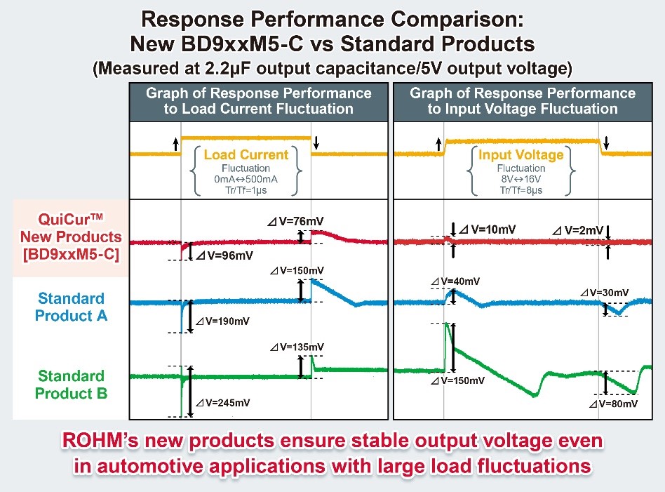
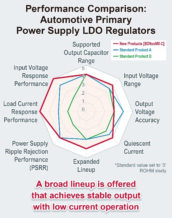
ROHM Develops Automotive Primary LDOs: Leveraging Original QuiCur Technology to Achieve Industry-Leading Load Response Characteristics
Ensures stable output in automotive applications with high input voltage and significant load jumps
ROHM has developed 45V rated 500mA output primary LDO regulators: BD9xxM5-C (BD933M5EFJ-C / BD950M5EFJ-C / BD900M5EFJ-C / BD933M5WEFJ-C / BD950M5WEFJ-C / BD900M5WEFJ-C). These devices are suitable for supplying power to automotive electronic components such as ECUs that operate from vehicle batteries.
In recent years, the number of onboard power supply systems and functions continues to grow as electrification in the automotive industry progresses. This increases the demand for primary LDOs that can directly step down the battery voltage to MCUs and other components used in ECUs. However, the energy supplied by the vehicle’s lead-acid battery is often subject to sudden voltage fluctuations, which primary LDOs are required to provide with excellent line-transient response in these conditions.
At the same time, ECUs and other downstream devices often experience load current variations during operation, which also demand excellent load-transient response characteristics. A high-frequency response is essential for fast output voltage recovery, but it has been difficult to provide sufficient phase margin at the same time to ensure stable operation. In response, ROHM developed a novel solution that addresses these challenges.
The BD9xxM5-C incorporates original QuiCur high-speed load response technology that delivers excellent response characteristics to load current fluctuations. For example, the LDO can maintain output to within 100mV of the set voltage even as the load changes between 0 and 500mA in 1μs (Rise time/Fall time). Furthermore, low 9.5µA (typ.) current consumption contributes to lower power consumption in automotive applications. These new products will be available in four packages, ranging from the compact HTSOP-J8 to the high heat dissipation TO252 (TO252-3/TO252-5) and HRP5 types. This allows users to select the most suitable package for each use case.
Going forward, ROHM will continue to improve reliability while reducing power consumption in automotive applications by developing products utilizing its strengths in analogue and other technologies.
Product Lineup
The new BD9xxM5-C meets the basic requirements for automotive products, including 150°C operation and qualification under the AEC-Q100 automotive reliability standard. A wide range of packages will be available to select from depending on the application environment, all featuring excellent response performance and low current consumption using proprietary QuiCur technology.
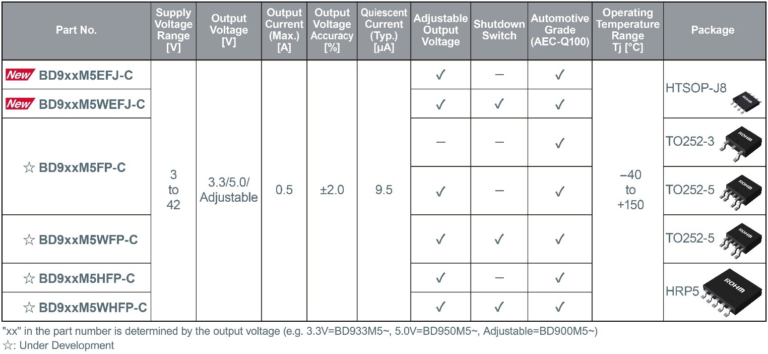
The lineup will be expanded to comprise a total of 18 models, (including the TO252-3, TO252-5, and HRP5 packages) by FY2024.
Application Examples
Suitable for a wide range of automotive applications such as ECUs that operate on vehicle primary power supply systems.
- Powertrain: Fuel Injection (FI), Tire Pressure Monitoring System (TPMS)
- Body Systems: Body Control Modules
- Infotainment: Instrument Clusters, Head-Up Displays (HUDs)
QuiCur High-Speed Load Response Technology
QuiCur is the name of ROHM’s proprietary ‘Quick Current’ high-speed load response circuit capable of maximizing load response characteristics (response performance) without causing instability in the feedback circuits of power supply ICs.
Stable operation of the power supply IC is also possible with minimal output capacitance. And in the case of switching regulators, which are a type of power supply IC, it is possible to linearly adjust the capacitance and output voltage fluctuation to easily achieve stable operation even when the capacitance is changed due to specification changes, significantly reducing the number of person-hours required for power circuit design – both in terms of decreasing component count and ensuring stable operation.
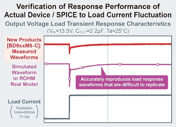
Support Tools
ROHM Real Models are high-accuracy SPICE models that utilize original model-based technology to faithfully reproduce the electrical and temperature characteristics of the actual IC, resulting in a perfect match between the IC and simulation values. This ensures reliable verification, contributing to more efficient application development – for example by preventing rework after prototyping.
Terminology
Primary
In a power supply circuit, the side in charge of 1st stage conversion from a power source such as a battery is called the primary and the side responsible for 2nd stage conversion is referred to as the secondary.
LDO Regulator (Low Drop Out/Low Saturation Regulator)
A type of power supply IC that converts between two different DC voltage levels. Falls under the category of linear regulator (where the input/output voltages operate linearly) characterized by a small input-output voltage difference. Compared to DC-DC converter ICs (switching regulators), LDOs feature a simpler circuit configuration and lower noise.
Load Current
From the point of view of the power supply ICs, all electronic circuits in the subsequent stages, including MCUs and sensors, can be considered “loads”. When these loads operate, a (load) current flows, causing the output voltage of the power supply IC to undershoot (drop) or overshoot. Load transient response characteristics refer to the response time until the changed voltage due to the load current is restored and the power supply stabilizes.
The post ROHM Develops Automotive Primary LDOs: Leveraging Original QuiCur Technology to Achieve Industry-Leading Load Response Characteristics appeared first on ELE Times.
Sky One Emerges as the Leader in Serving the Global Aviation Industry
Sky One is a multinational conglomerate with a strong impact on all areas of aviation. They have ventured into diverse products and services like- Cargo Charter, Asset Trading, MRO, ACMI, Capacity Optimization, Consultancy, Passenger Airlines, Helicopters, Spare parts, Flight Operations Support, Relief Support, and Venture Capital.
Sky One Group has a portfolio of diverse aviation assets both rotor and fixed wing. It operates Bell412, Mi172 helicopters in India and Indonesia, and Boeing 747 and IL76 in the Middle East, Europe, and China, and Bombardier aircraft in India. It also operates a fleet of Mi-8 helicopters. Sky One has a specialized charter business for passengers going for Hajj and Umrah. It specializes in wet leasing with several leading passengers and global cargo airlines from China, Africa, and the Middle East, making it one of the leading privately-owned aviation companies in the Gulf.
 Jaideep Mirchandani, Group Chairman of Sky One FZE
Rashi Bajpai, Sub-Editor at ELE Times had an opportunity to interact with Mr. Jaideep Mirchandani, Group Chairman of Sky One FZE, and discuss various aspects of the global aviation industry and Sky One’s product portfolio and competitive edge.
This is an excerpt from the interview.
ELE Times: How is the aviation sector currently positioned for Sustainable Aviation Fuel (SAF)?
Mr Jaideep: Sustainable Aviation Fuels (SAF) made from biomass or waste-based organic feedstock aim to decrease greenhouse gas emissions in the aviation industry. However, as cited by the World Economic Forum in its 2023 report on SAF (What is SAF and why are only 0.1% of flights powered by it?) there is a need to overcome some key challenges including the substantial cost burden of SAF compared to petroleum jet fuel, the low percentage of global consumption, the necessity for a greater diversity of feedstocks and production methods, and the requirement for a favourable tax policy to incentivize its production.
Many countries are developing strategies for the adoption of SAF. For instance, in January, India’s Civil Aviation Ministry proposed a 1-5% usage of SAF starting in 2027 in alignment with the second phase of the Carbon Offsetting and Reduction Scheme for International Aviation (CORSIA), as suggested by ICAO. Similarly, other major countries have also established SAF volume targets and adoption timelines based on their net zero goals.
Currently, SAF needs to be blended with traditional aviation fuel. Ongoing research aims to use SAF as a direct replacement, eliminating the need for aircraft engine modifications, though this process will take more time.
ELE Times: Tell us about some of the latest technologies and trends that airlines including Sky One are now focusing on to enhance the customer experience.
Mr Jaideep: Today’s passengers seek more than just connectivity; they desire an experience tailored to their individual preferences, right from the moment they book a flight to the time they land. Recognizing the digital sophistication of the new-age passenger, airlines are investing in technology-focused training initiatives to elevate the proficiency of their staff.
This strategic upskilling empowers the workforce to navigate digital platforms and communication tools effectively, ensuring a seamless and user-friendly experience for passengers. At Sky One, our emphasis is also on streamlining operations with a more agile and responsive approach to handling disruptions. We are also leveraging the most efficient communication channels for personalised interactions. I foresee an even more advanced integration of AI not only for customer service but also for predictive maintenance, fuel optimisation, crew scheduling, and revenue management. However, as technology advances, it also brings about potential security and privacy risks, and it is important to effectively manage passengers’ data and ensure their privacy.
ELE Times: What are your views on emerging solutions in “all-electric air mobility service”?
Mr Jaideep: Current reports indicate that many companies are actively developing air taxis and flying cars, with expectations that OEMs will certify them by 2025. Airbus has already announced CityAirbus NextGen, an all-electric, four-seat vertical take-off and landing (eVTOL) prototype based on a lift and cruise concept, featuring an 80-km operational range and a cruise speed of 120 km/h suitable for various flight operations in cities and communities.
In India, the prospects for electric air taxis are bright, as InterGlobe Enterprise, the parent company of IndiGo, has announced plans to launch an all-electric taxi service in 2026 in partnership with the US-based Archer Aviation. Predictions suggest that electric aircraft, capable of taking off like helicopters and flying like airplanes, may enter commercial service by the end of the coming year or early 2026.
As far as my views are concerned, I believe such innovations in aviation are inevitable. However, the air taxi industry may not experience a significant boom until the end of this decade. Initial instances of eVTOL craft are also most likely to be limited to military and cargo applications. Passenger services, I believe, will not only need additional infrastructure facilities but also supportive policy decisions regarding practical applications in urban areas.
ELE Times: Give us a brief overview of your product catalogue, its specifications, and major USP.
Mr Jaideep: Our catalogue includes a wide range of services, such as cargo charters, MRO, wet leasing support to passenger airlines, training, helicopter services, and flight operations support for relief missions. Recently, we’ve inked pacts with Fly Oya from Libya, Uplift Airport Services in Romania, and Cerium Air in Kazakhstan, further expanding our services globally. For startup airlines, we also provide advantageous lease terms on our top-quality aircraft. Further, Pier Seven Aviation, an important part of Sky One, has been committed to delivering high-quality flight training and education to aspiring pilots worldwide since 2015.
At the core of Sky One’s aviation philosophy is humanism, which spurs us to serve, help, and connect individuals and communities in need. This ethos is reflected in our comprehensive services, particularly our active involvement in relief support. We have a dedicated team trained to mobilise swiftly, ensuring the prompt deployment of essential resources, including aircraft, personnel, and equipment, to affected areas dealing with a humanitarian crisis or a natural disaster.
ELE Times: What, in your opinion, are the key growth drivers behind markets like India, and could you provide insights into the market outlook for 2024, with a focus on your expectations?
Mr Jaideep: The International Air Transport Association (IATA) has recently strengthened profitability projections for airlines in 2024, anticipating a notable upswing in the industry’s net overall revenues. The forecast indicates that travel figures will surge to 4.7 billion people in 2024, surpassing pre-pandemic levels—a highly positive sign for the aviation sector. This growth is primarily attributed to emerging economies, with India being highlighted by IATA as one of the most promising markets for global aviation and a key player in shaping the industry’s future landscape.
India’s surge in aviation is fueled by the rapid growth of its domestic sector. According to data compiled by aviation analytics firm Network Thoughts, India’s domestic air travel achieved a historic milestone in 2023, with a record-breaking 15.2 crore passengers—surpassing the previous peak of 14.4 crore passengers in 2019. With the significant emphasis the government is placing on Regional Connectivity Schemes, coupled with a focus on enhanced airport capacity and the addition of new destinations, this will further contribute to maintaining the growth momentum. Domestic travellers can expect an enhanced travel experience in the coming years with more travel options to Tier-II and III cities.
Meanwhile, the international travel trends from India suggest that the Middle East and North America will continue to be major revenue drivers, as has been the case for several years. It is anticipated that the Middle East will persist in dominating the traffic flows from India, with over 40% of international traffic heading to the region, and Dubai alone capturing nearly 15% of it.
The post Sky One Emerges as the Leader in Serving the Global Aviation Industry appeared first on ELE Times.
Indium Corporation Celebrates 90 Years of Materials Science Innovation
Indium Corporation, a global leader in materials science and electronics assembly solutions, commemorated its 90th anniversary on March 13, 2024. Indium Corporation’s innovative products, especially its advanced soldering solutions, are found in many common consumer electronics and high-reliability technologies such as electric vehicles, mobile devices, life-saving medical devices, and emerging 5G technology to name just a few.
Indium Corporation was founded in Utica, NY, U.S. in 1934 by Dr. William S. Murray who was instrumental in identifying and enabling the first commercially viable applications for indium metal. Today, the company is a premier materials refiner, smelter, manufacturer, and supplier to the global electronics, semiconductor, thin-film, and thermal management markets with facilities in China, Germany, India, Malaysia, Singapore, South Korea, the United Kingdom, and the U.S.
The company’s products include solders and fluxes; brazes; thermal interface materials; sputtering targets; indium, gallium, germanium, and tin metals and inorganic compounds; and NanoFoil. Currently, over 5 million EVs are on the road with Indium Corporation’s proven solder and thermal management solutions for high reliability. Additionally, products such as award-winning Durafuse LT and the company’s Reclaim and Recycle initiative are at the forefront of sustainability within the industry.
“This milestone is a testament to the hard work and dedication of our employees, the trust of our customers, and the support of our global partners,” said President and COO Ross Berntson. “It also provides a great opportunity to reflect on our achievements, celebrate our present successes, and envision a richer future enabled by Indium Corporation’s materials science.”
“True to Dr. Murray’s enduring legacy, we continue to be motivated by curiosity to view materials in new ways,” Berntson added. “Fueled by a commitment to research and development, our industry thought leaders and cutting-edge products, Indium Corporation continues to innovate and grow.”
Indium Corporation is committed to playing a leadership role in the future of the global electronics assembly industry. In 2023 alone, the company joined the American Semiconductor Innovation Coalition (ASIC), European Center for Power Electronics (ECPE), and India Electronics and Semiconductor Association (IESA). Within the same year, Indium Corporation was also honoured with CIRCUITS ASSEMBLY’s New Product Introduction Award, EM World’s Innovation Award, IEEE Malaysia’s Outstanding Industry Award for Innovation, Electronics Maker’s Best of Industry Award for Best Soldering Product of the Year, two Global Technology Awards from Global SMT & Packaging in Flux and Adhesive/Underfills/Encapsulants categories, Mexico EMS’ Mexico Technology Award for Solder Paste, and SMTA’s Technical Distinction Award bestowed upon Dr. HongWen Zhang.
In addition to its industry-leading products and technical expertise, Indium Corporation also proudly supports the communities in which it operates through charitable contributions, advancing STEM education at all levels, and fostering workforce development in STEM industries. Indium Corporation also works with military veterans to make successful transitions to private sector careers. Through its outreach efforts, the company impacts more than 5,000 lives annually.
“Just as we believe that materials science changes the world, we believe that today’s students will build our future successes,” said Associate Vice President of Human Resources Dawn Roller. “To that end, we are committed to bolstering community educational resources, especially those that advance the promise and vitally important work being done in STEM fields.”
The post Indium Corporation Celebrates 90 Years of Materials Science Innovation appeared first on ELE Times.
Pages

