
ELE Times

Emerging solutions in all-electric air mobility service
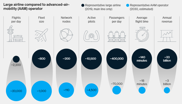
With projections indicating a doubling of air passenger numbers to 8.2 million by 2037, the advancement of all-electric and hybrid-electric propulsion for powering Advanced Air Mobility (AAM) is evolving into a billion-dollar industry. Recent assessments by Rolls Royce suggest that approximately 15,000 Electric Vertical Take-Off and Landing (eVTOL) vehicles will be indispensable across 30 major cities by 2035 solely to meet the demand for intracity travel. By 2030, top players in the passenger Advanced Air Mobility (AAM) sector could boast larger fleets and significantly more daily flights than the world’s biggest airlines. These flights, averaging just 18 minutes each, will typically carry fewer passengers (ranging from one to six, plus a pilot).
The increasing urbanization, expanding population, aging infrastructure, and the surge in e-commerce and logistics underscore the need for a contemporary, safe, and cost-effective transportation solution for both people and goods. Urban Air Mobility (UAM) presents a seamless, reliable, and swift mode of transportation, addressing present and future urban challenges. With the capacity to transform intra and inter-city transportation, UAM offers a quicker and more effective alternative to conventional ground-based transportation methods. The adoption of Urban Air Mobility hinges on five primary factors:
- Growing demand for alternate modes of transportation in urban mobility.
- Need for convenient, efficient and last mile delivery.
- Zero emission and noise free mandates.
- Advancement in technologies (Energy storage, Autonomous, Connected, Power Electronics).
- Security.
Despite the growing Urban Air Mobility (UAM) sector, it faces significant challenges that need addressing for future growth and success. These challenges range from developing reliable electric propulsion systems to achieving autonomous flight capabilities and establishing necessary infrastructure like vertiports and charging stations. Overcoming these hurdles is vital for unlocking UAM’s transformative potential in urban transportation.
AI Integration for UAM EnhancementUtilizing AI for predictive maintenance enables analysis of sensor data and onboard sources to forecast maintenance needs, reducing downtime and increasing aircraft availability. AI-enabled maintenance inspections allow for rapid issue identification through image analysis of eVTOLs and UAVs, minimizing errors and oversights. AI aids in making better decisions for aircraft maintenance support by thoroughly analyzing various considerations, likely leading to improved outcomes. Additionally, robotic systems equipped with AI algorithms can autonomously repair or replace minor parts, enhancing safety for maintenance teams. Moreover, AI facilitates better diagnostics and targeted troubleshooting, expediting issue identification and repair suggestions. Ultimately, proactive maintenance, data integration, and improved safety are promised by AI in UAM, ensuring aircraft are maintained effectively from takeoff to landing.
AI in Intelligent Cabin Management (ICMS)The Intelligent Cabin Management System (ICMS), utilized in aviation and rail industries, undergoes continuous advancements fueled by emerging technologies. Enhanced facial recognition algorithms, driven by artificial intelligence (AI), significantly improve efficiencies and reliability in user authentication, behavior analysis, safety, threat detection, and object tracking. Moreover, ICMS prioritizes monitoring passengers’ vital signs onboard for health safety.
This solution ensures cabin operations with a focus on passenger safety, security, and health, suitable for various passenger cabins in aircraft and rail, and particularly ideal for UAM applications. It facilitates cabin entry by authorized crew and passengers, guides seating arrangements, enforces luggage placement regulations, ensures compliance with air travel advisories, monitors passenger behavior for preemptive intervention, identifies permitted and potentially threatening objects, flags left luggage, and detects vital health parameters for real-time monitoring and control.
AI in UAM MaintenanceAI-driven predictive maintenance involves analyzing sensor data and onboard sources to anticipate UAM maintenance needs, aiding in proactive scheduling and minimizing downtime. Similarly, AI-based inspections utilize image analysis to swiftly identify potential issues during regular checks, enhancing accuracy and reducing errors. Additionally, AI supports maintenance decision-making by analyzing various factors like repair costs and part availability, providing informed recommendations. Future advancements may see autonomous maintenance systems, powered by AI, performing routine tasks such as inspections and minor repairs, improving efficiency and safety. Furthermore, AI assists technicians in diagnostics and troubleshooting by analyzing data and historical records to pinpoint issues and suggest appropriate solutions, streamlining maintenance processes and ensuring UAM operational reliability.
ConclusionThe integration of AI into UAM maintenance offers numerous benefits that significantly enhance the efficiency, safety, and reliability of UAM operations. Through proactive maintenance enabled by AI’s predictive capabilities, maintenance teams can anticipate and address potential failures before they occur, reducing unplanned downtime and enhancing operational reliability. Furthermore, AI-supported maintenance increases aircraft availability, ensuring vehicles are consistently safe and reliable, thus contributing to higher customer satisfaction and overall operational performance.
Moreover, AI-driven maintenance optimization leads to cost reduction by accurately predicting maintenance needs and minimizing unnecessary inspections and component replacements, thereby reducing labor and material costs. Additionally, AI’s continuous monitoring of UAM vehicle conditions enhances safety by detecting anomalies or safety risks in real-time, preventing accidents and ensuring timely maintenance. Overall, the application of AI in UAM maintenance represents a transformative step towards a more efficient, safe, and reliable urban air transportation system.
 Ajay Kumar Lohany | Delivery Sr. Director- Aero & Rail | Cyient
The post Emerging solutions in all-electric air mobility service appeared first on ELE Times.
Automotive PCIe: To Switch or Not to Switch?
Courtesy : Microchip
The myths and false economy of direct chip-to-chip PCIe connect in ADAS and vehicle autonomy applications.
PCIe’s Rising Role in Autonomous Driving and ADAS TechnologyBefore pondering the question of whether or not to switch, let’s first set the scene by considering why Peripheral Component Interconnect Express (PCIe) is becoming so popular as an interconnect technology in advanced driver assistance systems (ADAS) applications—and why it will be so crucial in the realization of completely autonomous driving (AD) as the automotive industry seeks standard interfaces that deliver performance while ensuring compatibility and ease-of-use.
With its roots in the computing industry, PCIe is a point-to-point bidirectional bus for connecting high-speed components. Subject to the system architecture (PCIe’s implementation), data transfer can take place over 1, 2, 4, 8 or 16 lanes, and if more than one lane is used the bus becomes a serial/parallel hybrid.
The PCIe specification is owned and managed by the PCI Special Interest Group (PCI-SIG), an association of 900+ industry companies committed to advancing its non-proprietary peripheral technology. As demand for higher I/O performance grows, the group’s scope and ecosystem reach are both expanding, and to paraphrase words from PCI-SIG’s membership page:
Current PCIe and other related technology roadmaps account for new form factors and lower power applications. Innovation on these fronts will remain true to PCI-SIG’s legacy of delivering solutions that are backward compatible, cost-efficient, high performance, processor agnostic, and scalable.
With vehicles becoming high-performance computing platforms (HPCs—and data centers, even) on wheels, these words are exactly what vehicle OEMs developing ADAS and AD solutions want to hear. Also, every generation of PCIe results in performance improvements – from gen 1.0’s data (giga) transfer rate of 2.5GT/s and total bandwidth of 4G/s (16 lanes) to today’s gen 6.0’s 64GT/s and 128G/s (16 lanes). Note: PCIe 7.0, slated to arrive in 2025, will have a data rate of 128GT/s and a bandwidth of 512GB/s through 16 lanes.
PCIe’s performance power cannot be disputed, and it will certainly be required to support the kind of real-time processing of large volumes of data needed for AI- and ML-enabled ADAS and AD applications.
But, as ever, there is debate around implementing PCIe-based architectures, not least when it comes to whether the connections between PCIe-enabled components should be direct or switched.
Making the ConnectionTo provide higher levels of automation, vehicles must incorporate increasingly sophisticated combinations of electronic components including central processing units (CPUs), electronic control units (ECUs), graphics processing units (GPUs), system-on-chips (SoCs), “smart sensors” and high-capacity and high-speed storage devices (such as NVMe memory).
Of these components, the ECUs (there are many) combine across separate zones based on a common functionality. These zonal ECUs communicate with HPC platforms using Ethernet. But within those platforms, there is a need for high-bandwidth processing to achieve real-time decision making.
Accordingly, PCIe technology is being used by automotive designers in a manner very similar to the way in which a data center is designed. Connecting sensors with high-speed serial outputs to processing units is best addressed with an open standard called Automotive SerDes Alliance (ASA).
In essence, there are three pillars of automotive networking (see figure 1).
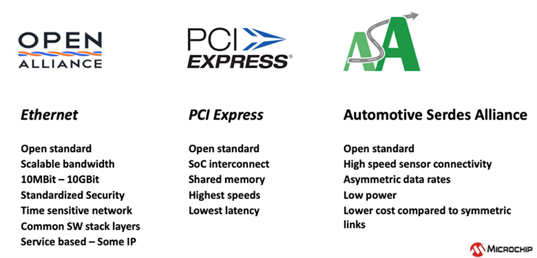 Figure 1 – Three Pillars of future of Automotive Networking
However, some SoC vendors are saying that for PCIe you can simply connect directly between chips without a switch. Well, yes, you can… but it doesn’t scale to higher ADAS levels and it’s a false economy do so.
An HPC system without a switch exponentially increases software complexity, as each end requires its own software stack. Also, there’s the “bigger picture” benefits of switched over unswitched PCIe to consider:
- IO Bandwidth Optimization: Packet switching reduces the SoC interconnection pin count requirement which lowers SoC power and cost.
- Peripheral Sharing: Single peripherals, such as SSD storage or ethernet controllers, may be shared across several SoCs
- Scalability: You can easily scale for more performance without changing the system architecture by increasing switch size, SoC count and peripheral count.
- Serviceability: PCIe has built-in error detection and diagnostic test features which have been thoroughly proven in the high-performance compute environment over many years to significantly ease serviceability.
- And as a result of the above points, a much better total cost of ownership (TCO) is possible.
When PCIe combines forces with Ethernet and ASA, it allows for the creation of an optimized, heterogeneous system architecture (as figure 2 illustrates with respect to an ADAS example).
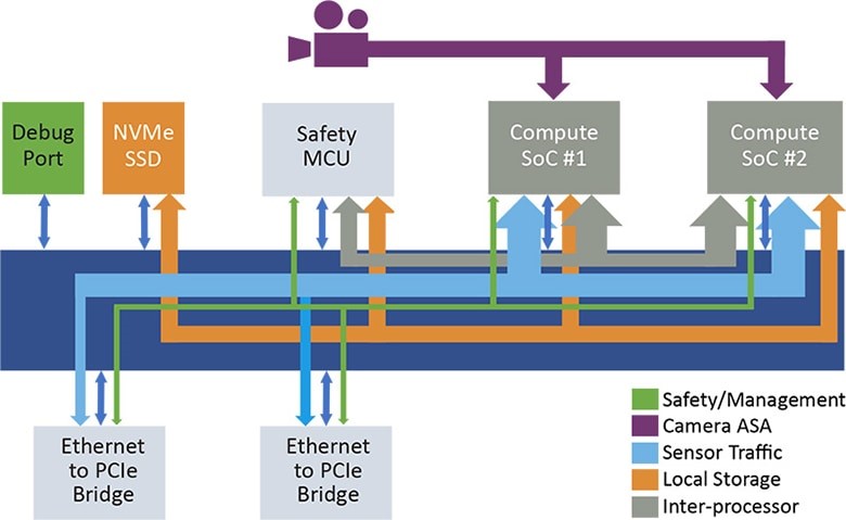 Figure 2 – Heterogenous architecture for ADAS
Although the three communications technologies evolved at different times to support different needs, and have their respective pros and cons, the heterogeneous architecture makes the best of each.
As mentioned, PCIe provides point-to-point connection, meaning devices are not competing for bandwidth, which is fine if only a few devices need to connect. However, an autonomous vehicle is best realized as a set of distributed workloads, which means bandwidth needs to be shared between multiple sub-system components.
In this respect, PCIe switches provide an excellent solution as they are “transparent,” meaning that software and other devices do not need to be aware of the presence of switches in the hierarchy, and no drivers are required.
The Answer: SwitchPCIe is ideal for ADAS, AD and other HPC applications within a vehicle, but its “point-to-point” connectivity has many thinking that that’s how it should be implemented—as chip-to-chip, for example. However, integrating switching using technologies such as the Microchip Switchtec family (the world’s first automotive-qualified PCIe switches) minimizes software complexity and realizes a host of other benefits for high-performance automotive systems with multiple sub-system components that demand low latencies and high data rates.
The post Automotive PCIe: To Switch or Not to Switch? appeared first on ELE Times.
Techniques to Identify and Correct Asymmetric Wafer Map Defects Caused by Design and Process Errors
JAMES KIM, Senior Semiconductor and Process Integration Engineer | Lam Research
Asymmetries in wafer map defects are usually treated as random production hardware defects. For example, asymmetric wafer defects can be caused by particles inadvertently deposited on a wafer during any number of process steps. In this article, I want to share a different mechanism that can cause wafer defects. Namely, that these defects can be structural defects that are caused by a biased deposition or etch process.
It can be difficult for a process engineer to determine the cause of downstream structural defects located at a specific wafer radius, particularly if these defects are located in varying directions or at different locations on the wafer. As a wafer structure is formed, process behavior at that location may vary from other wafer locations based upon the radial direction and specific wafer location. Slight differences in processes at different wafer locations can be exaggerated by the accumulation of other process steps as you move toward that location. In addition, process performance differences (such as variation in equipment performance) can also cause on-wafer structural variability.
In this study, structural defects will be virtually introduced on a wafer to provide an example of how structural defects can be created by differences in wafer location. We will then use our virtual process model to identify an example of a mechanism that can cause these types of asymmetric wafer map defects.
Methods Figure 1. Anisotropic liner/barrier metal
deposition on a tilted structure caused by wafer warping
A 3D process model of a specific metal stack (Cu/TaN/Ta) on a warped wafer was created using SEMulator3D virtual fabrication (Figure 1). After the 3D model was generated, electrical analysis of 49 sites on the wafer was completed.
In our model, an anisotropic barrier/liner (TaN/Ta) deposition process was used. Due to wafer tilting, there were TaN/Ta deposition differences seen across the simulated high aspect ratio metal stack. To minimize the number of variables in the model, Cu deposition was assumed to fill in an ideal manner (without voids). Forty-nine (49) corresponding 3D models were created at different locations on the wafer, to reflect differences in tilting due to wafer warping. Next, electrical simulation was completed on these 3D models to monitor metal line resistance at each location. Serpentine metal line patterns were built into the model, to help simulate the projected electrical performance on the warped wafer at different points on the same radius, and across different directions on the wafer (Figure 2).
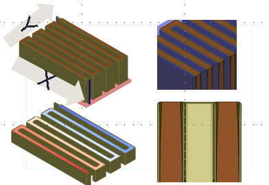 Figure 2 – Techniques to Identify and Correct Asymmetric Wafer Map Defects Caused by Design and Process Errors
Using only incoming structure and process behavior, we can develop a behavioral process model and extend our device performance predictions and behavioral trend analysis outside of our proposed process window range. In the case of complicated processes with more than one mechanism or behavior, we can split processes into several steps and develop models for each individual process step. There will be phenomena or behavior in manufacturing that can’t be fully captured by this type of process modeling, but these models provide useful insight during process window development.
ResultsOf the 49 3D models, the models on the far edge of the wafer were heavily tilted by wafer warpage. Interestingly, not all of the models at the same wafer radius exhibited the same behavior. This was due to the metal pattern design. With anisotropic deposition into high aspect ratio trenches, deposition in specific directions was blocked at certain locations in the trenches (depending upon trench depth and tilt angle). This affected both the device structure and electrical behavior at different locations on the wafer.
Since the metal lines were extending across the x-axis, there were minimal differences seen when tilting the wafer across the x-axis in our model. X-axis tilting created only a small difference in thickness of the Ta/TaN relative to the Cu. However, when the wafer was tilted in the y-axis using our model, the high aspect ratio wall blocked Ta/TaN deposition due to the deposition angle. This lowered the volume of Ta/TaN deposition relative to Cu, which decreased the metal resistance and placed the resistance outside of our design specification.
X-axis wafer tilting had little influence on the device structure. The resistance on the far edge of the x-axis did not significantly change and remained in-spec. Y-axis wafer tilting had a more significant influence on the device structure. The resistance on the far edge of the y-axis was outside of our electrical specification (Figure 3).
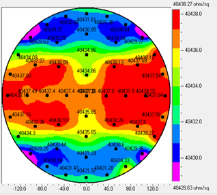 Figure 3 – Techniques to Identify and Correct Asymmetric Wafer Map Defects Caused by Design and Process Errors
Conclusion
Figure 3 – Techniques to Identify and Correct Asymmetric Wafer Map Defects Caused by Design and Process Errors
Conclusion
Even though wafer warpage occurs in a circular manner due to accumulated stress, unexpected structural failures can occur in different radial directions on the wafer due to variations in pattern design and process behavior across the wafer. From this study, we demonstrated that asymmetric structures caused by wafer warping can create top-bottom or left-right wafer performance differences, even though processes have been uniformly applied in a circular distribution across the wafer.
Process simulation can be used to better understand structural failures that can cause performance variability at different wafer locations. A better understanding of these structural failure mechanisms can help engineers improve overall wafer yield by taking corrective action (such as performing line scanning at specific wafer locations) or by adjusting specific process windows to minimize asymmetric wafer defects.
The post Techniques to Identify and Correct Asymmetric Wafer Map Defects Caused by Design and Process Errors appeared first on ELE Times.
Executive Blog – Companies that Embrace Digital Transformation Have More Resilient Design and Supply Chains
Sailesh Chittipeddi | Executive Vice President Operations | Renesas
Digital transformation has evolved quickly from a conceptual phase to a semiconductor industry change agent. The rapid take up of AI-enhanced product development is only accelerating this transformation and is further influenced by two connected trends: The movement of Moore’s Law from transistor scaling to system-level scaling, and the relatively recent redistribution of the global electronics supply chain due to the COVID-19 pandemic.
I spoke on this subject earlier this month at the Industry Strategy Symposium 2024 in Half Moon Bay, California, where leaders from across the chip industry gather annually to share their insights on technology and trend drivers and what they could mean for our respective businesses.
Between the early 1970s and around 2005, increased chip performance was largely a function of clock frequency improvements driven by advances in lithography, transistor density, and energy efficiency. With increasing transistor counts (and die size), clock frequencies are limited by interconnect delays and not by transistor performance. To overcome this challenge, designers moved to multi-core designs to increase system performance without blowing up energy. Novel packaging techniques such as chiplets and multi-chip modules are helping further improve system performance, particularly in AI chips.
A single chip package may be comprised of multiple chiplets each housing specific functions such as high-performance logic elements, AI accelerators, high-bandwidth DDR memory, and high-speed peripherals. Very often, each of these components is sourced from a different fab, a trend that has resulted in a fragmented global supply chain. This creates its own set of challenges as die from multiple fabs must be integrated into a package or system that must then be thoroughly tested. Test failures at this stage have enormous financial consequences. These challenges, require a “shift left” mindset in product development. The shift left mentality has major ramifications for how we, as an industry, should be managing our supply chains by moving the heavy emphasis from architecture/design to final system testing and quality.
Supply chain challenges during the COVID pandemic have resulted in further decentralization of the supply chain components. To illustrate the enormity of the change underway, consider that between 2022 and December 2024 construction began on 93 wafer fabs around the world. Compare that to the global construction of automated test facilities. In 2021 alone, the industry broke ground on 484 back-end test sites, which provides a measure of how committed the chip sector is to driving resiliency across the manufacturing landscape.
The Role of AI in Semiconductor Design and ManufactureSo, where does AI come into the picture?
A key area in which AI will exert its influence is the shift from an analytic to a predictive model. Today, we wait to detect a problem and then look at past data to identify the root cause of the problem and prevent it from reoccurring. This inefficient approach adds time, cost, unpredictability, and waste to the supply chain. AI, on the other hand, allows us to examine current data to predict future outcomes.
Instead of using spreadsheets to analyze old data, we build AI models that production engineers continuously train with new data. This “new” data is no longer merely a set of numbers or measurements but includes unstructured data such as die photos, equipment noise, time series sensor data, and videos to make better predictions.
In the end, it’s about pulling actionable information from a sea of data points. In other words, data without action is mostly useless. Why am I driving this point home? Because today, 90 percent of data created by enterprises is never used. It’s dark data. And when you think about AI implementation, 46 percent of them never make it from pilot to production because the complexity of the programs is not scoped appropriately.
Despite these challenges, equipment makers are already starting to implement digital transformation techniques into their product development processes. The benefits are palpable. Research from Boston Consulting Group found that companies that have built resiliency into their supply and design chains recovered from COVID-related downturns twice as fast as companies that have yet to embrace digital transformation.
At Renesas, we acquired a company called Reality AI that generates a compact machine learning model that runs on a microcontroller or microprocessor. This provides the unique ability to quickly detect deviations from normal patterns that may cause equipment problems. It allows manufacturing facilities to schedule preventive maintenance or minimize downtime associated with sudden equipment failure.
Digital Transformation Is Future-Proofing Our IndustryDigital transformation with AI is key to business success today. As the semiconductor industry undergoes a major evolution – embracing system-level design and adapting to a changing global supply chain – digital transformation and the shift left approach are powerful tools that deliver on two fronts.
The first is a productivity increase that comes from optimized tools and design processes. The closer you are to where the failure is likely to occur, the more quickly you learn and the more quickly you can fix things.
Second, and perhaps most importantly, digital transformation solves one of the biggest problems the industry has with chip design – the availability of talent. When we reduce the time taken to design a chip, we’re making our engineers far more efficient than they would be otherwise, which is increasingly important as the semiconductor industry demographic skews older.
The post Executive Blog – Companies that Embrace Digital Transformation Have More Resilient Design and Supply Chains appeared first on ELE Times.
Network RTK vs PPP-RTK: an insight into real-world performance
By- Patty Felts, Product Marketing Manager, Product Center Services
Australian automation and positioning technology provider conduct static and kinematic tests
Locating people, animals, or objects on Earth with high precision requires the use of GNSS receivers and the support of network RTK correction services that account for errors caused by the atmosphere, satellite clock drift, and signal delays.
Three standard approaches to correct these errors are Real Time Kinematic (RTK), Precise Point Positioning (PPP) GNSS correction services, and a combination of the two, PPP-RTK. Beyond these, a pairing device such as a survey-grade GNSS receiver or a mass-market smart antenna is also required to enhance positioning accuracy. Combining any of these approaches with one device will optimize the positioning accuracy of the end-use application.
Many GNSS navigation applications require high accuracy. The accuracy of survey-grade GNSS receivers exceeds what mass-market smart antennas can provide. Of course, this comes at a price. Still, several high-precision GNSS navigation applications can do well with the accuracy offered by mass-market smart antennas. Examples include transportation, e-mobility, IoT use cases, and field robotics. Designers aim to equip devices with reliable, high-precision positioning at a reasonable cost.
GNSS users can verify the capabilities of setups by hitting the roads and testing them in real-world situations. Doing so enables them to understand the capabilities of these setups and differentiate them.
Aptella (formerly branded as Position Partners), an Australasian provider of automation and positioning technology solutions, had the opportunity to test the capabilities of network RTK vs PPP-RTK GNSS correction services and present the findings to their client.
We will discuss the findings, but as a first step, let us review how the RTK, PPP, and PPP-RTK approaches operate, the equipment needed, and the participants in this exercise.
Network RTK, Precise Point Positioning GNSS, and PPP-RTKThe mentioned correction approaches follow different paths. RTK GNSS correction services calculate and correct GNSS errors by comparing satellite signals from one or more reference stations. Any errors detected are then transmitted using IP-based communications, which can be reliable beyond a radius of 30 km from the nearest base station. Network RTK typically requires bi-directional communication between the GNSS receiver and the service, making the solution more challenging to scale. This approach can provide centimeter-level positioning accuracy in seconds.
Precise Point Positioning GNSS correction services operate differently. They broadcast a GNSS error model valid over large geographic regions. Because this service requires only unidirectional communication (IP-based or via satellite L-band), it’s more scalable to multiple users, unlike RTK.
PPP high-precision positioning takes between three minutes and half an hour to provide a position estimate with an accuracy of less than 10 cm. Static applications such as surveying or mapping typically use this solution, but it can be a poor fit for dynamic applications such as unmanned aerial vehicles or mobile robotics.
More recently, both approaches have been combined into what is known as PPP-RTK GNSS correction services (or State Space Representation (SSR) correction services). This combination provides the accuracy of the RTK network and its fast initialization times with the broadcast nature of Precise Point Positioning. Similar to PPP, the approach is based on a model of GNSS errors that has broad geographic validity. Once a GNSS receiver has access to these PPP-RTK correction data through one-way communication, it computes the GNSS receiver position.
Survey-grade GNSS receiver versus mass-market smart antennaSurvey-grade receivers are devices typically used for geodetic surveying and mapping applications. They are designed to provide highly accurate and precise positioning information for civil engineering, construction, GIS data, land development, mining, and environmental management.
Today’s modules can access data from multiple satellite constellations and network RTK support. These devices are typically very expensive, costing thousands of dollars each, because they are highly precise, with accuracies ranging from centimeters to millimeters.
Mass-market smart antennas are specialized receiver/antenna-integrated devices designed to receive signals from satellite constellations and GNSS correction services right out of the box. Smart antennas capture and process raw data to determine precise locations. Standalone GNSS antennas don’t have a precision rating, as this depends on the integrated GNSS receiver and correction service to which the antennas are coupled.
While mass-market smart antennas are more affordable than survey-grade GNSS receivers, there is a corresponding performance trade-off, with accuracies ranging from a few centimeters to decimeters.
The following tests used a survey-grade GNSS receiver to verify control coordinates in static mode and compare RTK versus PPP-RTK results in the kinematic mode. The GNSS smart antenna was also employed as a pairing device for these static and kinematic tests.
Participating companiesAptella is the company that conducted the performance test and presented the results to their client. However, the participation of four other companies was crucial.
AllDayRTK operates Australia’s highest-density network of Continuously Operating Reference Stations (CORS). Its network RTK correction services were used to compare with PPP-RTK.
u-blox’s PointPerfect provided the PPP-RTK GNSS correction services used in these tests.
Both correction services were coupled with a survey GNSS receiver, Topcon HiPer VR, and a mass-market smart antenna, the Tallysman TW5790.
Testing two correction services solutionsIn the Australian city of Melbourne, Aptella conducted static and kinematic tests with several objectives in mind:
- Test RTK and PPP-RTK GNSS corrections using a mass-market GNSS device like the Tallysman TW5790.
- Demonstrate the capabilities of the Tallysman smart antenna coupled with PPP-RTK corrections.
- Evaluate PointPerfect PPP-RTK GNSS corrections and assess “real world” results against published specifications.
- Determine whether these specifications meet mass-market applications and e-transport safety requirements of 30 cm @ 95%.
- Provide insight into use cases and applications suitable for PPP-RTK corrections.
 Figure 1: gnss antenna and survey grade receiver
These tests allowed experts to compare the accuracy of RTK and PPP-RTK GNSS correction services supported by a mass-market Tallysman smart antenna. They were also able to verify the PPP-RTK performance specifications published by u-blox.
First, a survey-grade Topcon HiPer VR GNSS receiver was used to verify the control coordinates in static mode. Once these were obtained, the Tallysman smart antenna took its place.
The table below summarizes representative results from both methods, PPP-RTK and RTK. Horizontal (planar) accuracy is similar for both, while the vertical accuracy is less accurate with PPP-RTK than RTK.
The horizontal accuracy level of RTK and PPP-RTK is in the centimeter range. In contrast, RTK maintains a centimeter range at the vertical accuracy level, but the PPP-RTK correction errors were in the decimeter range.
| GNSS augmentation
|
Horizontal error (m) | Vertical error (m) | Horizontal 95% (m) | Vertical 95% (m) |
| RTK AllDayRTK | 0.009 | 0.010 | 0.012 | 0.018 |
| PointPerfect PPP-RTK | 0.048 | 0.080 | 0.041 | 0.074 |
Furthermore, the accuracy of the mass market device is within published specifications to meet the 30 cm @ 95% for location (plan) even when obstructed. Still, when measuring heights, these were less accurate than 2D horizontal coordinates. Absolute horizontal location accuracy meets the mass market requirement of 30 cm @ 95%, although RTK is more accurate at a vertical level than PPP-RTK.
Kinematic resultsOn the streets of Melbourne, Aptella experts tested RTK and PPP-RTK corrections operating in different kinematic modes with variable speeds, such as walking under open skies and driving in different environments.
The test setup using an RTK network consisted of AllDayRTK corrections and a survey-grade GNSS receiver. On the other hand, the PPP-RTK test setup was supported by u-blox PointPerfect and the Tallysman smart antenna. The antennas for both setups were mounted on the roof of the vehicle and driven through different routes to encounter various GNSS conditions.
Walking in the open sky: This test involved a walk along the riverbank. Comparing the results, both were similar, proving that PPP-RTK is well-suited for mass-market applications.
 Figure 2: walking tests with rtk and ppp-rtk
On-road driving with varying conditions: This test consisted of driving on Melbourne roads in different conditions, including open skies and partial or total obstructions to GNSS. The route included driving under bridges and areas with multipath effects. Vegetation in the area at the start of the test prevented the smart antenna’s IMU from initializing. No IMU/dead reckoning capability was used during the drive test.
The results obtained while the vehicle moved through a long tunnel under the railroad tracks were of utmost importance. In this situation, the PPP-RTK approach reported a position even in an adverse environment. In addition, PPP-RTK reconverged shortly after RTK.
 Figure 3: rtk vs ppp-rtk under railway bridge in melbourne
Another revealing result of this second test was that the Tallysman smart antenna didn’t seem to deviate from its path when passing under short bridges.
 Figure 4: rtk vs ppp-rtk under a short bridge
Driving through an outage: The outage test took place in an extended, challenging environment for GNSS. This occurred when the car drove under the pedestrian overpass at the Melbourne Cricket Ground. The PPP-RTK solution maintained the travel trajectory and effectively tracked the route (in yellow). On the other hand, the RTK network solution reported positions off the road and on the railway tracks. In this outage condition, RTK took a long time to reconverge to a fixed solution.
 Figure 5: correction services tests under a long structure
Open-sky driving: The final on-road test was conducted in an open-sky environment where the two setups performed similarly. They provided lane-level accuracy and suitability for mass-market applications. However, ground truthing and further testing are required to fully evaluate the accuracy and reliability of PPP-RTK in these conditions.
 Figure 6: correction services comparison driving through Melbourne
Final remarks
Figure 6: correction services comparison driving through Melbourne
Final remarks
The five static and dynamic tests conducted by Aptella were instrumental in assessing the effectiveness of different setups to determine the position of stationary and moving entities.
- From the static test, Aptella concluded that PPP-RTK, coupled with the Tallysman smart antenna, provides centimeter-level horizontal accuracy and performs similarly to RTK. However, this was not the case for vertical accuracy, with PPP-RTK at the decimeter level.
- Regarding the kinematic tests, Aptella obtained significant results, particularly when the environment impeded communication with GNSS. Even without IMU or dead reckoning, the PPP-RTK performed well with lane-level tracking. With short outages such as railway bridges and underpasses, PPP-RTK maintained an acceptable trajectory, while RTK required a long time to reconverge after emerging from these challenging conditions.
- Overall, Aptella has demonstrated that the PPP-RTK and GNSS smart antenna combination delivers results suitable for mass-market applications requiring centimeter-level horizontal accuracy.
As mentioned above, survey-grade devices are costly although highly accurate. A combination of survey-grade GNSS receiver and network RTK correction service is recommended in geodetic surveying use cases that require high height accuracy.
Conversely, mass-market smart antenna devices using PPP-RTK corrections are less expensive but also less accurate. Nevertheless, they are well suited for static applications that don’t require GNSS heights at survey grade.
For many high-precision navigation applications, such as transportation, e-mobility, and mobile robotics, PPP-RTK is sufficient to achieve the level of performance these end applications require. The relative affordability of smart antenna devices, combined with PPP-RTK’s ability to broadcast a single stream of corrections to all endpoints, makes it easier to scale from a few prototypes to large fleets of mobile IoT devices.
The post Network RTK vs PPP-RTK: an insight into real-world performance appeared first on ELE Times.
Unparalleled capacitance for miniaturized designs: Panasonic Industry launches new ZL Series Hybrid capacitors
The compact and AEC-Q200-compliant EEH-ZL Series stands out with industry-leading capacitance and high Ripple Current specs
The ZL series is the latest offspring of Panasonic Industry’s Electrolytic Polymer Hybrid capacitor portfolio. Related to its compact dimensions, it offers unrivalled capacitance values – and hence might evoke a remarkable market echo:
Capacitance: For five case sizes from ø5×5.8 mm to ø10×10.2 mm, the ZL series offers the largest capacitance in the industry and exceeds the values of competitor standard products by approximately 170%.
Ripple Current performance outnumbers the competitor products’ specs besides lower ESR within the same case size.
The new ZL is AEC-Q200 compliant, enforcing strict quality control standards, particularly crucial for the automotive industry. It boasts high-temperature resistance, and is guaranteed to operate at 125°C and 135°C at 4000h. With a focus on durability, the ZL series offers vibration-proof variants capable of withstanding shocks up to 30G, making it a reliable choice.
In summary, this next-generation, RoHS qualified Hybrid Capacitor stands as the ultimate solution for automotive and industrial applications, where compact dimensions are an essential prerequisite.
Tailored for use in various automotive components including water pumps, oil pumps, cooling fans, high-current DC to DC converters, and advanced driver-assistance systems (ADAS), it also proves invaluable in industrial settings such as inverter power supplies for robotics, cooling fans, and solar power systems. Furthermore, it serves a pivotal role in industrial power supplies for both DC and AC circuits, spanning from inverters to rectifiers, and finds essential application in communication infrastructure equipment such as base stations, servers, routers, and switches.
The post Unparalleled capacitance for miniaturized designs: Panasonic Industry launches new ZL Series Hybrid capacitors appeared first on ELE Times.
DDS Option for high-speed AWGs generates up to 20 sine waves
20 independent sine waves up to 400 MHz can be controlled on one generator channel
Spectrum Instrumentation has released a new firmware option for its range of versatile 16-bit Arbitrary Waveform Generators (AWGs) with sampling rates up to 1.25 GS/s and bandwidths up to 400 MHz. The new option allows users to define 23 DDS cores per AWG-card, that can be routed to the hardware output channels. Each DDS core (sine wave) can be programmed for frequency, amplitude, phase, frequency slope and amplitude slope. This enables, for example, the control of lasers through AODs and AOMs, as often used in quantum experiments, with just a few simple commands – instead of making large data array calculations. The DDS output can be synchronized with external trigger events or by a programmable timer with resolution of 6.4 ns.
DDS – Direct Digital Synthesis – is a method for generating arbitrary periodic sine waves from a single, fixed-frequency reference clock. It is a technique widely used in a variety of signal generation applications. The DDS functionality implemented on Spectrum Instrumentation’s AWGs is based on the principle of adding multiple ‘DDS cores’ to generate a multi-carrier (multi-tone) signal with each carrier having its own well-defined frequency, amplitude and phase.
Advantages of using DDS for arbitrary waveform generatorsWith the ability to switch between the normal AWG mode (which generates waveforms out of pre-programmed data) and the DDS mode (which needs only a few commands to generate sine wave carriers), the Spectrum AWGs are highly versatile and can be adapted to almost any application. In DDS-mode, the AWG acts as a base for the multi-tone DDS. The units built-in 4 GByte of memory and fast DMA transfer mode then allows the streaming of DDS commands at a rate as high as 10 million commands per second! This unique capability provides the flexibility to perform user-defined slopes (e.g. s-shaped) as well as various modulation types (e.g. FM and AM) with simple, easy-to-use, DDS commands.
DDS in Quantum Experiments In DDS-mode, only a few commands are needed to e.g. generate a sine wave (orange block), accelerate the frequency (blue block) and lower the amplitude (green block).
For years now, Spectrum AWGs have been successfully used worldwide in pioneering quantum research experiments. Since 2021, Spectrum Instrumentation has been part of the BMBF (German federal ministry of education and research) funding program ‘quantum technologies – from basic research to market’ as part of the Rymax One consortium. The aim of this consortium is building a Quantum Optimizer. The development of the DDS option was based on feedback from the consortium partners and other research institutes worldwide.
The flexibility and fast streaming-mode of Spectrum’s AWGs, which also enables data to be streamed straight from a GPU, allows the control of Qubits directly from a PC. While using an AWG in this way offers full control of the generated waveforms, the drawback is that huge amounts of data need to be calculated. This slows the critical decision-making loop. In contrast, using the versatile multi-tone DDS functionality greatly reduces the amount of data that must be transferred, while still keeping full control. All the key functionality required for quantum research is built in. With just a single command users can apply intrinsic dynamic linear slope functions to produce extremely smooth changes to frequency and amplitude.
DDS controls waveforms in Test, Measurement and CommunicationsIn many kinds of testing systems, it is important to produce and readily control accurate waveforms. The DDS option provides an easy and programmable way for users to produce trains of waveforms, frequency sweeps or finely tuneable references of various frequencies and profiles. Applications that require the fast frequency switching and fine frequency tuning that DDS offers are widespread. They can be found in industrial, medical, and imaging systems, network analysis or even communication technology, where data is encoded using phase and frequency modulation on a carrier.
Availability of DDS option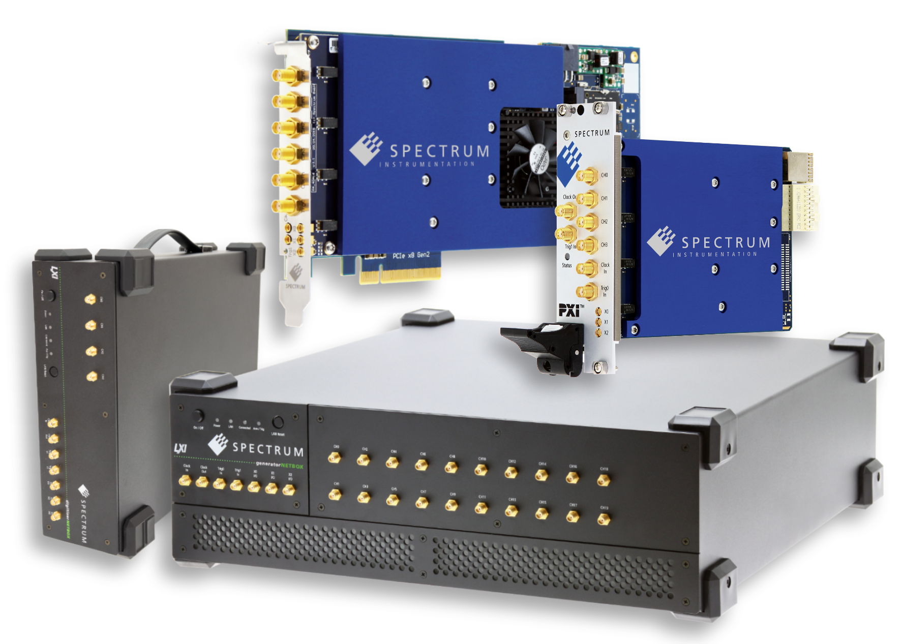 23 different AWGs are able to use the new DDS firmware option. They offer 16-bit resolution, up to 1.25 GS/s speed and up to 32 channels.
The DDS option is available now for the full range of M4i.66xx PCIe cards, M4x.66xx PXIe modules, portable LXI/Ethernet DN2.66x units and multi-channel desktop LXI/Ethernet DN6.66xx products. By simply performing a firmware update, all previously purchased 66xx series products can be equipped with the new firmware option. Programming can be done using the existing driver SDKs that are included in the delivery. Examples are available for Python, C++, MATLAB, LabVIEW and many more. The option is available now.
About Spectrum InstrumentationSpectrum Instrumentation, founded in 1989, uses a unique modular concept to design and produce a wide range of more than 200 digitizers and generator products as PC-cards (PCIe and PXIe) and stand-alone Ethernet units (LXI). In over 30 years, Spectrum has gained customers all around the world, including many A-brand industry-leaders and practically all prestigious universities. The company is headquartered near Hamburg, Germany, known for its 5-year warranty and outstanding support that comes directly from the design engineers. More information about Spectrum can be found at www.spectrum-instrumentation.com
The post DDS Option for high-speed AWGs generates up to 20 sine waves appeared first on ELE Times.
MSTC 2024 to Spotlight Latest MEMS and Sensors Advances Driven by Artificial Intelligence
Keynote speakers at the SEMI MEMS and Sensors Technical Congress (MSTC 2024) will highlight smart home and smart garment innovations driven by artificial intelligence (AI) as industry visionaries and experts gather May 1-2 at Covel Commons at University of California, Los Angeles (UCLA) to discuss the latest MEMS and sensors trends and innovations. Registration is open.
Themed Sensorizing Our World: Technology Driving Global Solutions, MSTC 2024 will feature keynotes and technical sessions on critical MEMS and sensors topics. Highlights also include posters showcasing novel applications from the next generation of innovators and networking opportunities for participants to help grow their businesses.
Sponsored by the SEMI MEMS & Sensors Industry Group (MSIG), MSTC 2024 will offer a deep dive into how to bring sensor products to market, from design through fabrication and testing and packaging to end-use applications. Industry experts will explore the software and systems needed to expand both legacy and emerging MEMS and sensors to open new markets and business opportunities.
MSTC 2024 Keynote Speakers
MSTC 2024 will also showcase MEMS and sensors applications in the following areas:
- AI-driven Sensor Systems
- MEMS Emerging Technology & Devices
- New Frontiers in MEMS & Sensors Fabrication
- Revolutionary Sensors for Biomedical Applications
- Smart Environmental Sensors
- Positioning, Navigation & Timing
- Market and Technology Trends and Forecast
- Automotive Sensor Tech Showdown
- UCLA lab tours
- Networking reception showcasing technology application posters created by students from UCLA
The post MSTC 2024 to Spotlight Latest MEMS and Sensors Advances Driven by Artificial Intelligence appeared first on ELE Times.
300mm Fab Equipment Spending Forecast to Reach Record $137 Billion in 2027, SEMI Reports
Global 300mm fab equipment spending for front-end facilities is forecast to reach a record US$137 billion in 2027 after topping US$100 billion for the first time by 2025 on the strength of the memory market recovery and strong demand for high-performance computing and automotive applications, SEMI highlighted today in its quarterly 300mm Fab Outlook Report to 2027 report.
Worldwide 300mm fab equipment investment is expected to increase 20% to US$116.5 billion in 2025 and 12% to US$130.5 billion in 2026 before hitting a record high in 2027.
“Projections for the steepening ramp of 300mm fab equipment spending in the coming years reflects the production capacity needed to meet growing demand for electronics across a diverse range of markets as well as a new wave of applications spawned by artificial intelligence (AI) innovation,” said Ajit Manocha, SEMI President and CEO. “The newest SEMI report also highlights the critical importance of increases in government investments in semiconductor manufacturing to bolster economies and security worldwide. This trend is expected to help significantly narrow the equipment spending gap between re-emerging and emerging regions and the historical top-spending regions in Asia.”
Regional GrowthThe SEMI 300mm Fab Outlook to 2027 report shows China continuing to lead fab equipment spending with US$30 billion in investments in each of the next four years fueled by government incentives and domestic self-sufficiency policies.
Supported by leading-edge nodes expansion for high-performance computing (HPC) and the memory market recovery, Taiwanese and Korean chip suppliers are increasing their equipment investments. Taiwan is expected to rank second in equipment spending at US$28 billion in 2027, up from US$20.3 billion in 2024, while Korea is expected to rank third at US$26.3 billion in 2027, an increase from US$19.5 billion this year.
The Americas is projected to double 300mm fab equipment investments from US$12 billion in 2024 to US$24.7 billion in 2027, while spending in Japan, Europe & the Middle East, and Southeast Asia are expected to reach US$11.4 billion, US$11.2 billion, and US$5.3 billion in 2027, respectively.
Segment GrowthFoundry segment spending is expected to decline 4% to US$56.6 billion this year due in part to the expected slowdown in mature nodes (>10nm) investment, though the segment continues to log the highest growth among all segments to meet market demand for generative AI, automotive and intelligent edge devices. The segment’s equipment spending is forecast to post a 7.6% compound annual growth rate (CAGR) to US$79.1 billion from 2023 to 2027.
Demand for greater data throughput, crucial for AI servers, is driving strong demand for high-bandwidth memory (HBM) and spurring increased investment in memory technology. Among all segments, memory is ranked second and is expected to post US$79.1 billion in equipment investments in 2027, a 20% CAGR from 2023. DRAM equipment spending is expected to rise to US$25.2 billion in 2027, a 17.4% CAGR, while 3D NAND investment is projected to reach US$16.8 billion in 2027, a 29% CAGR.
The Analog, Micro, Opto, and Discrete segments are projected to increase 300mm fab equipment investments to US$5.5 billion, US$4.3 billion, US$2.3 billion, and US$1.6 billion in 2027, respectively.
The SEMI 300mm Fab Outlook Report to 2027 report lists 405 facilities and lines globally, including 75 high-probability facilities expected to start operation during the four years beginning in 2024. The report reflects 358 updates and 26 new fabs/lines project since its last publication in December 2023.
For more information on the report or to subscribe to SEMI market data, visit SEMI Market Data or contact the SEMI Market Intelligence Team (MIT) at mktstats@semi.org.
The post 300mm Fab Equipment Spending Forecast to Reach Record $137 Billion in 2027, SEMI Reports appeared first on ELE Times.
Infineon to complete limited Share Buyback Program serving fulfillment of obligations under existing employee participation programs
Infineon Technologies AG has successfully completed its Share Buyback Program 2024, announced on 26 February 2024 in accordance with Article 5(1)(a) of Regulation (EU) No 596/2014 and Article 2(1) of Delegated Regulation (EU) No 2016/1052. As part of the Share Buyback Program 2024, a total of 7,000,000 shares (ISIN DE0006231004) were acquired. The total purchase price of the repurchased shares was € 232,872,668. The average purchase price paid per share was € 33.27.
 Alexander Foltin, Head of Finance, Treasury and Investor Relations of Infineon
The buyback was carried out on behalf of Infineon by an independent credit institution via Xetra trading on the Frankfurt Stock Exchange, serving the sole purpose of allocating shares to employees of the company or affiliated companies, members of the Management Board of the company as well as members of the management board and the board of directors of affiliated companies as part of the existing employee participation programs.
The post Infineon to complete limited Share Buyback Program serving fulfillment of obligations under existing employee participation programs appeared first on ELE Times.
UiPath Unveils New Family of LLMs at AI Summit to Empower Enterprises to Harness Full Capabilities of GenAI
Company introduces Context Grounding to augment GenAI models with business-specific data, an IBM watsonx.ai connector, and updates for Autopilot
UiPath, a leading enterprise automation and AI software company, recently announced several new generative AI (GenAI) features in its platform designed to help enterprises realize the full potential of AI with automation by accessing powerful, specialized AI models tailored to their challenges and most valuable use cases. UiPath showcased its latest capabilities at the virtual AI Summit that took place on March 19th, 2024.
The UiPath Business Automation Platform offers end-to-end automation for business processes. There are four key factors that business leaders seeking to embed AI in their automation program must keep top of mind: business context, AI model flexibility, actionability, and trust. The new AI features of the UiPath Platform address these key areas to ensure customers are equipped with the tools necessary to enhance the performance and accuracy of GenAI models and tools and more easily tackle diverse business challenges with AI and automation.
“Businesses need an assortment of AI models, the best in class for every task, to achieve their full potential. Our new family of UiPath LLMs, along with Context Grounding to optimize GenAI models with business-specific data, provide accuracy, consistency, predictability, time to value, and empower customers to transform their business environments with the latest GenAI capabilities on the market,” said Graham Sheldon, Chief Product Officer at UiPath. “These new features ensure that AI has the integrations, data, context, and ability to take action in the enterprise with automation to meet our customers’ unique needs.”
At the AI Summit, UiPath announced:
Generative Large Language Models (LLMs)
The new LLMs, DocPATH and CommPATH, give businesses LLMs that are extensively trained for their specific tasks, document processing and communications. General-purpose GenAI models like GPT-4 struggle to match the performance and accuracy of models specially trained for a specific task. Instead of relying on imprecise and time-consuming prompt engineering, DocPATH and CommPATH provide businesses with extensive tools to customize AI models to their exact requirements, allowing them to understand any document and a huge variety of message types.
Context Grounding to augment GenAI models with business-specific data
Businesses need a safe, reliable, low-touch way to use their business data with AI models. To address this need, UiPath is introducing Context Grounding, a new feature within the UiPath AI Trust Layer that will be entering private preview in April. UiPath Context Grounding helps businesses improve the accuracy of GenAI models by providing prompts and a foundation of business context through retrieval augmented generation. This system extracts information from company-specific datasets, like a knowledge base or internal policies and procedures to create more accurate and insightful responses.
Context Grounding makes business data LLM-ready by converting it to an optimized format that can easily be indexed, searched, and injected into prompts to improve GenAI predictions. Context Grounding will enhance all UiPath Gen AI experiences in UiPath Autopilots, GenAI Activities, and intelligent document processing (IDP) products like Document Understanding.
GenAI Connectors & IBM watsonx.ai
IBM used the UiPath Connector Builder to create a unique watsonx.ai connector. The new connector provides UiPath customers with access to multiple foundational models currently available in watsonx.ai. GenAI use cases, such as summarization, Q&A, task classification, and optimization for chat, are quickly integrated and infused into new and existing UiPath workflows and frameworks. IBM Watsonx customers can also access broader UiPath platform capabilities, such as Test Automation, Process Mining and Studio workflows, all within a low/no-code UX environment. IBM’s industry-leading consulting capabilities, coupled with the UiPath Business Automation Platform, will help support successful GenAI adoption, including the right strategy for infusing AI into more powerful, and complex automated workflows.
“IBM and UiPath strongly believe that AI and GenAI are rapidly changing the entire landscape of business globally,” said Tom Ivory, Senior Partner, Vice President, Global Leader of Global Automation at IBM. “We are excited that IBM’s watsonx.ai and UiPath’s Connector Builder together now help create insights, and efficiencies that result in real value for our customers.”
The IBM Watson Connector is now generally available through the Integration Service Connector Catalog.
Autopilot for Developers and Testers
UiPath Autopilot is a suite of GenAI-powered experiences across the platform that make automation builders and users more productive. Autopilot experiences for Developers and Testers are now available in preview with a targeted general availability in June. Over 1,500 organizations are using UiPath Autopilot resulting in over 7,000 generations and over 5500 expressions generated per week.
Autopilot for Developers empowers both professional and citizen automation developers to create automation, code, and expressions with natural language, accelerating every aspect of building automation.
Autopilot for Testers transforms the testing lifecycle, from planning to analysis, reducing the burden of manual testing and allowing enterprise testing teams to test more applications faster. Autopilot for Testers empowers testing teams to rapidly generate step-by-step test cases from requirements and any other source documents, generate automation from test steps, and surface insights from test results, allowing testers to identify the root cause of issues in minutes, not hours or days.
Prebuilt GenAI Activities for faster time-to-value
New prebuilt GenAI Activities utilize the UiPath AI Trust Layer and are easy to access, develop with, and leverage high-quality AI predictions in automation workflows that deliver faster time to value. GenAI Activities provides access to a growing collection of GenAI use cases, such as text completion for emails, categorization, image detection, language translation, and the ability to filter out personally identifiable information (PII) enabling enterprises to do more with GenAI. With GenAI Activities, enterprises can reduce the time to build and achieve a competitive edge using GenAI to help customize the customer experience, optimize supply chains, forecast demands, and make informed decisions.
The post UiPath Unveils New Family of LLMs at AI Summit to Empower Enterprises to Harness Full Capabilities of GenAI appeared first on ELE Times.
Expanded Semiconductor Assembly and Test Facility Database Tracks OSAT and Integrated Device Manufacturers in 670 Facilities, SEMI and TechSearch International Report
New edition of database tracks 33% more facilities and highlights advanced packaging and factory certifications
The new edition of the Worldwide Assembly & Test Facility Database expands coverage to 670 facilities, 33% more than the previous release, including 500 outsourced semiconductor assembly and test (OSAT) service providers and 170 integrated device manufacturer (IDM) facilities, SEMI and TechSearch International announced today. The database is the only commercially available listing of assembly and test suppliers that provides comprehensive updates on packaging and testing services offered by the semiconductor industry.
The updated database includes factory certifications in critical areas such as quality, environmental, security and safety as well as data reflecting automotive quality certifications obtained by each site. The new edition also highlights advanced packaging offerings by each factory, defined as flip chip bumping and assembly, fan-out and fan-in wafer-level packaging (WLP), through silicon via (TSV), 2.5D and 3D capability.
“Understanding the location of legacy packaging as well as advanced packaging and test is essential to effective supply-base management,” said Jan Vardaman, President at TechSearch International. “The updated Worldwide Assembly & Test Facility Database is an invaluable tool in tracking the packaging and assembly ecosystem.”
“The database increases its focus on advanced packaging while highlighting conventional packaging capabilities and new test capabilities to support innovations in key end markets including automotive,” said Clark Tseng, Senior Director of SEMI Market Intelligence.
Combining the semiconductor industry expertise of SEMI and TechSearch International, the Worldwide Assembly & Test Facility Database update also lists revenues of the world’s top 20 OSAT companies and captures changes in technology capabilities and service offerings.
Covering facilities in the Americas, China, Europe, Japan, Southeast Asia, South Korea and Taiwan, the database highlights new and emerging packaging offerings by manufacturing locations and companies. Details tracked include:
- Plant site location, technology, and capability: Packaging, test, and other product specializations, such as sensor, automotive and power devices
- Packaging assembly service offerings Ball grid array (BGA), specific leadframe types such as quad flat package (QFP), quad flat no-leads (QFN), small outline (SO), flip-chip bumping, WLP, Modules/System in Package (SIP), and sensors
- New manufacturing sites announced, planned or under construction
Key Report Highlights
- The world’s top 20 OSAT companies in 2022 with financial comparisons to 2021, as well as preliminary comparisons to 2023
- 150-plus facility additions compared to the 2022 report
- 200-plus companies and more than 670 total back-end facilities
- 325-plus facilities with test capabilities
- 100-plus facilities offering QFN
- 85-plus bumping facilities, including more than 65 with 300mm wafer bumping capacity
- 90-plus facilities offering WLCSP technology
- 130-plus OSAT facilities in Taiwan, more than 150 in China, and more than 60 in Southeast Asia
- 50-plus IDM assembly and test facilities in Southeast Asia, about 45 in China, nearly 20 in Americas and more than 12 in Europe
- More than 30% of global factories offering advanced packaging capabilities in one of the following areas: flip chip bumping and assembly, fan-out and fan-in WLP, TSV, 2.5D and 3D
Worldwide Assembly & Test Facility Database licenses are available for single and multiple users. SEMI members save up to 25% on licenses. Download a sample of the report and see pricing and ordering details.
For more information on the database or to subscribe to SEMI market data, visit SEMI Market Data or contact the SEMI Market Intelligence Team (MIT) at mktstats@semi.org.
The post Expanded Semiconductor Assembly and Test Facility Database Tracks OSAT and Integrated Device Manufacturers in 670 Facilities, SEMI and TechSearch International Report appeared first on ELE Times.
STM32 Summit: 3 important embedded systems trends for 2024
Author: STMicroelectronics
Where are embedded systems heading in 2024, and how can makers stay ahead of the curve? Few people used to ask these questions a decade ago. Today, the answers can make or break entire companies. Indeed, once relegated to a few niche applications, embedded systems are now everywhere. From factories to home appliances or from expensive medical devices in hospitals to ubiquitous wearables, every time we become more connected or more sustainable, an embedded system is usually at the heart of innovations. ST will thus hold the STM32 Summit on March 19 to introduce our community to the latest technologies shaping our industry. In the meantime, let’s step back to see where 2024 is taking us.
Computational efficiency or doing more with lessAvid readers of the ST Blog know that greater efficiency is often a key driver of our innovations. However, we may need to broaden our understanding of “efficiency”. In essence, efficiency is the ratio of work done per amount of energy spent. In the microcontroller world, it refers to electrical efficiency. Hence, improving efficiency means lowering the power consumption while offering the same or more computational throughput. However, as embedded systems applications become vastly more optimized, a new efficiency ratio shapes the industry: application complexity for a given computational throughput.
To illustrate this point, let’s use a simple thought experiment. Imagine bringing today’s high-performance MCU back in time just five years ago. That device could not run the neural network or rich UIs it can run today because frameworks and machine learning algorithms were far cruder. The reason is that embedded systems aren’t just more powerful but that new applicative optimizations have made them more capable. Consequently, the same amount of computational power yields far greater results today.
 Trained vs. pruned and quantized with TAO Toolkit
For instance, the quantization of neural networks enabled more powerful edge AI systems. In the case of a recent demo with Schneider Electric, a deeply quantized neural network meant that a people-counting application ran on an STM32H7. And NVIDIA featured the same MCU when running a network optimized with its TAO Toolkit and STM32Cube.AI. Similarly, new motor control algorithms, like ZeST, mean MCUs drive motors more accurately and efficiently, and new UI framework optimizations mean richer graphics while needing less memory. For instance, the latest version of TouchGFX supports vector fonts, and our latest STM32U5 has an IP accelerating vector graphics, which wouldn’t have been as impressive without the graphical framework to help developers take advantage of it.
Consequently, engineers must not only ensure their embedded processing solutions is reducing their power consumption but that it also runs the latest optimizations. In many instances, a real-time application is no longer just basic code running in a while loop. Developers must find new ways to leverage the cloud, machine learning, sensor fusion, or graphical interfaces. Hence, it is critical to find the right MCU supported by an entire ecosystem that can bring these new optimizations to them. Engineers must ask how fast a device runs and how well it can support the complexity and richness of the application.
Multiple wireless protocol support or talking more with the world A wireless utility metering system
The idea that an embedded system connects to a network is far from new. The industry even coined the term “Internet of Things” because so many applications rely on the network of networks. However, until now, applications have primarily chosen one mode of communication, either wired or wireless. And if the latter, it used to settle on one wireless protocol, such as cellular, Wi-Fi, or Bluetooth. Over the years, the industry has seen the multiplication of wireless protocols. From 6LoWPAN to LoRaWAN, Zigbee, Thread, NB-IoT, and more, there’s no shortage of new protocols. Interestingly, there has also been the absence of a clear winner. Instead of a traditional consolidation, many technologies seem to prosper concomitantly.
Let’s take the 2.4 GHz spectrum as an example. While Bluetooth is still dominant, Zigbee and Thread have grown in popularity. Many companies also work on a custom IEEE 802.15.4 protocol for competitive or regulatory reasons. In fact, the proliferation of network protocols is so rampant that Matter, the latest initiative unifying home automation under one standard, runs over multiple wireless technologies like Wi-Fi, Thread, and Bluetooth and supports many 2.4 GHz bridges, including Zigbee and Z-Wave instead of settling on just one wireless technology.
As a result, engineers face a relatively new challenge: create a system that must support multiple wireless protocols to stay competitive. Indeed, by adopting a device that supports multiple technologies, a company can qualify one MCU and adapt to the needs of the market. For instance, a developer could work on a proprietary IEEE 802.15.4 protocol in one region, and then adopt Thread in another while keeping the exact same hardware. It would only require a change to the code base. Engineers would thus reduce their time to market and enjoy far greater flexibility. Put simply, embedded systems developers in 2024 must design with multi-protocol support in mind and choose devices that will meet current and future needs.
Security or protecting future investments Security must be a top priority for smart home products
One positive trend in embedded systems has been recognizing that security is not optional. For the longest time, many joked that IoT stood for “Internet of Threats”. Today, developers know it is imperative to protect servers, code, end-user data, and even physical devices from attacks. In a nutshell, a failure to secure an embedded system could have catastrophic effects on the product and its brand. However, a new security challenge has emerged in the form of regulatory interventions. The European Union, the United States, and many other countries and standardizing bodies have enacted new rules mandating features and protections. The problem is that they aren’t always clear or final, as some are still being worked on.
The industry has been answering this new challenge with more formal security standards. For instance, the Platform Security Architecture (PSA) and the Security Evaluation Standard for IoT Platforms (SESIP) certifications offer an extensive methodology to help engineers secure their embedded systems. These certifications thus provide a path to future-proof designs and ensure they meet any stringent requirements. However, it also means that developers can’t treat security as an afterthought or work toward those certifications after designing their system. It is becoming critical to think of security as soon as the first proof of concept and adopt a microcontroller that can meet the proper certification level.
Let’s take the example of a smart home application that shares private and sensitive data with a cloud. Increasingly, governments require encrypted communications, protections against physical attacks, safeguards against software intrusions, the ability to securely update a system over-the-air, and monitoring capabilities to detect a breach. In many instances, a SESIP Level 3 certification would help guarantee that a system could meet those requirements. Unfortunately, engineers who fail to choose an MCU capable of targeting such a certification could end up compromising the entire project. As there are hardware and platform considerations that ensure a product can meet a certain security certification, developers must adopt a new mindset when choosing an MCU.
See what the future holds at the STM32 Summit See how the STM32 Summit can help you anticipate upcoming trends
As we look at the trends that will shape 2024 and beyond, we see that it is critical to find an ecosystem maker. Computational efficiency depends on the MCU as well as the framework, middleware, and algorithms that run on it. Similarly, supporting multiple wireless protocols demands new development tools, and securing embedded systems requires practical software solutions on top of hardware IPs. That’s why we are excited to host the STM32 Summit on March 19. Join us as we showcase how ST is bringing solutions to help teams stay ahead of upcoming trends.
Viewers will get to learn more about exciting devices that are shaping new trends while also discovering entirely new products. Attendees will also be able to ask questions to ST experts and receive answers live. Registering to this event thus grants a unique access to our teams. Moreover, the STM32 Summit will feature some of our customers who will share real-world experiences. Instead of ST telling the industry how to meet the challenges ahead, we wanted our partners to show viewers how they do it. Put simply, the STM32 Summit isn’t only here to inform but to inspire.
The post STM32 Summit: 3 important embedded systems trends for 2024 appeared first on ELE Times.
u-blox launches new GNSS platform for enhanced positioning accuracy in urban environments
The u-blox F10 platform increases positioning accuracy by reducing multipath effects, simplifying the process of promptly locating a vehicle.
u-blox, a global provider of leading positioning and wireless communication technologies and services, has announced F10, the company’s first dual-band GNSS (Global Navigation Satellite Systems) platform combining L1 and L5 bands to offer enhanced multipath resistance and meter-level positioning accuracy. The platform caters to urban mobility applications, such as aftermarket telematics and micromobility.
Applications that use GNSS receivers for accurate positioning are on the rise. Yet, current receivers do not fully perform in urban areas. Accurate and reliable positioning in dense urban environments, where buildings or tree foliage can reflect satellite signals, requires GNSS receivers to mitigate multipath effects. The L5 band’s resilience to these effects significantly improves positioning accuracy. Combined with the well-established L1 band, an L1/L5 dual-band GNSS receiver can deliver < 2 m positioning accuracy (CEP50), against about 4 m with the L1 band only. The u-blox team has conducted driving tests in several urban areas, confirming a significant improvement over GNSS L1 receivers.
The F10’s firmware algorithm prioritizes L5 band signals in weak signal environments, ensuring reliable positioning accuracy even when paired with small antennas. The platform is also equipped with protection-level technology that provides a real-time trustworthy positioning accuracy estimate.
When a cellular modem is extremely close to a GNSS receiver, it can interfere with the receiver’s reception. Some F10 module models (NEO-F10N, MAX-F10S, and MIA-F10Q) are equipped with a robust RF circuit that allows the GNSS and the cellular modem to operate without interference.
The u-blox F10 platform is pin-to-pin compatible with the previous u-blox M10 generation for easy migration. It also supports u-blox AssistNow, which offers real-time online A-GNSS service with global availability to reduce GNSS time-to-first-fix and power consumption.
The u-blox EVK-F101 evaluation kit will be available in April 2024.
The post u-blox launches new GNSS platform for enhanced positioning accuracy in urban environments appeared first on ELE Times.
Looking into CDN Traffic in the Network
A CDN or Content Delivery Server, is a geographically distributed network of interconnected servers. CDNs are a crucial part of the modern internet infrastructure which solves the problem of latency (delay before transfer of data begins from a web server) by speeding up the webpage loading time for data-heavy (like multimedia) web applications.
The usage of CDN has significantly increased with the rise of data volumes in web applications in the last few years. As per the Sandvine Global Internet Phenomena Report 2023, different popular CDN providers are included in the list of top 10 video applications for APAC region for their increased volume of application traffic.
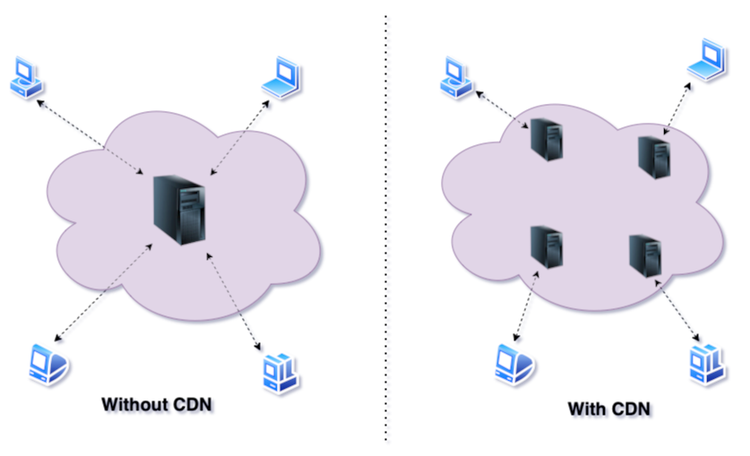 Figure 1: Without CDN and with CDN scenario
Network Traffic Analysis
Figure 1: Without CDN and with CDN scenario
Network Traffic Analysis
The ATI team in Keysight has analyzed the network traffic of different popular CDN like Amazon CloudFront, Cloudflare, Akamai, Fastly and has seen some interesting information from the decrypted traffic which can be useful for other researchers.
Inside HTTP Request Header:When a website decides to use CDN, then sometimes it typically integrates the CDN service name like CloudFront, Cloudflare, akamai etc. at the DNS level which changes the DNS records like CNAME records to point into the CDN’s domain. The same behavior is also seen inside the “Host” or “: authority” header inside the HTTP request. For example, if the original website is “www. popularOTT.com”, then after the CDN name integration the URL looks like www.popularOTT.cdnprovider.com as shown below –
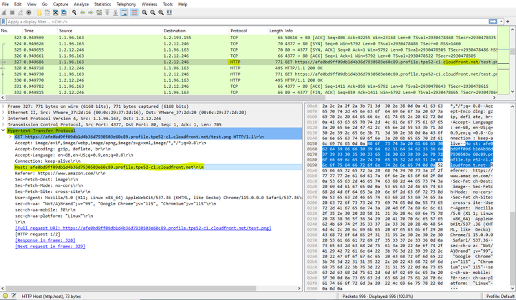 Figure 2: Sample CDN request header
Inside HTTP Response Header:
Figure 2: Sample CDN request header
Inside HTTP Response Header:
When a response is sent from the Content Delivery Server (CDN) server, it often includes some specific headers inside the HTTP response packet which provide some information about the CDN server as shown below –
- X-Cache: This header indicates whether a request is a hit, miss or bypass in the CDN cache. If its value is set as “HIT” (“HIT from cloudfront” for CloudFront) inside the HTTP response that means the request is served by the CDN server, not the origin server.
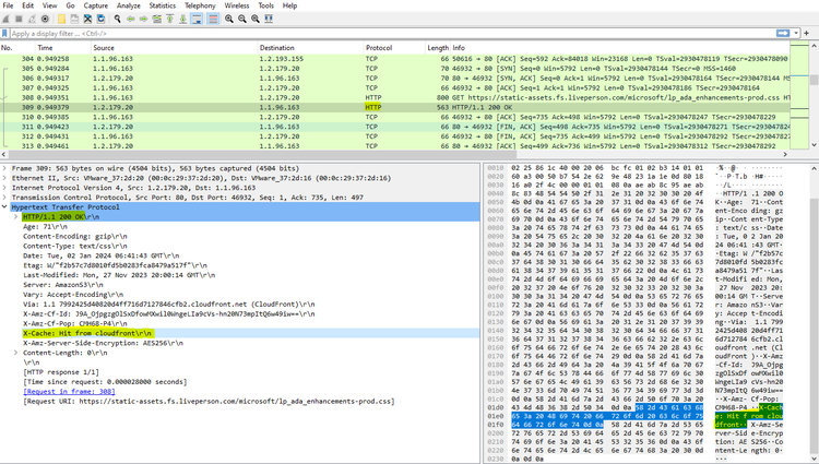 Figure 3: Sample response header from CDN server containing X-Cache header.
- X-Cache-Status: It is similar to “X-Cache” header which provides some detailed information about the caching process. Sometimes we also see the CDN provider information inside the header name. As example when a response is sent from Cloudflare CDN, then sometimes we see this “cf-cache-status” (here cf refers to Cloudflare) header inside the response packet.
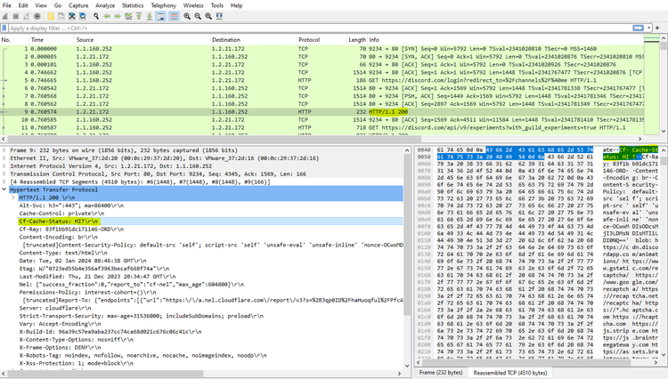 Figure 4: Sample response header from CDN server containing X-Cache-Status header.
- Via: This repones header indicates if any intermediate proxy or CDN presents through which the request has passed. As example when a request has passed through Amazon CloudFront CDN, then sometimes we see information about that like “1 2b14bcf8de4af74db0f6562ceac643f8.cloudfront.net (CloudFront)” inside the “via” response header.
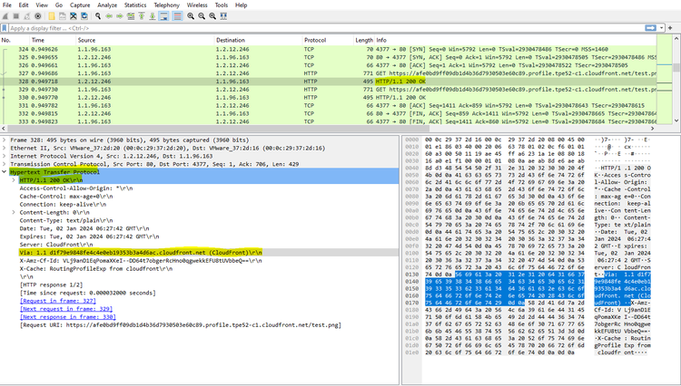 Figure 5: Sample response header from CDN server containing Via header.
- Server: In some cases, we can see the CDN server name in the “server” header inside the HTTP response packet as shown below –
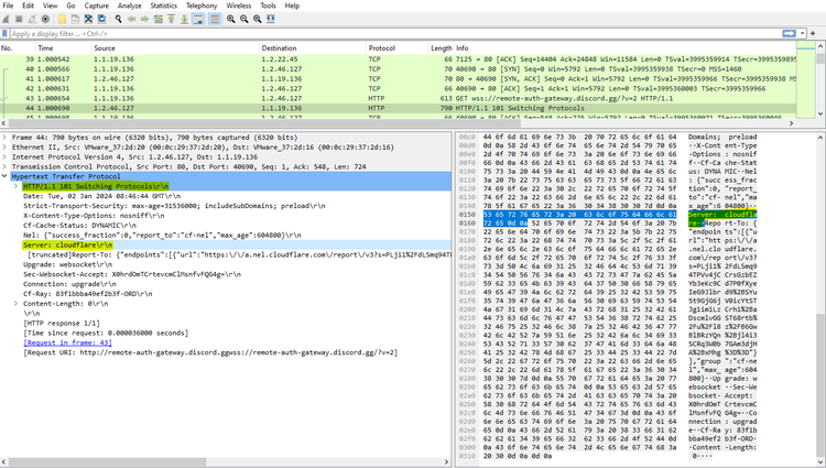 Figure 6: Sample response header from CDN server containing Server header.
- Sometimes, we see other custom headers like “x-akamai-request-id”, “x-bdcdn-cache-status” etc. inside the HTTP response which indicates that the response is sent from a CDN server.
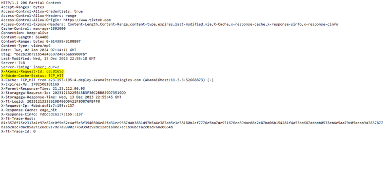 Figure 7: Sample response header from CDN server containing other CDN related headers.
CDN in Keysight ATI
At Keysight Technologies, our Application and Threat Intelligence (ATI) team, researchers have examined the traffic pattern of various leading CDN service providers based on their application traffic from the world’s top 50 most popular websites and they have published the network traffic pattern of 2 popular CDNs (Amazon CloudFront and Cloudflare) in ATI-2024-03 Strike Pack released on February 15, 2024. So please stay tuned for the other popular CDN application traffic which will be released in the upcoming ATI releases.
The post Looking into CDN Traffic in the Network appeared first on ELE Times.
Digital Twins and AI Acceleration Are Transforming System Design
We are at a global inflection point as we cope with the limitations of energy supply and the consequences of climate change. Regional conflicts are elevating risks in the traditional crude oil supply chain. Changes in rainfall patterns and disputes over water use priorities are limiting hydroelectric power generation. Moreover, extreme weather events have intensified the threat to lives and property. These challenges are compelling us to focus on energy efficiency requirements in almost everything we do. As a result, there is a significant trend towards designing more energy-efficient transportation and generation equipment.
Designing Energy-Efficient MachineryEach industry has its goals to respond to these trends. The automotive industry is investing in electric vehicles and enhancing the aerodynamic efficiency of all their vehicles. The aerospace industry aims to reduce the cost and time required to design new aircraft models that are efficient and durable. In the same vein, the turbomachine industry benefits significantly from every efficiency and extension improvement of the product lifecycle.
 Figure 1: OEM Design Goals
Automotive Design
Figure 1: OEM Design Goals
Automotive Design
The automotive industry must comply with the new CAFÉ standards for 2028 and 2032. These standards will have an impact on their fleet, meaning they will need to build electric vehicles and improve the average fuel efficiency for their internal combustion engine models. A 10% reduction in the aerodynamic drag coefficient can lead to a 5% improvement in fuel economy. Simulation is a crucial tool to ensure that the design will perform well once manufactured and tested in the wind tunnel.
 Figure 2: Automotive Design for Fuel Efficiency
To achieve this kind of leap forward, the industry must be able to do the following:
- Simulate turbulent air in fine detail
- Evaluate 100s of precise aerodynamic design changes
- Simulate entire car design for net impact
The commercial aircraft industry is highly regulated with a focus on safety and environmental impact. The process of designing a new aircraft involves several steps that must meet requirements for safe function, performance, and operation, and the aircraft must be certified for the entire flight envelope. Simulation is the only way to ensure the aircraft will perform as intended before building and flight-testing a prototype.
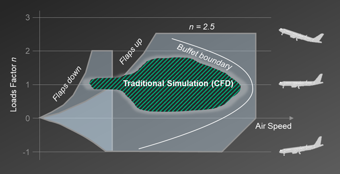 Figure 3: Aerospace Flight Envelope Performance
To simulate all operating conditions, designers must:
- Simulate lift in turbulent air in fine detail
- Simulate the entire aircraft design for net impact
- Evaluate all operating conditions (see chart)
Turbomachinery includes energy generators, large turbine aircraft engines, marine engines, and other machines with rotating motion. Improving energy efficiency can yield significant returns because of the scaled impact of the machine over its lifetime. Similarly, designing machines to last longer and require less maintenance can have a significant economic impact. Simulation is the best way to analyze various design changes to optimize the final design outcome.
 Figure 4: Turbomachinery Design for Efficiency and Durability
To achieve this kind of leap forward, the industry must be able to:
- Evaluate multiple design optimization tradeoffs
- Simulate combustion dynamics in fine detail
- Simulate a full engine design for net impact
To address these needs, we are announcing the world’s first accelerated digital twin, delivering unprecedented performance and energy efficiency—the Cadence Millennium Enterprise Multiphysics Platform. Targeted at one of the biggest opportunities for greater performance and efficiency, the first-generation Cadence Millennium M1 CFD Supercomputer accelerates high-fidelity computational fluid dynamics (CFD) simulations. Available in the cloud or on-premises, this turnkey solution includes graphics processing units (GPUs) from leading providers, extremely fast interconnections, and an enhanced Cadence high-fidelity CFD software stack optimized for GPU acceleration and generative AI. By fusing Millennium M1 instances into a unified cluster, customers can achieve an unprecedented same-day turnaround time and near-linear scalability when simulating complex mechanical systems.
The Millennium Platform addresses the performance and efficiency needs of the automotive, aerospace and defense (A&D), energy, and turbomachinery industries with critical advances in multiphysics simulation technology. Performance, accuracy, capacity, and accelerated computing are all essential to enabling digital twin simulations that explore more design innovations, providing confidence that they will function as intended before undertaking prototype development and testing.
Highlights and benefits include:
- Performance: Combines best-in-class GPU-resident CFD solvers with dedicated GPU hardware to provide supercomputer-equivalent throughput per GPU of up to 1000 CPU cores
- Efficiency: Reduces turnaround time from weeks to hours with 20X better energy efficiency compared to its CPU equivalent
- Accuracy: Leverages Cadence Fidelity CFD solvers to provide unmatched accuracy to address complex simulation challenges
- High-Performance Computing: Built with extensible architecture and massively scalable Fidelity solvers to provide near-linear scalability on multiple GPU nodes
- AI Digital Twin: Rapid generation of high-quality multiphysics data enables generative AI to create fast and reliable digital twin visualizations of the optimal system design solution
- Turnkey Solution: The industry’s first solution that couples GPU compute with modern and scalable CFD solvers, providing an optimized environment for accelerated CFD and multidisciplinary design and optimization
Flexibility: Available with GPUs from leading vendors, in the cloud with a minimum 8-GPU configuration or on-premises with a minimum 32-GPU configuration—providing a flexible and scalable solution to fit each customer’s deployment needs
The post Digital Twins and AI Acceleration Are Transforming System Design appeared first on ELE Times.
The Critical Role of Constraint-Based PCB Design in Modern Electronics (PCB Design)
Welcome to the intricate realm of PCB (Printed Circuit Board) design, where what begins as a simple circuit board evolves into a sophisticated masterpiece of electronic engineering. As the backbone of modern electronics, PCBs breathe life into our everyday devices, from smartphones to laptops. Crafting a reliable and functional PCB extends beyond merely connecting components. It demands a meticulous understanding of various aspects to achieve optimal performance and manufacturability. Central to this endeavor is constraint-based PCB design—a strategic methodology that meticulously governs the physical and electrical characteristics of a PCB. Such constraints not only safeguard against manufacturing pitfalls but also ensure electrical prowess, culminating in a product that doesn’t just meet the mark but sets new standards. In this post, we explore PCB constraints and how they play a crucial role in ensuring a successful design.
Grasping Constraint-Based PCB Design
Constraint-based design involves defining parameters that dictate how a PCB should be constructed. These constraints encompass multiple aspects, including electrical, physical, and manufacturing considerations. Considering constraints early in the design process is crucial, as it sets the groundwork for a successful design that aligns with the project requirements and end goals.
Constraint-based PCB design is akin to a maestro orchestrating a symphony. It balances numerous requirements to shape the overall design process, ensuring a harmonious outcome. These constraints can vary:
Electrical Constraints:- Trace Width and Spacing:Defines the width and spacing of traces to ensure proper current carrying capacity and avoid short-circuits.
- Via Sizes and Types:Specifies dimensions and types of vias, based on design requirements and manufacturing capabilities.
- Impedance Control:Ensures traces are designed to have specific impedance values, crucial for high-speed designs.
- Clearance:Defines the minimum distance between different electrical entities (like traces, pads, vias) to avoid short circuits.
- High-speed Constraints:Rules related to the design of high-speed circuits, including length matching, differential pair routing, and phase control.
- Board Dimensions:Specifies the size and shape of the PCB.
- Layer Stackup:Defines the number and arrangement of copper and insulating layers in the PCB.
- Component Placement:Provides guidelines for placing components on the board, ensuring they don’t interfere with each other and adhere to thermal and mechanical considerations.
- Thermal Constraints:Ensures areas generating high heat have sufficient thermal relief, including the use of heat sinks or thermal vias.
- Solder Mask Clearance:Ensures that solder masks are appropriately applied to avoid short circuits during the soldering process.
- Silkscreen Overlap:Ensures that component labels or other silkscreen elements do not overlap with pads or vias.
- Hole Sizes:Specifies the minimum and maximum sizes for drilled holes based on manufacturing capabilities.
- Annular Ring Size:Defines the minimum width of the copper ring around a drilled hole.
- Copper-to-Edge Clearance:Defines the minimum distance required between the edge of the PCB and any copper feature.
- Component Orientation:Ensures components are correctly oriented for automated assembly.
- Component-to-Component Clearance:Ensures sufficient space between components to allow for assembly and avoid interference.
- Polarity and Pin 1 Indicators:Guidelines for marking components to ensure they are placed correctly during assembly.
- Flex and Bend: Defines regions that can and cannot be bent in flex PCBs.
- Vibration and Shock: Constraints to ensure components can withstand specific vibration and shock levels, especially in rugged applications.
- Testing Constraints (Design for Test – DFT):
- Test Point Requirements:Specifies the number and placement of test points for in-circuit testing.
- Access for Probing:Ensures test equipment can access critical nodes during testing.
- Environmental and Regulatory Constraints:
- RoHS/Lead-Free Design:Ensures PCBs are designed to adhere to environmental regulations, like the Restriction of Hazardous Substances (RoHS).
- Electromagnetic Compatibility (EMC):Ensures designs adhere to electromagnetic interference (EMI) and susceptibility requirements.
A. Enhanced Signal Integrity and Reliability
In the world of electronics, signal integrity is paramount. Constraint-based design minimizes electromagnetic interference (EMI) and ensures proper trace routing for impedance control. By optimizing ground and power planes, noise is reduced, leading to improved signal reliability.
B. Improved Thermal Management
Efficient heat dissipation is a challenge in compact electronics. Constraint-based design tackles this by strategically placing components, utilizing thermal relief, and integrating sensors for real-time temperature monitoring. This ensures that devices maintain optimal operating temperatures.
C. Streamlined Manufacturing and Assembly
Designing for manufacturability (DFM) is a key concept. Constraint-based design includes component placement rules that facilitate automated assembly, reducing errors. By considering various soldering and assembly techniques, manufacturing becomes more seamless.
D. Faster Time-to-Market
Time is of the essence in the competitive electronics market. Constraint-based design reduces the need for countless design iterations by identifying flaws early through simulations. Collaborative design involving cross-functional teams also expedites the process.
E. Cost Savings
Design re-spins are expensive and time-consuming. Constraint-based design minimizes these by ensuring the initial design aligns with requirements. Efficient layouts optimize material usage and eliminate the need for costly post-production modifications.
F. Compliance and Standards
Electronic products must adhere to regulatory standards. Constraint-based design aids in designing with EMC, safety, and other industry standards in mind. This simplifies the certification process and ensures products meet legal requirements.
Implementing the MethodologyDesign Rule Check (DRC) is a fundamental step in the PCB design process. It involves checking the design against a set of predefined rules to ensure the PCB will be functional, manufacturable, and reliable. Implementing DRC in your PCB design process helps catch errors before manufacturing, reducing costly re-spins, and potential functional issues.
Here’s a step-by-step guide on how to implement DRC in PCB design:- Understand Manufacturing Capabilities:
- Begin by gathering the capabilities and constraints from your PCB manufacturer. This might include rules related to trace width and spacing, via sizes, hole sizes, annular ring sizes, and whatever you need to set your design up for success.
- Set Up the Design Rules in Your PCB Design Software:
- Most modern PCB design tools include a design rules setup or configuration section;
- Enter the manufacturer’s constraints and any additional rules you need for your specific design. This might include electrical rules, high-speed rules, thermal rules, etc.
- Layer-specific Rules:
- Some rules are specific to certain layers. For example, the top and bottom layers might have different trace width and spacing rules compared to inner layers. Make sure to define these layer-specific rules.
- Run the DRC:
- Once your rules are set up, you can run the DRC. This will usually generate a list of violations or errors based on the rules you’ve set;
- Some common violations might include trace width violations, clearance violations, unconnected nets, and overlapping components.
- Review and Address Violations:
- For each violation, the PCB design software typically provides a description and a visual indication of where the issue is on the board;
- Go through each violation and correct the issue in the design. This might involve moving components, rerouting traces, or adjusting the design rules if they were set up incorrectly.
- Iterative Process:
- After correcting known violations, run the DRC again to ensure that no new issues have been introduced and all previous ones have been resolved;
- This might need to be repeated several times until no violations are found.
- Additional Checks:
- Beyond standard DRC, consider running other checks like Electrical Rule Check (ERC) to catch logical and connectivity errors, or a Differential Pair Routing Check for high-speed designs.
- Document Any Deliberate Violations:
- In some cases, you might choose to violate a rule deliberately for a specific design requirement. In such cases, it’s essential to document this decision, explaining the rationale and ensuring the manufacturer is aware of it.
- Collaborate with the Manufacturer:
- Before finalizing the design, it can be beneficial to send the design files to the manufacturer for review. They might run their own DRC and provide feedback based on their specific manufacturing processes.
- Stay Updated:
- Manufacturing capabilities and standards can change over time. Periodically review and update your design rules to ensure they align with the latest capabilities and industry best practices.
The world of electronics is in perpetual flux, with innovations emerging at breakneck speeds. Amidst this, constraint-based PCB design emerges as a beacon, illuminating the path for designers. By meticulously defining, applying, and validating constraints, designers can craft PCBs that aren’t just functional but also efficient, cost-effective, and superior in quality. In an age where precision and speed are paramount, can you afford to design any other way?
Sr. Technical Marketing Engineer
Altium
The post The Critical Role of Constraint-Based PCB Design in Modern Electronics (PCB Design) appeared first on ELE Times.
What is an NPU? And why is it key to unlocking on-device generative AI?
The generative artificial intelligence (AI) revolution is here. With the growing demand for generative AI use cases across verticals with diverse requirements and computational demands, there is a clear need for a refreshed computing architecture custom-designed for AI. It starts with a neural processing unit (NPU) designed from the ground-up for generative AI, while leveraging a heterogeneous mix of processors, such as the central
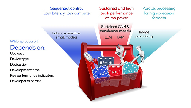 Figure 1: Choosing the right processor, like choosing the right tool in a toolbox, depends on many factors and enhances generative AI experiences.
processing unit (CPU) and graphics processing unit (GPU). By using an appropriate processor in conjunction with an NPU, heterogeneous computing maximizes application performance, thermal efficiency and battery life to enable new and enhanced generative AI experiences.
Why is heterogenous computing important?Because of the diverse requirements and computational demands of generative AI, different processors are needed. A heterogeneous computing architecture with processing diversity gives the opportunity to use each processor’s strengths, namely an AI-centric custom-designed NPU, along with the CPU and GPU, each excelling in different task domains. For example, the CPU for sequential control and immediacy, the GPU for streaming parallel data, and the NPU for core AI workloads with scalar, vector and tensor math.
Heterogeneous computing maximizes application performance, device thermal efficiency and battery life to maximize generative AI end-user experiences.
 Figure 2: NPUs have evolved with the changing AI use cases and models for high performance at low power.
What is an NPU?
Figure 2: NPUs have evolved with the changing AI use cases and models for high performance at low power.
What is an NPU?
The NPU is built from the ground-up for accelerating AI inference at low power, and its architecture has evolved along with the development of new AI algorithms, models and use cases. AI workloads primarily consist of calculating neural network layers comprised of scalar, vector,and tensor math followed by a non-linear activation function. A superior NPU design makes the right design choices to handle these AI workloads and is tightly aligned with the direction of the AI industry.
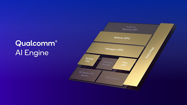 Figure 3: The Qualcomm AI Engine consists of the Qualcomm Hexagon NPU, Qualcomm Adreno GPU, Qualcomm Kryo or Qualcomm Oryon CPU, Qualcomm Sensing Hub, and memory subsystem.
Our leading NPU and heterogeneous computing solution
Figure 3: The Qualcomm AI Engine consists of the Qualcomm Hexagon NPU, Qualcomm Adreno GPU, Qualcomm Kryo or Qualcomm Oryon CPU, Qualcomm Sensing Hub, and memory subsystem.
Our leading NPU and heterogeneous computing solution
Qualcomm is enabling intelligent computing everywhere. Our industry-leading Qualcomm Hexagon NPU is designed for sustained, high-performance AI inference at low power. What differentiates our NPU is our system approach, custom design and fast innovation. By custom-designing the NPU and controlling the instruction set architecture (ISA), we can quickly evolve and extend the design to address bottlenecks and optimize performance.
The Hexagon NPU is a key processor in our best-in-class heterogeneous computing architecture, the Qualcomm AI Engine, which also includes the Qualcomm Adreno GPU, Qualcomm Kryo or Qualcomm Oryon CPU, Qualcomm Sensing Hub, and memory subsystem. These processors are engineered to work together and run AI applications quickly and efficiently on device.
Our industry-leading performance in AI benchmarks and real generative AI applications exemplifies this. Read the whitepaper for a deeper dive on our NPU, our other heterogeneous processors, and our industry-leading AI performance on Snapdragon 8 Gen 3 and Snapdragon X Elite.
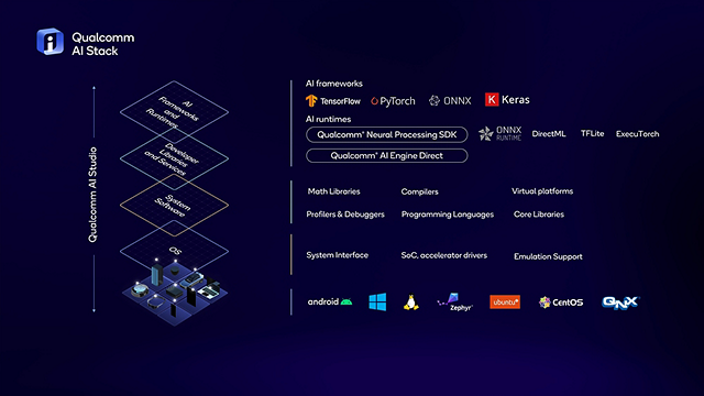 Figure 4: The Qualcomm AI Stack aims to help developers write once and run everywhere, achieving scale.
Enabling developers to accelerate generative AI applications
Figure 4: The Qualcomm AI Stack aims to help developers write once and run everywhere, achieving scale.
Enabling developers to accelerate generative AI applications
We enable developers by focusing on ease of development and deployment across the billions of devices worldwide powered by Qualcomm and Snapdragon platforms. Using the Qualcomm AI Stack, developers can create, optimize and deploy their AI applications on our hardware, writing once and deploying across different products and segments using our chipset solutions.
The combination of technology leadership, custom silicon designs, full-stack AI optimization and ecosystem enablement sets Qualcomm Technologies apart to drive the development and adoption of on-device generative AI. Qualcomm Technologies is enabling on-device generative AI at scale.
 DURGA MALLADI SVP & GM, Technology Planning & Edge Solutions, Qualcomm Technologies, Inc.
 PAT LAWLOR
Director, Technical Marketing,
Qualcomm Technologies, Inc.
The post What is an NPU? And why is it key to unlocking on-device generative AI? appeared first on ELE Times.
Boost AI Projects on Google Cloud Platform using Intel Cloud Optimization Modules
Courtesy: Intel
Applications powered by artificial intelligence are some of the most popular pieces of software being developed, especially on cloud computing platforms, which can provide easy access to specified hardware and accelerators at a low startup cost with the option to scale effortlessly. A popular cloud service provider, Google Cloud Platform* (GCP), contains a suite of cloud computing services that provide a variety of tools to develop, analyze, and manage data and applications. GCP also includes tools specific to AI and machine learning development, such as the AI Platform, the Video Intelligence API, and the Natural Language API. Using a platform like GCP for your AI projects can simplify your development while gaining access to powerful hardware that meets your specific needs.
Further enhancements to model efficiency can be accomplished with pre-built software optimizations tailored for diverse applications. By implementing these software optimizations, developers can see models deploy and infer faster and with fewer resources. However, the process of discovering and integrating these optimizations into workflows can be time-consuming and demanding. Accessing comprehensive guides and documentation packaged in an open-source environment empowers developers to overcome challenges by incorporating new optimizing architectures, facilitating the effortless enhancement of their models’ performance.
What are Intel Cloud Optimization Modules?The Intel Cloud Optimization Modules consist of open-source codebases that feature codified Intel AI software optimizations designed specifically for AI developers working in production environments. These modules provide a set of cloud-native reference architectures to enhance the capabilities of AI-integrated cloud solutions. By incorporating these optimization solutions, developers can boost the efficiency of their workloads and ensure optimal performance on Intel CPU and GPU technologies.
These cloud optimization modules are available on several highly popular cloud platforms, including GCP. The modules utilize specifically built tools and end-to-end AI software and optimizations that enhance workloads on GCP and increase performance. These optimizations can increase machine learning models for a variety of use cases, such as Natural Language Processing (NLP), transfer learning, and computer vision.

Within each module’s content package is an open-source GitHub repository that includes all the relevant documentation: a whitepaper with more information on the module and what it relates to, a cheat sheet that highlights the most relevant code for each module, and a video series with hands-on walkthroughs on how to implement the architectures. There is also an option to attend office hours for specific implementation questions.
Intel Cloud Optimization Modules for GCPIntel Cloud Optimization Modules are available for GCP, including optimizations for generative pre-trained transformer (GPT) models and Kubeflow pipelines. You can learn more about these optimization modules available for GCP below:
nanoGPT Distributed TrainingLarge Language Models (LLMs) are becoming popular in Generative AI (GenAI) applications, but it is often sufficient to use smaller LLMs in many use cases. Using a GPT model, such as nanoGPT (124M parameter), can result in better model performance, as smaller models are quicker to build and easier to deploy. This module teaches developers how to fine-tune a nanoGPT model on a cluster of Intel Xeon CPUs on GCP and demonstrates how to transform a standard single-node PyTorch training scenario into a high-performance distributed training scenario. This module also integrates software optimizations and frameworks like the Intel Extension for PyTorch* and oneAPI Collective Communications Library (oneCCL) to accelerate the fine-tuning process and boost model performance in an efficient multi-node training environment. This training results in an optimized LLM on a GCP cluster that can efficiently generate words or tokens suitable for your specific task and dataset.
XGBoost on Kubeflow PipelineKubeflow is a popular open-source project that helps make deployments of machine learning workflows on Kubernetes simple and scalable. This module guides you through the setup of Kubeflow on GCP and provides optimized training and models to predict the probability of client loan default. By completing this module, you will learn how to enable Intel Optimization for XGBoost and Intel daal4py in a Kubeflow pipeline. You’ll also learn to set up and deploy a Kubeflow cluster using Intel Xeon CPUs on GCP with built-in AI acceleration through Intel AMX. Developers also have the option to bring and build their own Kubeflow pipelines and learn how these optimizations can help improve the pipeline workflow.
Elevate your AI initiatives on GCP with Intel Cloud Optimization Modules. These modules can help you leverage Intel software optimizations and containers for popular tools to develop accelerated AI models seamlessly with your preferred GCP services and enhance the capabilities of your projects. See how you can take AI to the next level through these modules, and sign up for office hours if you have any questions about your implementation!
We encourage you to check out Intel’s other AI Tools and Framework optimizations and learn about the unified, open, standards-based oneAPI programming model that forms the foundation of Intel’s AI Software Portfolio. Also, check out the Intel Developer Cloud to try out the latest AI hardware and optimized software to help develop and deploy your next innovative AI projects!
The post Boost AI Projects on Google Cloud Platform using Intel Cloud Optimization Modules appeared first on ELE Times.
Meeting the Demand for Higher Voltage Power Electronics
Courtesy: Onsemi
The ongoing search for efficiency is impacting the design of electronic applications across multiple sectors, including both the automotive and renewables industries. Greater efficiency for an Electric Vehicle (EV) translates into increased range between battery charges and, in renewables, more efficient generation converts more natural energy from the sun or wind into usable electricity.
 The quest for efficiency is driving designs in EVs and renewables.
Both applications use switching electronic devices extensively, and the drive for increased efficiency is driving demand for higher voltage devices. The link between higher voltage and higher efficiency is governed by Ohm’s Law, which states that power, or loss, generated in a circuit increases with the square of the current. The same law also tells us that doubling the voltage halves the current flowing in the circuit – reducing losses by a factor of four. Electricity companies demonstrate this principle, operating their grids at very high voltages – 275,000 or 400,000 volts in the UK – to reduce transmission losses.
While the electricity utilities rely on components such as heavy-duty transformers to handle high transmission voltages, it’s a bit more complicated in automotive and renewables applications, both of which make extensive use of electronic devices.
High Voltage Challenges for SemiconductorsConverters and inverters, based on switching power electronic devices, are key components in both alternative energy plants and EVs. Although both MOSFETs and IGBTs are used in these systems, the low gate-drive power, fast switching speeds and high efficiency at low voltages of the MOSFET have led to its dominance, and it is deployed in a wide range of power electronic applications.
Power MOSFETs have three main roles – blocking, switching, and conducting, figure 2, and the device must meet the requirements of each phase.
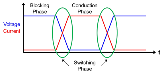 MOSFETs are required to block large voltages between their drain and source during switching.
During the blocking phase the MOSFET must withstand the full rated voltage of the application, while during the conduction and switching phases, losses and switching frequency are important. Conduction and switching losses both impact overall efficiency while higher switching frequencies enable smaller and lighter systems, a key attribute in both EVs and industrial applications.
The trend towards higher voltage is pushing the limits of the traditional silicon MOSFET. However, it is harder and costlier to get the low RDS(on) and high gate charge values required for reduced conduction losses and fast switching times. Power electronics designers are consequently turning to silicon carbide (SiC) to achieve higher efficiencies. SiC, a wide bandgap technology, has several advantages over silicon, including high thermal conductivity, a low thermal expansion coefficient, and high maximum current density, giving it excellent electrical conductivity compared to silicon. Additionally, SiC’s higher critical breakdown field means that a reduced thickness device can support a given voltage rating, leading to significant size reduction.
SiC MOSFETs are now available which can withstand voltage thresholds up to almost 10 kV, compared with 1500 V for the silicon variants. Also, the low switching losses and high operating frequencies of SiC devices enable them to achieve superior efficiencies, particularly in higher-power applications requiring high current, high temperatures, and high thermal conductivity.
onsemi Addresses the Need for Higher VoltagesIn response to the growing demand for devices with high breakdown voltages, onsemi has built an end-to-end in-house SiC manufacturing capability including a range of products such as SiC diodes, SiC MOSFETs, and SiC modules.
This product family includes the NTBG028N170M1, a high-breakdown voltage SiC MOSFET, figure 3. This N-channel, planar device is optimized for fast switching applications at high voltages, with a VDSS of 1700 V, and an extended VGS of ‑15/+25 V.
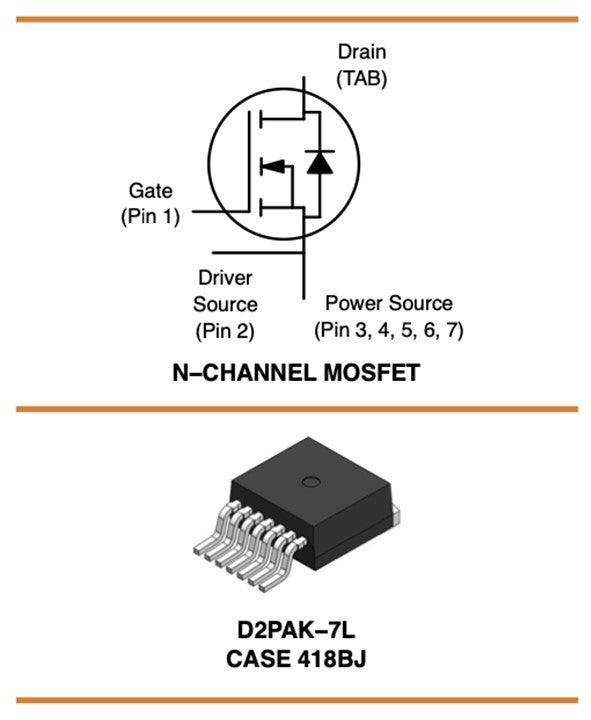 onsemi’s NTBG028N170M1
The NTBG028N170M1 supports drain currents (ID) up to 71 A continuously and 195 A when pulsed and its superior RDS(ON) – typical value 28 mW – mitigates conduction losses. The ultra-low gate charge (QG(tot)), at just 222 nC, ensures low losses during high-frequency operation and the device is housed in a surface mountable D2PAK–7L package, which reduces parasitic effects during operation.
The onsemi EliteSiC range also includes a range of 1700 V-rated SiC Schottky diodes, which complement MOSFETs in power electronics systems such as rectifiers. The high Maximum Repetitive Peak Reverse Voltage (VRRM) of these diodes, along with their low Peak Forward voltage, (VFM) and excellent reverse leakage currents, equip design engineers to achieve stable, high voltage operation at elevated temperatures.
EliteSiC Supports Efficient Power Electronics DesignsThe quest for efficiency is relentless in applications which depend on power electronics devices. The trend towards higher system voltages is challenging the traditional Si-MOSFET and SiC devices offer a way forward, enhancing efficiencies while reducing form factors. The 1700 V NTBG028N170M1 from onsemi enables higher voltage designs for key power electronics systems.
The post Meeting the Demand for Higher Voltage Power Electronics appeared first on ELE Times.
Pages

