
ELE Times

Safely connect & disconnect high current loads to the battery
The Vishay 48V 100A eFuse safeguards power hardware with an adjustable current limit. It securely connects/ disconnects a 48V power source (like a high-energy battery) to any vehicle load by employing Automotive Grade MOSFETs as primary switches, capable of continuous operation up to 100A.
To Download the Whitepaper Please Fill in the Form. >>>>
[contact-form-7]
The post Safely connect & disconnect high current loads to the battery appeared first on ELE Times.
STMicroelectronics boosts sensing creativity with new all-in-one MEMS Studio desktop software solution
Easy to use, efficient, and consolidated tool supports application development for next-gen high-tech MEMS sensor products
STMicroelectronics’ MEMS Studio is a new all-in-one tool for MEMS sensor evaluation and development, connected closely with the STM32 microcontroller ecosystem and available for Windows, MacOS, and Linux operating systems.
By unifying the sensor-development workflow, from evaluation to configuration and programming, MEMS Studio accelerates development and simplifies bringing rich contextual awareness to users’ projects. Enhanced features help easily acquire and clearly visualize sensor data to explore the operating modes and optimize performance and accuracy. There are also tools for pre-built library testing, as well as convenient drag-and-drop algorithm creation for intuitive, no-code development of STM32 MCU firmware.
MEMS Studio supports the wide portfolio of ST MEMS sensors, including motion sensors, environmental sensors, and infrared sensors. It provides tools to explore and use all the sensors’ features including the finite state machine (FSM) and embedded edge AI in inertial modules for power-efficient inferencing directly in the sensor. These include creating and managing decision trees in sensors equipped with ST’s machine-learning core (MLC), monitoring interrupts status, and testing advanced features like FIFO, pedometer, and freefall detection embedded in the sensor.
MEMS Studio also offers a new experience for analyzing sensor data in runtime and offline, where users can visualize, label, and edit the data for the best algorithm implementation. Spectrogram analysis and fast Fourier transform (FFT) are also available and help understand the sensor signal for the best detection of the sensing application target.
Users can choose from a wide variety of compatible development boards, including STM32 Nucleo expansion boards, sensor adapters, and ST’s multi-sensor evaluation kits. These comprise the SensorTile.box PRO, STWIN.box, and STEVAL-MKI109V3 professional MEMS adapter motherboard with adjustable power settings and a STM32F401VE MCU on-board.
As creative use of MEMS sensors continues to drive innovation in cutting-edge applications, MEMS Studio empowers designers to add new and more advanced functions in next-generation high-tech products. Its release promotes the development of smart appliances, medical wearables, and technology for digital healthcare, smart buildings and factories, robotics, asset tracking, and smart driving.
Consolidating and extending the features of established sensor-development tools including AlgoBuilder, Unico-GUI, and Unicleo-GUI, MEMS Studio is available now to download, free of charge, from www.st.com/mems-studio.
STM32 is a registered and/or unregistered trademark of STMicroelectronics International NV or its affiliates in the EU and/or elsewhere. In particular, STM32 is registered in the US Patent and Trademark Office.
The post STMicroelectronics boosts sensing creativity with new all-in-one MEMS Studio desktop software solution appeared first on ELE Times.
Nuvoton Technology for Green Energy, Endpoint AI, and Automotive Applications at Embedded World 2024
Energy saving and power management systems are the next green generation
Nuvoton will be showing green tech, endpoint AI, and automotive products at Embedded World 2024, booth 3A-418 in Germany. These products provide solutions for energy-saving cooling and ventilation, automotive AI guidance and safety challenges, and AI-based manufacturing and smart home demands.
Ultra-Low-Power USB Type-C PD 3.0 MCU, Hydrogen Sensors, Energy-Saving Solutions
Nuvoton’s NuMicro M2L31 microcontroller, with an Arm Cortex-M23 core featuring 64 to 512 Kbytes of ReRAM (Resistive Random-Access Memory), is an ultra-low-power product designed with a commitment to sustainability and energy efficiency. The M2L31 series not only supports two CAN FD and two USB Type-C PD 3.0 connections but also prioritizes robust security features to safeguard valuable data.
Nuvoton’s reference design for a NuMicro M2L31 MCU-based DC fan system compliant with USB Power Delivery 3.0 includes motor drive capability and a user interface to control the fan and upload or display system information. Highlights include BOM cost savings due to integrated features, simplified PCB layout, and flexible input voltage – together, these energy and resource-saving features not only reduce costs but also help create a greener product.
Nuvoton’s other eco-friendly offerings include the KM1M7AF digital power control microcontroller with security features; a compact high-efficiency, low-vibration industrial 48V fan motor driver (KA44370A); a one-chip AC impedance measurement design for efficiency and safety in battery management systems; and an ultra-low power hydrogen sensor that is ideal for monitoring green energy applications such as hydrogen stations, fuel cells, and hydrogen pipelines.
Automotive HMI and Safety ICs Enable Next-Generation Automotive Applications
In the automotive sector, Nuvoton has an automotive Human Machine Interface (HMI) processing IC based around the Gerda graphic processor series. This HMI IC supports fast booting and attractive 2.5D graphics. Its optimized system cost and external component integration are ideal for low-to-mid-end automotive applications.
For automotive safety and AI driving scenarios, Nuvoton’s Multi-Sensing Bridge IC can aggregate and synchronize data from image, audio, depth sensors, and signal processing ICs. This single-package IC with internal DRAM also has XR/VR/AR and drone applications. In addition, Nuvoton will be showing an automotive battery monitoring IC and pack monitoring IC at Embedded World 2024.
AI Vision Warehousing Solutions and Smart Home Technology ICs
Nuvoton displays two user-trainable AI systems for classifying camera data. The Arm Cortex-M55-based M55M1 Automatic Medicine Classifier uses a hardware-accelerated neural network to identify medicines based on visual input and user training. Based on related technology, the Arm Cortex-A35 MA35D1 Intelligent Warehouse Management System is a visual AI system for identifying different varieties of fruit in warehouses and similar environments. Both these systems support LCDs of appropriate size for the user interface.
For smart home products, Nuvoton presents the NAU83G60 Intelligent Smart Amplifier, which is ideal for consumer audio. The company will also be showing a smart ITO panel solution with touch keys and voice prompt capability. This solution is based on the M258 microcontroller with an Arm Cortex-M23 core and features Nuvoton’s fast LCD development and simulation tool, NuTool-LCDView.
The post Nuvoton Technology for Green Energy, Endpoint AI, and Automotive Applications at Embedded World 2024 appeared first on ELE Times.
Rohde & Schwarz first to show measurements on novel Bluetooth Channel Sounding signals for positioning accuracy
Rohde & Schwarz will present the first real-time measurements on the planned new Bluetooth signals to support Channel Sounding. The demonstration at the embedded world Exhibition & Conference in Nuremberg, Germany, will be run on an R&S CMW500 wideband radio communication tester. The Bluetooth Channel Sounding feature will enable unprecedented positioning accuracy for consumer and commercial applications. The signal measurement capabilities to support chip and device development are eagerly awaited by the industry.
For consumer and commercial devices, Bluetooth is the most widely installed technology with location-determining capabilities. Channel Sounding, soon to be introduced, will significantly improve the accuracy of real-time location services for determining position using Bluetooth to an accuracy of 50 cm or better. In addition to improved location accuracy, Channel Sounding is expected to consume less power than existing Bluetooth location services and provide increased security. The improved accuracy will be a major step forward in particular for indoor applications such as asset tracking on the factory floor or in the warehouse, as well as for secure access to buildings or vehicles.
Hardware changes for Bluetooth devices introduced on a new physical layer are required to support the improved location functions. Engineers who want to start developing the necessary chips and devices, including support for Channel Sounding urgently require reliable and accurate measurements on the signals that enable the new functions. Rohde & Schwarz has already prepared options for its R&S CMW platform to support the corresponding RF physical layer measurements.
The current draft of the next version of the Bluetooth Core Specification defines support for phase-based ranging (PBR) tone exchange and round-trip time (RTT). To give hardware and software engineers involved in Bluetooth chipset and device development an early preview of the PBR measurement techniques, Rohde & Schwarz will be presenting a session at the embedded world Conference called “Redefining Bluetooth Low Energy Testing to Cover Latest Bluetooth Innovations” at 1:45 p.m. on April 10. A live demonstration of the measurements will take place at the Rohde & Schwarz booth 4-218 in hall 4 at the embedded world Exhibition in Nuremberg, Germany, April 9 to 11, 2024.
The post Rohde & Schwarz first to show measurements on novel Bluetooth Channel Sounding signals for positioning accuracy appeared first on ELE Times.
Vishay Intertechnology FRED Pt 500 A Ultrafast Soft Recovery Diode Modules in the New TO-244 Gen III Package Deliver High Reliability
Featuring a Common Cathode Configuration, Devices Can Withstand IOL Cycles Up to 5x That of the Previous TO-244 Generation for Improved Life Expectancy While
Reducing Losses
Vishay Intertechnology, Inc. has introduced two new FRED Pt 500 A Ultrafast soft recovery diode modules in the new TO-244 Gen III package. Offering higher reliability than previous-generation solutions, the Vishay Semiconductors VS-VSUD505CW60 and VS-VSUD510CW60 are designed to reduce losses and EMI / RFI in high-frequency power conditioning systems.
The rugged TO-244 package of the diode modules released today withstands 46 000 IOL cycles at given conditions, offering an improved life expectancy over previous-generation devices. In addition, the industry-standard package is footprint-compatible with competing solutions in the TO-244 to provide a drop-in replacement for existing designs.
The VS-VSUD505CW60 and VS-VSUD510CW60 are ideally suited for high-frequency welding; high current converters and ballast water management systems (BWMS) in railway equipment, cranes, and ships; UPS; and other applications where switching losses comprise a significant portion of the total losses. In these applications, the softness of their recovery eliminates the need for a snubber, reducing component counts and lowering costs.
Offered in a common cathode configuration, the diode modules provide low forward voltage drop down to 0.82 V, thermal resistance — junction to case — of 0.16 °C/W, and an operating temperature range up to +175 °C.
Device Specification Table:
| Part number | VS-VSUD505CW60 | VS-VSUD510CW60 |
| VR (V) |
600 |
|
| IF(AV)(A) |
500 |
|
| Qrr typical (nC) | 460 | 1770 |
| trr (ns) | 178 | 270 |
| VFM @ 250 A, +175 °C (V) | 0.95 | 0.82 |
| RthJC per diode (°C/W) |
0.160 |
|
| Package |
TO-244 |
|
The post Vishay Intertechnology FRED Pt 500 A Ultrafast Soft Recovery Diode Modules in the New TO-244 Gen III Package Deliver High Reliability appeared first on ELE Times.
Infineon introduces 80 V MOSFET OptiMOS 7 with lowest on-resistance in the industry for automotive applications
Infineon Technologies AG has introduced the first product in its new advanced power MOSFET technology OptiMOS 7 80 V: The IAUCN08S7N013 features a significantly increased power density and is available in the versatile, robust, and high-current SSO8 5 x 6 mm² SMD package. The OptiMOS 7 80 V offering is a perfect match for the upcoming 48 V board net applications. It is designed specifically for the high performance, high quality and robustness needed for demanding automotive applications like automotive DC-DC converters in EVs, 48 V motor control, for instance, electric power steering (EPS), 48 V battery switches and electric two- and three-wheelers.
Compared to the previous generation, the RDS(on) of the Infineon IAUCN08S7N013 has been reduced by more than 50 per cent and is now the best RDS(on) in the industry with a maximum of 1.3 mΩ. Users benefit from minimized conduction losses, superior switching performance and the highest power density in a 5 x 6 mm² package. In addition, the IAUCN08S7N013 also features low package resistance and inductance, as well as a high avalanche current capability. For automotive applications, it has an extended qualification that goes beyond AEC-Q101.
The post Infineon introduces 80 V MOSFET OptiMOS 7 with lowest on-resistance in the industry for automotive applications appeared first on ELE Times.
Anritsu and the University of Texas at Dallas Collaborate to Showcase Orchestration System for OpenROADM/IPoDWDM at OFC 2024
Anritsu Corporation in collaboration with the University of Texas at Dallas showcased its orchestration system for overall control and monitoring of combined OpenROADM[*1] and IPoDWDM[*2] networks at the Optical Fiber Communication Conference and Exhibition 2024 (OFC2024) on March 26-28, 2024, in San Diego, USA.
These networks are controlled by the YANG model devised by OpenROADM and IETF[*3] as a vendor-independent network control method with an orchestration system managed by the University of Texas at Dallas. In the demonstration, Anritsu’s compact, high-performance MT1040A 400G Tester is connected via an open interface to the Add/Drop line to monitor quality in a live traffic environment.
Today’s network functions are becoming more sophisticated and virtualized for diversifying all-photonics networks and Beyond 5G/6G use cases. Operators expect optimized QoS and reduced maintenance and management costs with automated network settings as well as autonomous operation. Achieving these goals demands integrated transmission and IP network management as well as network quality monitoring.
In this exhibit, two 400G ports on Anritsu MT1040A with built-in 400G OpenZR+ transceivers connected via the Add/Drop line are positioned at each end of an Open ROADM system. In addition to making the channel settings from the orchestration system, the system also monitors line quality data from the MT1040A, providing a unified single system for monitoring communication channel changes based on quality data and for evaluating ROADM path changes.
OpenLab @ UT Dallas contributes to verifying hardware and software interoperability specified by OpenROADM MSA. The lab issues test labels certifying devices that pass interoperability verification and feeds back these test results to OpenROADM MSA.
As a result of this collaboration with the orchestration system for managing OpenROADM and IPoDWDM, Anritsu is contributing to the development of systems for configuring future automated and autonomous networks.
Product Details Network Master Pro (400G Tester) MT1040AMT1040A is a B5 size 400G handheld tester with excellent expandability and operability. It is a touch panel-operated field measurement instrument equipped with a 9-inch screen that is small enough to carry with a single hand. It supports a range of interfaces from 10M up to 400G.
MU104014B is the test module and has the following futures to test 400ZR/ZR+.
- Powerful hardware with cooling for easy handling 400ZR/ZR+ transceivers
- Flexible Settings for All Network Environments
- Grid, Wavelength, Tx Power setting
- Coherent monitoring (OSNR, SOP, CD, etc.) via OIF CMIS
- Media-side FEC monitoring (PreFEC BER) via OIF CMIS
- 1x 400G, 4x 100G, 2x 100G, 1x 100G client signal
- Flexible Layer-2 to Layer-4 configuration
- History Function Monitoring Live Network
- Auto-save all of results at a minimum of 1 second
- CSV output for detailed analysis and comparison
[*1] OpenROADM
Defines interoperability specifications for optical transmission equipment (ROADM), optical transponders, and pluggable optical components, as well as YANG data model specifications, and specifies interfaces for achieving interconnectivity and interoperability between each functional part of an optical transmission network in a multi-vendor environment.
[*2] IPoDWDM
Abbreviation for IP over DWDM technology carrying IP packets directly using high-speed DWDM (dense wavelength division multiplexing) technology. The IP layer and optical transport layer are integrated by combining a transceiver such as OpenZR+ with optical transport functions with the IP router interface to help cut planned capital investment and operation costs.
[*3] IETF
Abbreviation for the Internet Engineering Task Force technical organization tasked with assuring and improving internet interoperability. Defines YANG Model specifications for communications protocols and routers.
The post Anritsu and the University of Texas at Dallas Collaborate to Showcase Orchestration System for OpenROADM/IPoDWDM at OFC 2024 appeared first on ELE Times.
STSPIN32G4, The 1st motor controller with an integrated MCU solves 2 major challenges
Author: STMicroelectronics
The STSPIN32G4 integrates a three-phase gate driver, an STM32G431, and a power management system under one package to solve major engineering challenges, thus enabling new applications. While ST continues to offer STSPIN motor drivers, we also realized that engineers still face several conundrums. Designers want to run more powerful applications but must also shrink their PCBs and reduce costs. Similarly, applications demand more efficiency, but improving it by a few decimal percentage points remains a struggle. ST engineers thus launched the STSPIN32G4 because no other integrated motor controller offered such a powerful mainstream MCU and such a flexible power management system.
STSPIN32G4 and the first challenge: How to make things more powerful in a smaller design? More power under one roof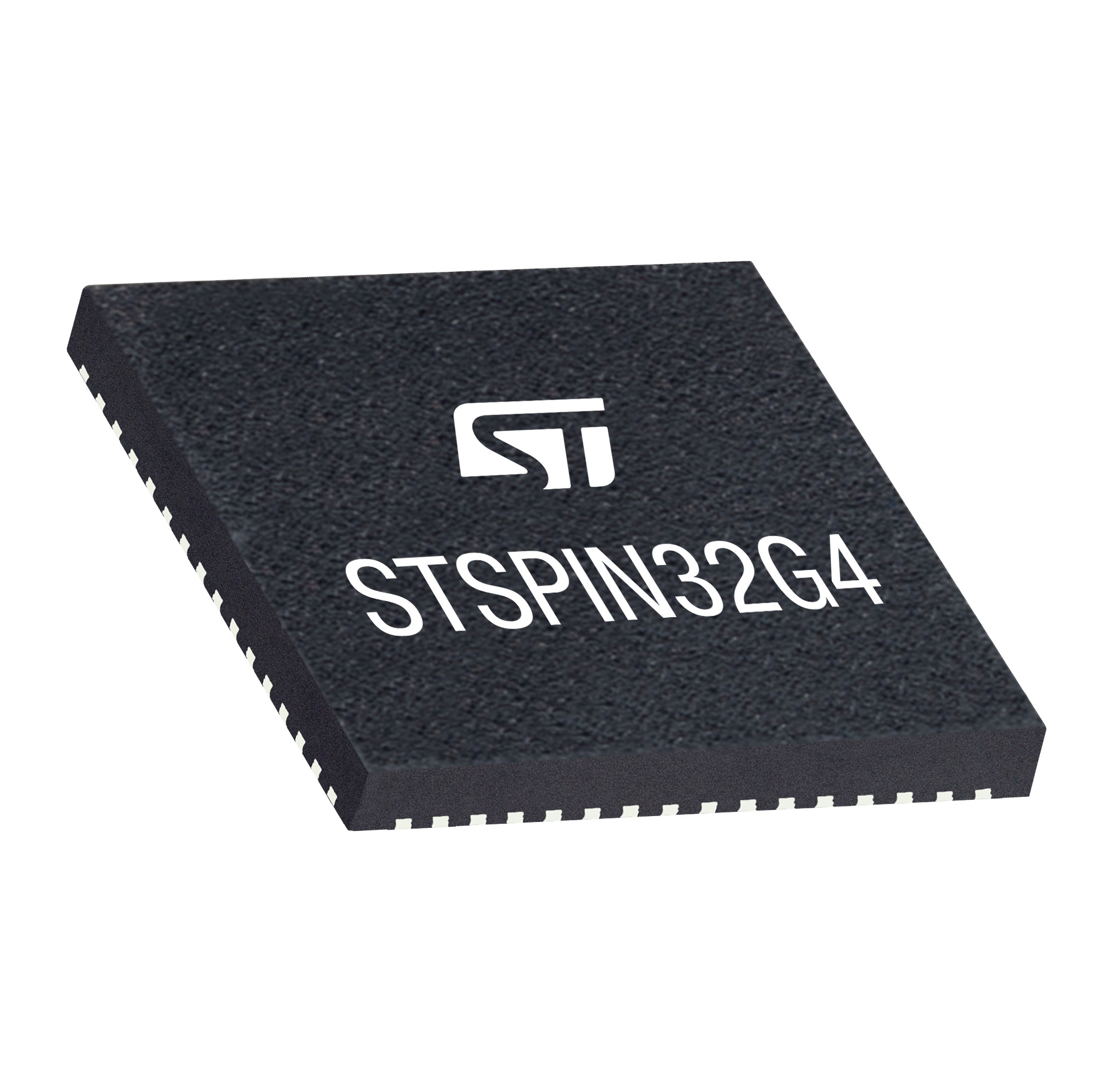 The STSPIN32G4
Let’s take the example of an engineer working on a high-end vacuum cleaner with a high-speed motor. The MCU inside the STSPIN32G4 will stand out, in this instance, because of its computational throughput. A lower-performance CPU core means a lower conversion rate when designing a field-oriented control (FOC) sensorless application. The engineer in the vacuum cleaner example would have to use two or three shunt resistors to compensate for the MCU’s lower performance. On the other hand, the greater computational throughput means a single shunt is sufficient. As a result, using the STSPIN32G4 enables the creation of a powerful application with fewer components.
More peripherals in one deviceA team working on a collaborative robot or a guided vehicle would also appreciate the MCU in the STSPIN32G4 for reasons other than the bump in DMIPS. In this instance, engineers must drive two sets of wheels, but traditional motor controllers don’t have enough analog-to-digital converters to handle such a task. As a result, engineers end up using two motor drivers. The STSPIN32G4 is unique because it provides two sets of PWM timers and 12-bit ADCs, among other things. It, therefore, becomes possible to drive two motors with just one integrated device.
Saving 65% spaceWhile it’s impossible to enumerate all the features in the STSPIN32G4, the reality is that its integrated nature is one of the best ways to solve the space challenge. Motor control applications are increasingly smaller, whether for convenience, costs, or to stand out better. Thanks to its integrated nature, the STSPIN32G4 helps reduce the overall design size by 65% compared to discrete solutions. Practically, it allows engineers to put the control system at the back of the motor and design a much smaller e-bike, vacuum cleaner, or power tool, among other things.
STSPIN32G4 and the second challenge: how to make things more energy efficient while keeping costs down? A more efficient power managementAccording to our benchmarks, using the new device lowers the overall power consumption by 3% to 5% compared to a system that uses external components. A saving of just a single percent already has a significant impact. ST provided such power efficiency by bringing the typical standby consumption to only 15 µA thanks to a very low-quiescent regulator. Hence, we expect engineers to create significantly more compact designs without needing an external cooling system, thus lowering the BoM.
The motor controller also supports a supply voltage of up to 75 V, compared to only 48 V previously. Additionally, the STSPIN32G4 comes with an over-current protection mechanism and a drain-source voltage (VDS) monitoring system that acts as a redundancy. It monitors the external MOSFETs and turns all gate driver outputs off if it detects an over-voltage condition. As a result, we expect engineers to use the STSPIN32G4 in appliances. Indeed, a white good connected to a grid often suffers from wide voltage variations from the mains. The greater supply voltage range and protection features of the new device will better handle these abnormal conditions.
A more flexible power managementEngineers sometimes shy away from integrated solutions, fearing they may restrict their optimization capabilities. Hence, ST ensured a high level of customization. For instance, developers can program registers through an I2C interface to use the STSPIN32G4’s VCC buck converter. Moreover, we published an application note showing how to use the buck regulator in a buck-boost configuration by adding a few external components. Finally, engineers can bypass the buck and LDO regulators to rely on only an external Vcc supply.
Teams that designed a highly precise power supply to meet the stringent requirements of their application can, thus, ignore the STSPIN32G4 regulators. In contrast, others can simplify their designs by using its VCC buck converter to power a few external components, like a memory module. Similarly, developers can choose to enable or disable the standby mode. Such a feature is vital for products like power tools. When users pick a drill after months or even years, they must use it immediately. In such a case, engineers will want to completely disconnect their system from the battery to maximize its usage.
Engineers also get a lot more flexibility in how they drive a motor. They could use a 6-step driver circuit or a field-oriented control, both with or without a sensor and with one, two, or even three shunts. It gives developers the ability to control how much measurement data they gather. Consequently, it also becomes possible to qualify an STSPIN32G4 and use it in many different applications, which can help a company shorten its time to market and optimize its operations.
How to get started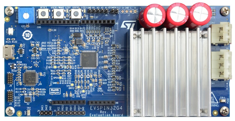 The EVSPIN32G4
ST launched two development boards to enable teams to test and experiment with the STSPIN32G4. The EVSPIN32G4 uses STL110N10F7 power MOSFETs and a heat sink to allow an output current of up to 20 A RMS. As a result, teams can push the new devices to develop more powerful designs. However, ST is also mindful that not every designer will use the STSPIN32G4 in high-powered systems. Hence, we are also launching the EVSPIN32G4NH, a similar development board without passive cooling; NH at the end of the nomenclature stands for “no heat sink”. We also updated the X-CUBE-MCSDK to support the new boards and devices.
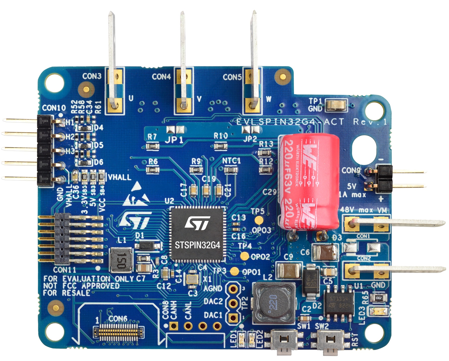 The EVLSPIN32G4-ACT
More recently, our teams released two reference designs. The EVLSPIN32G4-ACT drives a three-phase brushless motor supporting up to 5 ARMS and can manage a supply input of 48 V for a surprising 250 W total power in a board measuring only 62 mm x 50 mm. Additionally, it can connect to the STWIN.box (STEVAL-STWINBX1) to rapidly create a high-speed data logger. Thanks to our FP-IND-DATALOGMC software pack and Quick Start Guide, engineers have a step-by-step process to connect both boards and run applications that can gather data from the sensors on the STWIN.box and the motor itself. We even offer a GUI to help visualize the information.
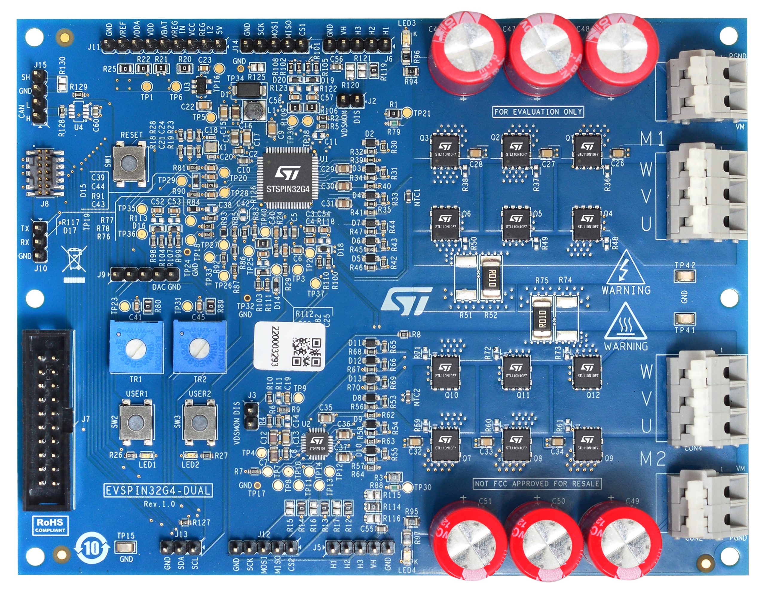 The EVSPIN32G4-DUAL
The other board is the EVSPIN32G4-DUAL, which combines the STSPIN32G4 and the STDRIVE101, a triple half-bridge gate driver. As a result, the board can drive two three-phase brushless motors for up to 10 ARMS output current and a supply of 74 V thanks to two power stages. Thanks to the operational amplifiers of the STSPIN32G4, it’s possible to have a sensor-less system with a single shunt current sensing or use Hall sensors and encoders with the embedded MCU. Put simply, the reference design shows how to create a powerful dual motor application in a small factor for home appliances, e-mobility, pumps, tools, and more.
The post STSPIN32G4, The 1st motor controller with an integrated MCU solves 2 major challenges appeared first on ELE Times.
Anritsu and NTT Collaborate to Showcase End-to-End 400G Testing for IOWN Open APN at OFC2024
Anritsu Corporation, in collaboration with NTT, will participate in the “OFCnet” state-of-the-art network demonstration environment at the Optical Fiber Communication Conference and Exhibition 2024 (OFC2024) to be held in San Diego, USA, from March 26 to March 28, 2024. We will showcase 400G Testing that supports IOWN Open APN[*1].
The demand for interconnection bandwidth between data centres has greatly increased due to the rapid spread of generative AI and cloud services, as well as advances in DX (Digital Transformation). To realize a Datacenter Exchange (DCX) that connects remotely distributed data centres while featuring ultra-high capacity, ultra-low latency, and ultra-low power consumption, the IOWN Global Forum has proposed the Open All-Photonic Network (Open APN) as a new network infrastructure.
At our exhibition, the IOWN Networking Hub (Booth 912), an interconnected booth utilizing OFCnet, will showcase an example Datacenter Exchange (DCX) based on the IOWN APN in a multi-vendor configuration. 400G optical transceivers compliant with the OpenZR+[*2] MSA will be mounted on data centre switches, being interconnected through an OpenROADM network constructed in an adjacent booth, in accordance with OpenROADM MSA[*3] and OpenLab@ University of Texas at Dallas (UTD). Anritsu will provide two interconnected compact and lightweight handheld measuring instruments, MT1040A, that will simultaneously transmit and receive high-bandwidth 400-Gbps traffic, thereby demonstrating the end-to-end performance of the multi-vendor network. The MT1040A flexibly supports standard protocols such as 400G Ethernet, OpenZR+, OpenROADM, and more. It provides real-time measurements of the physical layer (Layer 1) Pre/Post FEC BER, as well as Ethernet (Layer 2) latency and throughput.
Through this collaboration, Anritsu will contribute to forums such as the IOWN Global Forum, Open ROADM, and OpenZR+, with the realization of a data center exchange (DCX) based on the IOWN Open APN architecture. In addition, we will contribute to the construction of automated systems used for orchestration that integrate higher-level network management.
Product Details MT1040A Network Master Pro / MU104014B 400G (QSFP-DD) multi-rate moduleMT1040A is a B5 size 400G handheld tester with excellent expandability and operability. It is a touch panel-operated field measurement instrument equipped with a 9-inch screen that is small enough to carry with a single hand. It supports a range of interfaces from 10M up to 400G.
MU104014B is the test module and has the following futures to test 400ZR/ZR+
- Powerful hardware for easy handling 400ZR/ZR+ transceivers
- Flexible Settings for All Network Environments
- Grid, Wavelength, Tx Power setting
- Coherent monitoring (OSNR, SOP, CD, etc.) via OIF CMIS
- Media-side FEC monitoring (PreFEC BER) via OIF CMIS
- 1x 400G, 4x 100G, 2x 100G, 1x 100G client signal
- Flexible Layer-2 to Layer-4 configuration
- History Function Monitoring Live Network
- Auto-save all of the results at a minimum of 1 second
- CSV output for detailed analysis and comparison
*1 Open APN
Abbreviation for Open All-Photonic Network – an open architecture proposed by the IOWN Global Forum (IOWN GF). It features low power consumption, high capacity, and low latency by configuring an entire section with a photonic network.
*2 OpenZR+
A transceiver interface standard is used mainly in data centre interconnect (DCI). It supports data rates of 100G, 200G, 300G, and 400G, and supports large-scale links of over 120 km with OFEC (forward error correction). Facilitates lower-cost connections between data centres than conventional wavelength division multiplexing (WDM) systems.
*3 OpenROADM MSA
Abbreviation for OpenROADM Multi-Source Agreement, the international organization established to promote OpenROADM.
OpenROADM specifies interconnection specifications for optical transmission equipment (ROADM), optical transponders, and detachable optical components, as well as YANG data model specifications, and defines interfaces for realizing interconnection and interoperability between each functional part of an optical transmission network in a multi-vendor environment.
The post Anritsu and NTT Collaborate to Showcase End-to-End 400G Testing for IOWN Open APN at OFC2024 appeared first on ELE Times.
Renesas Introduces Industry’s First General-Purpose 32-bit RISC-V MCUs with Internally Developed CPU Core
- CPU: RISC-V core at 48MHz, 3.27 Coremark/MHz
- Memory: 128KB code flash, 16KB SRAM (12KB and ECC SRAM 4KB) and 4KB data flash
- Power Consumption: 162µA/MHz (Active power), 0.3µA (SW Standby), 4µs (Standby wakeup)
- Serial communications interfaces: UART, SPI, I2C, SAU
- Analog peripherals: 12-bit ADC and 8-bit DAC
- Temperature range: -40°C to 125°C (Ta)
- Operating voltage range: 1.6 to 5.5V
- Packages: 16 WLCSP, 24/32/48 QFN package (QFP option)
The post Renesas Introduces Industry’s First General-Purpose 32-bit RISC-V MCUs with Internally Developed CPU Core appeared first on ELE Times.
Accelerating the Adoption of AI Applications, Nuvoton Technology Introduces an Endpoint AI Product Platform Based on Microcontrollers and Microprocessors
Nuvoton Technology introduces an endpoint AI platform based on microcontrollers, expanding the AI ecosystem into the microcontroller domain. This solution is based on Nuvoton’s newly designed microcontrollers and microprocessors, including the NuMicro MA35D1, NuMicro M467, and the NuMicro M55M1 series equipped with Arm Ethos-U55 NPU. Nuvoton provides a complete software stack and development tools to facilitate the rapid deployment of advanced machine learning and deep learning models, leveraging advantages such as low power consumption and cost-effectiveness to accelerate the adoption of AI applications, enhancing productivity, and improving human life.
As a leading microcontroller platform provider, Nuvoton not only offers advanced hardware chips but also provides developers with complete software development tools, significantly improving development efficiency. NuEdgeWise is an easy-to-use graphical Python machine learning development tool that provides rich machine learning sample code covering processes such as data collection, labeling, model training, and validation, making the machine learning development process easier.
Nuvoton’s latest microcontroller endpoint AI platform is designed to elevate a wide array of applications, including smart home, security access control, smart city, industrial automation, smart agriculture, interactive toys, fitness equipment, and wearable devices, by infusing embedded system products with advanced AI capabilities.
Endpoint AI microcontroller with Ethos-U55 NPU: NuMicro M55M1
The new NuMicro M55M1 series microcontroller is an innovative Endpoint AI solution that integrates comprehensive microcontroller features, including control, connectivity, security, and advanced machine learning inference capabilities. The M55M1 microcontroller features a 200 MHz Arm Cortex-M55 CPU and a 200 MHz Arm Ethos-U55 NPU, providing machine learning inference capability and supporting CNN and RNN operations. It includes built-in 1.5 MB SRAM and 2 MB flash memory and can expand HYPERRAM or HYPERFLASH via the HYPERBUS interface. To enhance the overall performance of application systems, the M55M1 microcontroller incorporates three unique features to optimize system performance, security, and power consumption. Firstly, it enables continuous operation of image sensors, microphones, and various sensors in a low-power sleep mode, allowing for constant monitoring of predefined events such as personnel presence or significant sound and vibration detection. Secondly, it stores machine learning model data in an area accessible only to the NPU but not to the CPU, to prevent malicious programs from stealing model data and thus protect intellectual property. Lastly, the M55M1 also implements sine and cosine hardware circuits, which are defined within Arm’s custom instructions for easy invocation by software. These unique features of M55M1 empower developers to develop endpoint AI applications that achieve performance, power efficiency, and security.
High-performance edge industrial IoT series: NuMicro MA35D1
The NuMicro MA35D1 series heterogeneous multicore microprocessor is designed to meet the high-end industrial IoT requirements, featuring dual-core Arm Cortex-A35 64-bit processors with a maximum frequency of 800 MHz and a 180 MHz Arm Cortex-M4F core. Combined with a USB camera and CNN models, MA35D1 can perform endpoint AI tasks such as object detection.
The Ethernet/Crypto MCU with excellent security and connectivity: NuMicro M467
The M467 series features a 200 MHz Arm Cortex-M4F core with a built-in DSP instruction set and a single-precision floating-point unit (FPU). With the tinyML software technology, the M467 can perform various endpoint AI applications, such as gesture recognition, equipment anomaly detection, and keyword spotting. The M467 series microcontrollers have also participated in the MLPerf Tiny Benchmark test, demonstrating excellent inference speed across four endpoint AI tasks.
Complete machine learning development tools – Accelerating the implementation of AI applications
In addition to innovative microcontroller specifications, Nuvoton also supports a complete machine-learning software development stack for developers to develop machine-learning applications. The software stack includes NuEdgeWise Python development environment and machine learning sample code, Tensorflow machine learning model training framework, Vela neural network compiler dedicated to Ethos NPU, Tensorflow Lite for microcontroller inference framework, Arm CMSIS-NN machine learning library, and Ethos-U55 NPU driver.
Nuvoton’s endpoint AI microcontrollers enhance products across a diverse range of applications – including smart home, security access control, smart city, industrial automation, smart agriculture, interactive toys, fitness equipment, and wearable devices – by seamlessly integrating AI capabilities to deliver added value.
The post Accelerating the Adoption of AI Applications, Nuvoton Technology Introduces an Endpoint AI Product Platform Based on Microcontrollers and Microprocessors appeared first on ELE Times.
Microchip Technology Expands TrustFLEX Family with CEC1736 Real-time Platform Root of Trust Devices
TrustFLEX devices along with the Trust Platform Design Suite tool will simplify the enablement of the root of trust from concept to production in a wide range of applications
As technology and cybersecurity standards continue to evolve, Microchip Technology is helping make embedded security solutions more accessible with its CEC1736 TrustFLEX devices. The CEC1736 Trust Shield family is a microcontroller-based platform root of trust solution enabling cyber resiliency for data centres, telecom, networking, embedded computing and industrial applications. Now, as part of the TrustFLEX platform, the devices are partially configured and provisioned with Microchip-signed Soteria-G3 firmware to reduce the development time needed to integrate the platform root of trust. These devices also help fast-track the provisioning of required cryptographic assets and signed firmware images, simplifying the process of secure manufacturing as required by the National Institute of Standards and Technology (NIST) and Open Compute Project (OCP) standards.
Specifically designed to meet NIST 800-193 platform resiliency guidelines, as well as OCP requirements, CEC1736 TrustFLEX devices can support security features necessary to enable hardware root of trust across various markets. The Trust Platform Design Suite tool will allow customers to personalize platform-specific configuration settings, including unique credentials, to support any application, host processor or SoC that boots out of an external SPI Flash device to extend the root of trust in the system.
“Microchip has led our industry in streamlining secure provisioning from design to deployment for devices and platforms of all scales. This rich range of solutions now include OCP-compliant root of trust devices,” said Nuri Dagdeviren, corporate vice president of Microchip’s secure computing group. “With the pre-configured CEC1736 TrustFLEX family, we are helping lower the barrier of entry and making it easier for customers to implement platform root of trust and enable faster prototyping and speed to market.”
Modern firmware security features enabled on the CEC1736 TrustFLEX—like SPI bus monitoring, secure boot, component attestation and lifecycle management—can keep both the pre-boot and real-time (time of check and time of use) environments shielded from both in-person and remote threats.
The highly configurable, mixed-signal, advanced I/O CEC1736 controllers integrate a 32-bit 96 MHz Arm Cortex-M4 processor core with closely coupled memory to offer optimal code execution and data access.
The post Microchip Technology Expands TrustFLEX Family with CEC1736 Real-time Platform Root of Trust Devices appeared first on ELE Times.
Vertiv Joins the NVIDIA Partner Network
Vertiv brings its high-density power and cooling infrastructure expertise to the NVIDIA Partner Network to better support adoption of accelerated computing and AI workloads
Vertiv, a global leader in critical infrastructure and continuity solutions, is now a Solution Advisor:Consultant partner in the NVIDIA Partner Network (NPN), providing wider access to Vertiv’s experience and a full portfolio of power and cooling solutions.
NPN is a global program for technology partners who offer solutions built on or powered by NVIDIA technologies. Among leading software vendors, cloud service providers, solution providers, and system integrators, Vertiv joins the network to offer its expertise in addressing the unique infrastructure challenges presented by accelerated computing. NPN provides access to a range of benefits, including technical support, training, and collaboration opportunities, helping partners deliver innovative solutions to their customers.
“Vertiv has collaborated with NVIDIA in research, development, and engineering for multiple years, designing innovative products and solutions that support the deployment of NVIDIA technologies globally,” said Giordano (Gio) Albertazzi, CEO at Vertiv. “We have combined our leadership in power and cooling solutions with NVIDIA’s cutting-edge platforms to help meet the demands of the most compute-intensive applications and support the deployment of AI infrastructure across the globe. Now, we are collaborating to build state-of-the-art liquid cooling solutions for next-gen NVIDIA accelerated data centers powered by GB200 NVL72 systems.”
Vertiv’s high-density power and cooling solutions are designed to support the next generation of GPUs running the most compute-intensive AI workloads safely, at optimal performance and with high availability. Vertiv’s portfolio of liquid cooling technologies, such as Vertiv Liebert XDU coolant distribution units, Vertiv Liebert XDM split indoor chillers, and Vertiv Liebert DCD rear-door heat exchangers, cover a wide range of application requirements. The Vertiv Geist rack power distribution units (PDUs) family has been extended to accommodate higher power draw within the rack, minimizing footprint while maintaining high efficiency.
The post Vertiv Joins the NVIDIA Partner Network appeared first on ELE Times.
New SSO10T TSC top-side cooling package for power MOSFETs enables highest efficiency for modern automotive applications
Infineon Technologies AG introduces the SSO10T TSC package with OptiMOS MOSFET technology. With its direct top-side cooling concept, the package offers excellent thermal performance. This eliminates heat transfer into or through the PCB of the automotive electronic control unit. The package enables a simple and compact double-sided PCB design and minimizes cooling requirements and system costs for future automotive power designs. The SSO10T TSC is therefore well suited for applications such as electric power steering (EPS), EMB, power distribution, brushless DC drives (BLDC), safety switches, reverse battery, and DCDC converters.
The SSO10T TSC has a 5 x 7 mm² footprint and is based on the established industry standard SSO8, a 5 x 6 mm² robust housing. However, due to its top-side cooling, the SSO10 TSC offers more than 20 percent and up to 50 percent higher performance than the standard SSO8 – depending on the thermal interface (TIM) material used and the TIM thickness. The SSO10T TSC package is JEDEC listed for open market and provides wide second source compatibility. As a result, the package can be introduced quickly and easily as the future standard for top-side cooling.
The SSO10T package enables a very compact PCB design and reduces the system footprint. It also lowers the cost of the cooling design by eliminating vias, resulting in lower overall system costs and design effort. At the same time, the housing offers high power density and efficiency, thus supporting the development of future-proof and sustainable vehicles.
AvailabilityThe first 40 V automotive MOSFET products with SSO10T are now available: IAUCN04S6N007T, IAUCN04S6N009T, IAUCN04S6N013T, IAUCN04S6N017T. Further information is available at https://www.infineon.com/cms/en/product/promopages/SSO10T/.
Infineon at Embedded WorldEmbedded World will take place from 9 to 11 April, 2024 in Nuremberg, Germany. Infineon will present its products and solutions for decarbonization and digitalization in hall 4A, booth #138 and virtually. Company representatives will also hold several TechTalks as well as presentations at the accompanying Embedded World Conference, followed by discussions with the speakers. If you are interested in interviewing an expert at the show, please email media.relations@infineon.com. Industry analysts interested in a briefing can email MarketResearch.Relations@infineon.com. Information about the Embedded World show highlights is available at www.infineon.com/embeddedworld.
The post New SSO10T TSC top-side cooling package for power MOSFETs enables highest efficiency for modern automotive applications appeared first on ELE Times.
Infineon extends its XDP digital power protection controller family with the XDP700-002, the industry’s first wide input voltage hot-swap controller for telecom infrastructure
Infineon Technologies AG is expanding its XDP digital power protection controller product family with the XDP700-002, the industry’s first -48 V wide input voltage digital hot-swap controller with a programmable safe operating area (SOA) control designed for telecom infrastructure. It boasts superior current reporting accuracy of less than ±0.7 percent, enhancing the system’s fault detection and reporting accuracy. Furthermore, the product features boost-mode control technology for safer turn-on of field-effect transistors (FETs) in systems with non-optimal SOA. This new member of the XDP product family is tailored for a spectrum of telecom applications, including remote radio head power, base station power distribution, active and passive antenna systems, 5G small cell power, and telecom UPS systems.
The XDP700-002 employs a three-block architecture that combines high-precision telemetry for monitoring and fault detection, digital SOA control optimized for power MOSFETs, and integrated gate drivers for n-channel power MOSFETs. The XDP700-002 operates within an expansive -6.5 to -80 V input voltage range and can withstand transients up to -100 V for 500 ms, delivering current and voltage telemetry with a remarkable 0.7 percent and 0.5 percent accuracy respectively. It features precise PMBus compliant active monitoring for enhanced system reliability. A programmable gate shutdown during severe overcurrent (SOC) ensures robust shutdown operation within just 1 µs. The advanced closed-loop SOA control ensures higher MOSFET reliability, and the fully digital operating mode minimizes the need for external components offering a compact solution making it an optimal fit for space-constrained designes in a cost-effective way.
With options for external FETs selection and a one-time programmable (OTP) option, the XDP700-002 offers flexibility for programming faults and warnings detection as well as de-glitch levels for various usage models. Its analog-assisted digital mode offers backward compatibility with legacy analog hotswap controllers. By offering robust functionality and adaptability, the XDP700-002 exemplifies Infineon’s continuous commitment to innovation and system reliability in telecom infrastructure.
The controller perfectly matches Infineon’s OptiMOS and OptiMOS Linear FET portfolio for reliable and powerful system performance.
Availability
The XDP700-002 hot-swap and system monitoring controller IC is available in a VQFN-29 6×6 package and can be ordered now. More information is available at www.infineon.com/xdp700-002.
The post Infineon extends its XDP digital power protection controller family with the XDP700-002, the industry’s first wide input voltage hot-swap controller for telecom infrastructure appeared first on ELE Times.
Infineon presents innovative semiconductor and microcontroller solutions for a greener future at embedded world 2024
Decarbonization and digitalization are the two central challenges of our time, but they rely on new and advanced technologies. At embedded world 2024 in Nuremberg, Infineon Technologies AG (FSE: IFX / OTCQX: IFNNY) will demonstrate how its innovative semiconductor solutions support and drive these advancements. Microcontrollers in particular play an important role as they are at the heart of a wide range of applications, from electric vehicles and renewable energy systems to smart homes and industrial automation. For this reason, Infineon showcases high-quality microcontrollers designed with the latest technologies and innovative features such as enhanced security and high accuracy, offering excellent performance with low power consumption.
Under the motto “Driving decarbonization and digitalization. Together.” Infineon invites its customers to embedded world 2024 to demonstrate innovative semiconductor solutions that contribute to a more sustainable future. In addition, customers can register for Infineon’s digital platform – the perfect place to dive deeper into the various technologies presented at EW during and after the event. The Infineon booth in Hall 4A (booth #138) will present highlights from the consumer and IoT, automotive, and industrial sectors.
Consumer and IoT: With its broad portfolio of IoT solutions, Infineon supports manufacturers in providing consumers with more comfortable, secure, and energy-efficient homes and buildings by utilizing the company’s latest microcontroller, sensor, security, and connectivity solutions. In this area, visitors will discover:
- Robotics development platform: The platform includes hardware and software solutions for key robotics subsystems such as main and motor controllers, battery management systems and sensors, which enable developers to get robots up and running faster and easier.
- Better sleep quality with XENSIV
 : Leveraging Infineon’s 60 GHz radar, PSoC and Wi-Fi® technologies, the XENSIV Sleep Quality Service is designed to measure and optimize the user’s sleep based on their individual needs.
Simplifying air quality monitoring and optimizing energy efficiency with the new XENSIV PAS CO2 5V kits: The XENSIV PAS CO2 5V Sensor2Go kit provides
- developers with seamless CO2 sensor integration and a plug-and-play solution. The effortless connection to the graphical user interface (GUI) allows users to accurately analyze CO2 data in real time from multiple kits.
- Land a rocket on the Edge: This fun game demonstrates the PSoC Edge device’s ability to integrate multiple functions such as high-performance computing, graphics processing and display, acoustic activity recognition, speech recognition, sensing and gesture recognition with ML in the same chip and application.
Automotive: As a leading supplier of automotive solutions, Infineon focuses on making smart cars a reality with proven microcontroller, connectivity, security, and sensor technologies for the industry. The company’s microelectronics play a critical role in delivering zero-emission vehicles that are smart, connected, safe and reliable.
- AI-based siren recognition: Infineon showcases an autonomous car that recognizes emergency vehicles by their characteristic siren sound and reacts accordingly without violating traffic regulations. This system solution combines MEMS microphones, a microcontroller unit (MCU), and AI software from Imagimob.
- Next generation eMobility: Infineon enables next-generation vehicles with the AURIX TC4x microcontroller family and the AURIX Development Studio (ADS). With these solutions, manufacturers can easily implement modern ADAS, advanced automotive E/E architectures and affordable Artificial Intelligence (AI) applications.
- TRAVEO T2G Cluster 6M Lite Kit: With the TRAVEO T2G CYT4DL device prototypes can be implemented in the shortest possible time and at minimal cost.
Industrial: Infineon supports smart factories and provides manufacturers with a broad sensor portfolio and an extensive partner network. In this way, the company enables reliable data acquisition and processing that enables condition monitoring and predictive maintenance in various Industry 4.0 use cases:
- Predictive maintenance: In this sector, Infineon will present a portable HVAC system equipped with the XENSIV Predictive Maintenance Evaluation Kit. The demo includes a TinyML model and a cloud-based AI service solution generator.
At the Infineon booth, the company has set up a comprehensive series of TechTalks. The seven presentations will cover a wide range of different topics, from software to products, and from consumers to industry. Full details of all Infineon conference presentations, technical workshops and TechTalks can be found here.
Daily program of the Tech Talks- “Ambient sensing: Infineon radar solutions: How Infineon’s tools and enablement can accelerate your time to market” at 10:00 a.m. presented by Firas Labidi
- “Embedded AI and safety – Embedded AI will enable the innovations for next generation of electric vehicle and autonomous driving” at 11:00 a.m. presented by Jürgen Schäfer
- “Accelerate your product development with system reference designs” at 12:00 p.m. presented by Jaya Bindra
- “Addressing the next generation of Edge AI devices with PSoC Edge” at 1:00 p.m. presented by Rebecca Phillips
- “TRAVEO T2G MCUs for automotive HD front lighting” at 2:00 p.m. presented by Maniacherry Devassy Anu
- “Unlocking the power of Edge AI with Imagimob and ModusToolbox” at 3:00 p.m. presented by Alexander Samuelsson
- “Infineon’s solutions for robotics” at 4:00 p.m. presented by Nenad Belancic
Embedded World will take place from 9 to 11 April, 2024 in Nuremberg, Germany. Infineon will present its products and solutions for decarbonization and digitalization in hall 4A, booth #138 and virtually. Company representatives will also hold several TechTalks as well as presentations at the accompanying Embedded World Conference, followed by discussions with the speakers. If you are interested in interviewing an expert at the show, please email media.relations@infineon.com. Industry analysts interested in a briefing can email MarketResearch.Relations@infineon.com. Information about the Embedded World show highlights is available at www.infineon.com/embedded-world.
The post Infineon presents innovative semiconductor and microcontroller solutions for a greener future at embedded world 2024 appeared first on ELE Times.
embedded world 2024: Rohde & Schwarz presents its cutting-edge test solutions for embedded systems
Embedded systems are the foundation of today’s electronic devices, spanning sectors as diverse as consumer electronics, telecommunications, industrial, medical, automotive and aerospace applications. Ensuring seamless operation is critical, which means that engineers encounter complex challenges as they design increasingly compact embedded systems and align them with today’s requirements for efficiency, safety, reliability and interoperability. Rohde & Schwarz offers comprehensive test and measurement solutions to meet these challenges and will present its highlights at the embedded world Exhibition & Conference 2024 in Nuremberg, Germany.
Rohde & Schwarz is showcasing its state-of-the-art test and measurement solutions tailored to the embedded industry at the embedded world Exhibition & Conference. At the company’s booth 4-218 in hall 4 of the Nuremberg Exhibition Center, visitors will have the opportunity to gain insights into embedded design testing, including testing of digital designs and interfaces, power electronics, electromagnetic compatibility, wireless connectivity and in-vehicle networks.
One-box test solution supports new Bluetooth® Low Energy test features
One highlight will be the R&S CMW wideband radio communication test platform (R&S CMW500, R&S CMW270) covering the new Low Energy (LE) feature Bluetooth Channel Sounding (CS). CS extends the positioning capabilities of low energy devices based on high accuracy distance measurements. The R&S CMW platform offers fully featured RFPHY test capabilities using the phase-based ranging (PBR) principle. High-performance internal signal generators and analyzers allow repeatable high-quality device verification.
The R&S CMW platform also supports Bluetooth® Low Energy over-the-air (OTA) receiver and transmitter measurements, as defined in the upcoming Unified Test Protocol (UTP) test mode. The OTA test capability allows easy RFPHY testing of devices that do not have a physical test connector. The new Bluetooth core specification defining the CS and UTP modes is expected to be released later this year.
The R&S CMW platform is a comprehensive, fully automated test solution for verifying the physical layer functions Bluetooth Low Energy and Bluetooth Classic with the addition of LE audio measurements. Visitors can experience the new LE test modes live at the Rohde & Schwarz booth.
Eight-channel MXO 5 oscilloscope sets new signal analysis standardsAnother highlight is the MXO 5 oscilloscope from Rohde & Schwarz, the world’s first eight-channel oscilloscope that can detect 4.5 million acquisitions and a total of 18 million waveforms per second across multiple channels. The MXO 5 shows more of a signal’s activity than any other oscilloscope in both the time and frequency domains. With a simultaneous acquisition memory of 500 Mpoints across all eight channels, it offers twice the standard memory of competitive models. As the first eight-channel oscilloscope with digital triggering, it sets a new standard for signal analysis. It is also the first oscilloscope to offer 45 000 FFTs per second. Visitors to the Rohde & Schwarz booth will have the opportunity to see this innovative instrument in action, testing system-on-chip (SoC) power designs with multiphase buck converters.
Testing signal integrity in high-speed digital designsHigh-speed digital interfaces play a pivotal role in electronic designs. Increasing data rates and integration densities are a challenge for designs at the IC, board and system levels. Visitors to the show can learn about powerful tools for system verification and debug, as well as compliance testing for signal integrity in interfaces, PCBs and interconnects, directly from experts in the field. Demo setups at the Rohde & Schwarz booth include USB 3.2 signal integrity debugging with receiver equalization emulation and advanced eye diagram analysis with the R&S RTP164B oscilloscope, as well as protocol decoding with the MXO 4 oscilloscope.
In addition, visitors will find a solution for fully automated (pre-)compliance testing and verification of high-speed cables (IEEE 802.3bj/by/cd/ck and PCIe 5.0/6.0) using the R&S ZNrun automation test suite, an R&S ZNA or R&S ZNB vector network analyzer and the R&S OSP320 open switch and control platform. The multiport physical layer analysis of a PCIe 6.0 compliant cable is performed by accurately de-embedding the signal with the R&S ZNB43 vector signal analyzer.
R&S CMX500 with new Wi-Fi 7 R&D capabilitiesThe new Wi-Fi 7 standard supports up to 16×16 MIMO with 320 MHz wide channels and 4096 QAM modulation, providing extremely fast and stable connections. When developing Wi-Fi 7 devices, the RF TX and RX characteristics must be measured under real-world conditions in signaling mode. The R&S CMX500 multi-technology multi-channel signaling tester is now available with integrated Wi-Fi 7 test functions. Test environments with multiple RF chains are particularly important in Wi-Fi 7, where multilink operation (MLO) is a key feature. The tester’s flexibility, support for multiple radio technologies and embedded IP test capabilities make it a versatile solution for a wide range of Wi-Fi 7-specific tests, such as 2×2 MIMO, 6 GHz band with out-of-band discovery, coexistence and E2E test capabilities.
Solving test challenges for UWB verification and FiRa Consortium certificationAccurate ranging, low power consumption, high security and reliability – these are the features of ultra-wideband (UWB) technology features that make it suitable for many secure ranging applications, especially as a digital key. At embedded world 2024, Rohde & Schwarz will present the R&S CMP200 radio communication tester with integrated UWB test capabilities for solving UWB test challenges in mass production as well as in R&D.
Analyzing and debugging electromagnetic emissionsBecause all electronic controllers are susceptible to conducted or radiated electromagnetic emissions, many finished electronic products fail their first EMC compliance test. Every day spent debugging, isolating and correcting the EMI problem increases the time to market. As a leader in EMC testing, Rohde & Schwarz will present solutions that integrate EMI testing into the product design process. Visitors can learn how to use the powerful R&S RTO6 oscilloscope for EMI debugging or the R&S FPL1000 signal and spectrum analyzer for EMC pre-compliance testing.
EMC compliance testingRohde & Schwarz offers the R&S ESW EMI test receiver for final EMC compliance tests. With the new R&S ESW-B1000 wideband option, the R&S ESW can expand its FFT bandwidth to up to 970 MHz to measure the complete CISPR frequency Bands C and D in a single operation. The wide bandwidth helps to intercept sporadic interference and enables higher reliability and repeatability in commercial and MIL-STD tests. The extremely high measurement speed opens up new possibilities for compliance testing as well as for emissions analysis and debugging. The R&S EPL1000 EMI test receiver offers fast, accurate and reliable EMI compliance measurements up to 30 MHz at a competitive price in the full CISPR 16-1-1 compliance receiver class for both device developers and conformance test houses.
Battery simulation and power consumption testingBattery life is usually one of the most important specifications for battery-powered devices. Visitors can explore the R&S NGM200 high-precision DC power supply in a battery testing and simulation setup. The application software facilitates battery discharging, as well as the repeated discharge and recharge of rechargeable batteries. Continuous monitoring and recording of open circuit voltage and voltage under load are integral features. The DC power supply can be remotely controlled from a PC with the application software installed.
Another test setup allows visitors to use various smartwatch apps to observe how GPS affects power consumption in real time. A new analysis tool helps developers analyze power consumption data collected with the R&S NGU power supply. These source measure units can be used for battery modeling and simulation. They measure the current consumption of battery-powered devices in all phases and during the transition from sleep to active mode, which is important for design engineers.
Component testing: high speed VCO tester and an LCR meter with sweep softwareRohde & Schwarz will present its R&S FSPN high-speed phase noise analyzer up to 50 GHz in a demonstration test setup with a VCO device under test. Equipped with two low phase noise synthesizers and a real-time cross-correlation engine for increased measurement sensitivity, it is ideal for characterizing sensitive synthesizers and oscillators in R&D. In addition, Rohde & Schwarz will showcase its R&S LCX200 LCR meters with customized impedance measurement functions that are suitable for all discrete passive components up to 10 MHz. Using the R&S LCX sweep software tool, they can even perform sweep measurements displaying numerous charts. The MFIA impedance analyzer from Zurich Instruments AG (a subsidiary since 2021) will also be on display. The MFIA provides impedance analysis for both low and high impedance components and has a measurement mode for quickly tracking impedance changes in devices under test.
These and other test solutions can be found at the Rohde & Schwarz booth 4-218 in hall 4 at the embedded world Exhibition & Conference from April 9 to 11, 2024 in Nuremberg, Germany. For more information visit: www.rohde-schwarz.com/embedded-world
The post embedded world 2024: Rohde & Schwarz presents its cutting-edge test solutions for embedded systems appeared first on ELE Times.
New Renesas MCUs conserve energy with high-res analog and OTA update support
Low-Power, Streamlined Devices Target Energy Management, Home Appliances, Building Automation and Medical Applications
- Core: 48MHz Arm Cortex-M23
- Memory: 512KB integrated, dual-bank Flash memory and 48KB SRAM
- Analog Peripherals: 24-bit Sigma Delta ADC with digital filter, 12-bit ADC, and temperature sensor.
- Packages: 100-, 80- and 64-pin LFQFP
The post New Renesas MCUs conserve energy with high-res analog and OTA update support appeared first on ELE Times.
Cadence and NVIDIA Unveil Groundbreaking Generative AI and Accelerated Compute-Driven Innovations
Cadence Reality Digital Twin Platform integrated with NVIDIA Omniverse and Orion molecular design platform accelerated with NVIDIA BioNeMo will transform the future of design
Cadence Design Systems, Inc. today announced an expansion of its multi-year collaboration with NVIDIA across EDA, system design and analysis, digital biology and AI with the unveiling of two transformative solutions to reinvent design using accelerated computing and generative AI.
First, the new Cadence Reality Digital Twin Platform is the industry’s pioneering comprehensive digital twin solution to facilitate speed-of-light acceleration of the design, simulation and optimization of data centers across multiple industries. The platform virtualizes the entire data center and uses AI, high-performance computing (HPC) and physics-based simulation to significantly improve data center energy efficiency by up to 30%.
The Cadence Reality platform’s integration with NVIDIA Omniverse brings OpenUSD data interoperability and physically based rendering to the digital twin solution—helping accelerate data center design and simulation workflows by 30X.
Second, the companies are collaborating on generative AI to dramatically accelerate approaches to drug discovery. Cadence’s cloud-native molecular design platform Orion® will now be supercharged with NVIDIA’s generative AI tool, NVIDIA BioNeMo , and NVIDIA microservices for drug discovery to broaden therapeutic design capabilities and shorten time to trusted results. The collaboration brings together decades of expertise in scientific software and accelerated computing from the two companies to deliver transformative approaches to drug discovery. Accelerated by on-demand GPU access at an unprecedented scale, pharmaceutical companies can quickly and reliably generate and assess design hypotheses across a range of therapeutic modalities, including biologics, peptides and small molecules.
“The broadening collaboration between NVIDIA and Cadence is having a transformative impact on everything from data center design to drug discovery,” said Dr. Anirudh Devgan, president and CEO, Cadence. “As AI rapidly becomes a keystone technology driving data center and data center workload expansion, the Cadence Reality Digital Twin Platform integration with NVIDIA Omniverse will optimize every aspect of data center design and operations, use energy more efficiently, and pave the way for a more efficient, resilient, and environmentally friendly future. Our groundbreaking efforts with NVIDIA to integrate BioNeMo with our industry-leading Orion molecular design tools hold great promise for unlocking new ideas and transforming the future of therapeutics and drug discovery. Together, NVIDIA and Cadence are leading the AI revolution.”
“Digital twins will transform manufacturing, drug discovery and countless other industries,” said Jensen Huang, founder and CEO of NVIDIA. “Using NVIDIA Omniverse and generative AI technologies, Cadence can deliver simulation and digitalization technologies to benefit individuals, companie and societies in ways we have yet to imagine.”
Growing Importance of Digital Twin TechnologyDigital twin technology is increasingly becoming critical to designers and operators of complex data center systems in the AI era as through creating a virtual replica of a physical system, it can use real-time data to simulate its behavior, performance and interactions in various conditions. The Cadence Reality platform provides visibility across the entire value chain, enabling data center designers and operators to simulate the performance of integrated liquid and air-cooling systems, visualize the performance of data centers and plan for what-if scenarios.
The company’s collaboration with NVIDIA also expands the capabilities of the Orion drug discovery platform by providing key capabilities, including access to BioNeMo models for structure prediction, small molecule generation and molecular property prediction. Molecules generated with BioNeMo may then be profiled and iteratively enhanced and designed with Orion tools.
Today’s announcements build upon Cadence and NVIDIA’s long-standing collaboration in areas such as:
- AI-driven digital and custom IC design, including PPA, schedule and cost reduction of NVIDIA GPUs with Cadence Innovus and Cadence Cerebrus solutions
- Over 20 years of partnership in hardware and software verification, including Palladium, Protium, and now Cadence Verisium technologies
- System design and analysis, including GPU-optimized Cadence Fidelity CFD Software and the revolutionary Cadence Millennium Enterprise Multiphysics Platform
These announcements also open a new chapter of Cadence’s Intelligent System Design strategy to help customers develop differentiated products across a wide range of industries and market verticals.
The post Cadence and NVIDIA Unveil Groundbreaking Generative AI and Accelerated Compute-Driven Innovations appeared first on ELE Times.
STMicroelectronics Reports on Resolutions to be Proposed at the 2024 Annual General Meeting of Shareholders
STMicroelectronics, a global semiconductor leader serving customers across the spectrum of electronics applications, announced the resolutions to be submitted for adoption at the Annual General Meeting of Shareholders (AGM) which will be held in Amsterdam, the Netherlands, on May 22, 2024.
The resolutions, proposed by the Supervisory Board, are:
• The adoption of the Remuneration Policy for the Supervisory Board;
• The adoption of the Company’s statutory annual accounts for the year ended December 31, 2023, prepared in accordance with International Financial Reporting Standards (IFRS). The 2023 statutory annual accounts were filed with the Netherlands authority for the Financial Markets (AFM) on March 21, 2024 and are posted on the Company’s website (www.st.com) and the AFM’s website (www.afm.nl);
• The distribution of a cash dividend of US$ 0.36 per outstanding share of the Company’s common stock, to be distributed in quarterly installments of US$ 0.09 in each of the second, third and fourth quarters of 2024 and first quarter of 2025 to shareholders of record in the month of each quarterly payment as per the table below;
• The amendment to the Company’s Articles of Association;
• The adoption of the Remuneration Policy for the Managing Board;
• The reappointment of Mr. Jean-Marc Chery as member and Chairman of the Managing Board for a three-year term to expire at the end of the 2027 AGM;
• The approval of the stock-based portion of the compensation of the President and CEO;
• The appointment of Mr. Lorenzo Grandi as member of the Managing Board for a three-year term to expire at the end of the 2027 AGM;
• The approval of the stock-based portion of the compensation of the Chief Financial Officer;
• The approval of a new 3-year Unvested Stock Award Plan for Management and Key Employees;
• The reappointment of EY as external auditor for the 2024 and 2025 financial years;
• The reappointment of Mr. Nicolas Dufourcq, as member of the Supervisory Board, for a three-year term to expire at the end of the 2027 AGM;
• The reappointment of Ms. Janet Davidson, as member of the Supervisory Board, for a one-year term to expire at the end of the 2025 AGM;
• The appointment of Mr. Pascal Daloz, as member of the Supervisory Board, for a three-year term expiring at the 2027 AGM, in replacement of Mr. Yann Delabrière whose mandate will expire at the end of the 2024 AGM;
• The authorization to the Managing Board, until the conclusion of the 2025 AGM, to repurchase shares, subject to the approval of the Supervisory Board;
• The delegation to the Supervisory Board of the authority to issue new common shares, to grant rights to subscribe for such shares, and to limit and/or exclude existing shareholders’ pre-emptive rights on common shares, until the end of the 2025 AGM;
• The discharge of the member of the Managing Board; and
• The discharge of the members of the Supervisory Board.
The record date for all shareholders to participate at the Annual General Meeting of Shareholders will be April 24, 2024. The complete agenda and all relevant detailed information concerning the 2024 AGM, as well as all related AGM materials, are available on the Company’s website (www.st.com) and made available to shareholders in compliance with legal requirements as of March 21, 2024.
As for rule amendments from the Securities and Exchange Commission (SEC) and conforming FINRA rule changes, beginning on May 28, 2024, on US market the new standard for settlement will become the next business day after a trade or t+1. European settlement rule will remain at t+2.
The table below summarizes the full schedule for the quarterly dividends:
The post STMicroelectronics Reports on Resolutions to be Proposed at the 2024 Annual General Meeting of Shareholders appeared first on ELE Times.
Pages

