
VLSI IC design laboratory: a year after
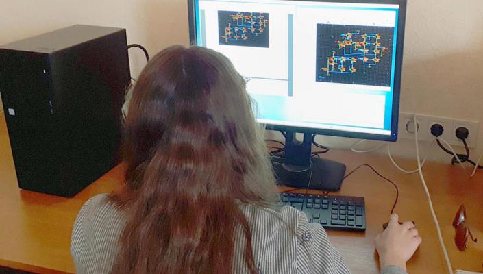
In January 2020, a laboratory for VLSI analog design was opened at the Department of Electronic Engineering, Kyiv Polytechnic Institute (KPI). The project was implemented by joint efforts of KPI and partner companies, Tower Semiconductor, Israel, and Cadence Design Systems, USA, which provided hardware and software. The resources of the laboratory allow to conduct end-to-end design of analog chips from circuit design to topology development and analysis of the planned circuit taking into account parasitic effects.
The laboratory is a member of the Cadence Academic Network program, which brings together leading educational institutions and leading companies in the field of development and production of microelectronics. The laboratory is certified in Custom IC Design technology. Laboratory certification requires involvement of qualified teachers who have been trained and successfully passed the certification tests, as well as undergo annual training. Currently, the department has 4 certified teachers, 3 of whom have just confirmed their status for next year.
The quarantine restrictions introduced in March 2020 did not become an obstacle to learning. Appropriate network services have been deployed to organize remote work. Students and teachers have the opportunity to work from any place connected to the Internet.
In the spring semester of 2020, the 5th year students of the Department of Electronic Engineering were the first to study. They learned to work with schematic editor from Virtuoso System Design platform in a series of laboratory works with the help of manuals developed by teachers of the department. In addition, students took the opportunity to study on Cadence Internet Learning System (iLS), 12 of them received certificates of completion. Teachers of Microelectronics Department also completed their training, 2 associate professors received appropriate certificates.
In the autumn semester of 2021, the resources of the laboratory were used by 4th year students. In addition to the laboratory work provided by their program, students also expressed interest in online training, 14 of them received certificates of successful completion for Vistuoso Schematic Editor and Spectre simulator.
Leading force of the project, Tower Semiconductor, the leader in high-value analog semiconductor foundry solutions, was introduced through domestic design bureau UkrSemi, which employs graduates of Electronic Engineering Department. Tower provides world-class design enablement tools complementing its customizable process platforms such as SiGe, BiCMOS, mixed signal/CMOS, RF CMOS, CMOS image sensor, non-imaging sensors, integrated power management (BCD and 700V), and MEMS. Students in the program gain exclusive direct access to Tower’s analog process as reflected in the company’s PDK, allowing hands-on practical experience with silicon manufacturing. This year, UkrSemi welcomed 2 students for their undergraduate internship. They have chosen design of amplifier circuits for their graduation work. In addition to the internship of graduates, 4th year student took internship at UkrSemi as well. According to Tatiana: “I tried myself in developing a block of a real circuit - a level translator. Difficult, but extremely interesting. This is real electronics! ”
In the spring semester of 2021. 3rd year students will learn modeling and design tools. Third-year students of the Electronic Devices and Systems Department will also join the students of Electronic Engineering and Microelectronics Departments.

