


Feed aggregator
Silicon Photonics: Breaking the Bandwidth Barrier in AI Computing
Artificial intelligence now pushes computing beyond just processing power. In today’s large-scale AI systems using deep learning and transformer models, the main challenge is efficiently moving data across complex, distributed systems.
In Hyperscale data centres and high-performance AI clusters, thousands of GPUs and accelerators run in parallel, constantly exchanging data. As models and datasets grow, electrical interconnects reach physical limits on bandwidth, power consumption, and thermal management.
The industry faces a turning point. Sustaining AI’s next growth phase needs new interconnect technology. Silicon photonics, which uses light rather than electrical signals, is becoming essential to this shift.
From Electrons to Photons: Rethinking Interconnect ArchitectureSilicon photonics introduces a paradigm shift by replacing conventional electrical signalling with optical communication. By integrating photonic components such as waveguides, modulators, and photodetectors onto silicon substrates using CMOS-compatible processes, it becomes possible to align optical communication with existing semiconductor manufacturing ecosystems.
Following this integration, optical interconnects offer clear structural advantages over traditional copper-based systems: Higher bandwidth density without proportional increases in physical complexity.
- Reduced signal degradation over longer distances
- Immunity to electromagnetic interference
Building on these benefits, a critical technique in this domain is wavelength-division multiplexing (WDM), which enables multiple data streams to be transmitted simultaneously over different wavelengths through a single optical channel. This significantly enhances throughput while maintaining manageable interconnect density.
The broader industry shift toward data-centric system design reflects a growing recognition that communication efficiency is now as important as compute performance. As Jensen Huang has noted, “The future of computing is about moving data faster and more efficiently than ever before.” This perspective underscores the growing importance of interconnectivity in AI systems.
Scaling AI Workloads: The Limits of Electrical InterconnectsModern AI workloads are distributed. Training large models needs coordinated computation across accelerator clusters with ongoing data exchange. This strains the interconnect infrastructure.
Electrical interconnects are widely used but face scaling limits. Bandwidth saturates at higher data rates due to signal integrity.
- Disproportionate increases in power consumption with higher throughput
- Thermal challenges arising from dense, high-speed electrical signalling
Silicon photonics solves these issues with high-bandwidth, lower-energy communication. Optical signals carry more data efficiently and reduce losses from resistance and heat.
This transition is not merely an incremental upgrade; it reflects a structural evolution in system architecture. As Sundar Pichai has emphasised, “The opportunity with AI is as big as it gets.” Realising that opportunity depends on overcoming infrastructure bottlenecks, particularly those related to data movement.
Energy Efficiency: A Defining Constraint in AI InfrastructureAs AI systems scale, energy efficiency has become a primary engineering concern. Data centres supporting AI workloads are experiencing rapid increases in power demand, with interconnects contributing significantly to overall energy consumption.
Silicon photonics offers a pathway to improved efficiency by reducing the energy required to transmit each bit of data. Optical communication minimizes resistive losses and reduces the need for repeated signal amplification, particularly over longer distances.
This results in several system-level benefits:
- Lower operational energy consumption in large-scale deployments
- Reduced thermal load and simplified cooling requirements
- Improved sustainability metrics for data center operations
The importance of energy-efficient infrastructure is widely acknowledged across the industry. As Satya Nadella has stated, “Every data center must become more energy efficient as AI scales globally.” Silicon photonics directly supports this objective by enabling high-performance communication with lower power overhead.
Co-Packaged Optics: Integrating Compute and CommunicationA significant architectural development enabled by silicon photonics is the emergence of co-packaged optics (CPO). Unlike traditional pluggable optical modules, CPO integrates optical components directly alongside compute silicon within the same package.
This approach reduces the distance between processing and communication layers, enabling tighter system integration and improved performance. The advantages include reduced latency, higher interconnect density, and the elimination of many electrical I/O bottlenecks.
While alternative approaches—such as advanced packaging and chiplet-based architectures continue to evolve, they primarily extend the capabilities of electrical interconnects rather than overcoming their fundamental limitations. Silicon photonics, by contrast, addresses the underlying physics constraints, offering a more scalable path forward for AI infrastructure.
From Research to Deployment: Growing Industry MomentumSilicon photonics is transitioning from research laboratories to real-world deployment. Hyperscale data centres are increasingly incorporating optical interconnects to handle high-volume, low-latency communication across servers and racks.
Its relevance spans multiple application domains, including AI training clusters, high-performance computing environments, telecommunications networks, and emerging edge AI systems. Across these domains, the common requirement is efficient, high-speed data movement.
The growing investment from semiconductor and technology companies reflects a broader industry shift. Silicon photonics is no longer a speculative technology; it is becoming an operational necessity for scaling AI systems.
Engineering Challenges: Bridging Innovation and ImplementationDespite its advantages, silicon photonics presents several engineering challenges that must be addressed to enable widespread adoption.
- Integration complexity in co-designing photonic and electronic components
- Sensitivity of optical elements to temperature variations
- Challenges associated with efficient on-chip laser integration
- Manufacturing variability affecting large-scale production consistency
Addressing these issues requires coordinated innovation across design methodologies, fabrication processes, and system-level validation techniques. The transition to photonic interconnects is not solely a technological shift it also demands ecosystem maturity.
Future Outlook: Toward Photonics-First ArchitecturesLooking ahead, silicon photonics is expected to play a central role in the evolution of AI infrastructure. As distributed computing becomes the norm and model complexity continues to grow, efficient data movement will remain a critical requirement.
Emerging directions include on-chip optical interconnects, hybrid electronic-photonic systems, and new computing paradigms that leverage photonic principles for ultra-fast data processing. These developments point toward a long-term transition in which optical technologies become central to hardware design. This is not a peripheral enhancement; it is a foundational transformation.
As Elon Musk has remarked in the broader context of computing innovation, “The pace of innovation must accelerate to keep up with AI.” Achieving that acceleration will depend not only on advances in algorithms but also on the underlying hardware systems that enable them.
Conclusion: Redefining the Foundations of AI InfrastructureIn the evolution of artificial intelligence, the industry is confronting a fundamental shift: compute capability alone is no longer sufficient. The efficiency of data movement has become equally critical in determining system performance and scalability.
Silicon photonics represents a decisive step toward addressing this challenge. Overcoming the limitations of electrical interconnects enables architectures that are faster, more energy-efficient, and better suited to the demands of modern AI workloads.
This is not a peripheral enhancement; it is a foundational transformation. As AI systems continue to scale and become more complex, silicon photonics is poised to become a cornerstone of next-generation computing infrastructure, shaping how intelligent systems are built and deployed in the years ahead.
The post Silicon Photonics: Breaking the Bandwidth Barrier in AI Computing appeared first on ELE Times.
PLC, PAC, and Industrial PC Architectures for Automation
Introduction
Industrial automation is undergoing a fundamental transformation. Traditional control systems designed primarily for machine sequencing and process control are now expected to support advanced analytics, predictive maintenance, artificial intelligence (AI), digital twins, cloud connectivity, and cybersecurity frameworks. As manufacturing and infrastructure systems become increasingly data-intensive, engineers face a critical challenge: selecting the most appropriate control architecture.
For decades, the Programmable Logic Controller (PLC) was the undisputed backbone of industrial automation. Later, Programmable Automation Controllers (PACs) emerged to bridge the gap between deterministic control and information processing. Today, Industrial PCs (IPCs) have evolved into powerful edge-computing platforms capable of running sophisticated automation software alongside AI and data analytics workloads.
The boundaries between these technologies are becoming increasingly blurred. Modern PLCs offer edge computing capabilities, PACs provide PC-like processing power, and industrial PCs deliver real-time deterministic control. Consequently, selecting the right controller is no longer about choosing the “best” technology but about understanding engineering requirements, operational constraints, and lifecycle considerations.
Understanding the Architectural Differences
PLC: The Deterministic Workhorse
PLCs were designed specifically for industrial environments where reliability and deterministic operation are paramount. Their architecture is optimized for real-time control tasks, including discrete I/O management, sequencing, interlocking, and safety functions.
Typical PLC architecture includes:
- Dedicated real-time operating systems
- Ruggedized hardware
- Scan-cycle execution model
- Integrated digital and analog I/O
- Long operational life cycles
- High resistance to electrical noise and harsh environments
The PLC continuously executes a control loop consisting of:
- Input scan
- Logic execution
- Output update
- Communication services
This deterministic behavior makes PLCs ideal for packaging machines, conveyor systems, assembly lines, water treatment plants, and utility infrastructure.
Key Strength: Predictable control performance with extremely high reliability.
Limitation: Limited computational capability for data-intensive applications.
PAC: Bridging Control and Information
Programmable Automation Controllers emerged as industrial systems became more complex and interconnected.
PACs combine the deterministic nature of PLCs with the flexibility of modern computing platforms. Unlike traditional PLCs, PACs support:
- Multi-domain automation
- Advanced motion control
- Large memory capacity
- Object-oriented programming
- Integrated networking
- Database connectivity
PACs generally comply with IEC 61131-3 standards while supporting higher-level software architectures.
Industrial PC: The Data-Centric Controller
Industrial PCs bring standard computing power into the industrial environment.
Modern IPCs feature:
- Multi-core processors
- High-capacity memory
- Solid-state storage
- Virtualization support
- AI acceleration
- GPU integration
- Industrial communication interfaces
Unlike PLCs, IPCs typically run:
- Windows
- Linux
- Real-Time Linux
- Hypervisor-based architectures
The rise of Industry 4.0 has significantly increased IPC adoption because they can process massive datasets locally while maintaining cloud connectivity.
Engineering Decision Framework
Instead of asking, “Which controller is better?” engineers should ask the following questions:
- How Critical Is Deterministic Performance?
Applications such as:
- Emergency shutdown systems
- Turbine control
- Motion synchronization
- Safety systems
require guaranteed response times.
In such cases, PLCs and PACs remain the preferred solutions.
- How Much Data Must Be Processed?
Modern smart factories generate terabytes of operational data.
Applications involving:
- AI-based inspection
- Video analytics
- Condition monitoring
- Predictive maintenance
often exceed traditional PLC capabilities and favour Industrial PCs.
- What Is the Environmental Requirement?
PLCs generally provide the highest environmental resilience, although ruggedized IPCs continue to improve.
- What Is the Expected Lifecycle?
Many manufacturing facilities expect automation assets to operate for decades.
PLC vendors often provide long-term support and product availability, making them attractive for infrastructure projects with extended service lives.
Industrial PCs may require more frequent hardware refresh cycles.
- What Are the Cybersecurity Requirements?
As operational technology (OT) becomes connected to enterprise IT networks, cybersecurity has become a critical design consideration.
Industrial PCs running conventional operating systems introduce a larger attack surface than dedicated PLC platforms.
Engineers must evaluate:
- Patch management
- Network segmentation
- Secure boot
- Endpoint protection
- Zero-trust architectures
before selecting a controller platform.
Emerging Hybrid Architectures
The most significant trend in industrial automation is convergence.
Leading automation vendors are increasingly integrating PLC, PAC, and IPC technologies into unified architectures.
Companies such as Siemens, Rockwell Automation, Schneider Electric, Beckhoff Automation, and Bosch Rexroth are investing heavily in software-centric automation architectures that blur traditional controller boundaries.
In many modern facilities, the architecture is no longer PLC versus IPC. Instead, PLCs provide deterministic machine control while Industrial PCs handle AI, visualization, and analytics at the edge. PACs often serve as the integration layer between these domains.
The Future: Software-Defined Industrial Control
The next generation of automation systems will increasingly separate software from hardware.
Virtualized controllers running on industrial servers are beginning to challenge conventional hardware-based automation architectures. AI-assisted engineering tools, digital twins, and edge computing platforms will continue driving demand for more computationally capable control systems.
However, deterministic control remains the foundation of industrial automation. Regardless of future innovations, the engineering challenge will continue to revolve around balancing reliability, performance, security, scalability, and cost.
Conclusion
The debate between PLCs, PACs, and Industrial PCs is no longer a simple technology comparison. Each architecture serves a distinct purpose within modern automation ecosystems.
For today’s engineers, the optimal solution is increasingly a hybrid architecture that combines the strengths of all three platforms. Success lies not in choosing a single controller type but in understanding the specific operational requirements and designing a system architecture that balances control integrity with digital innovation.
As factories evolve toward autonomous, connected, and intelligent operations, the future belongs to architectures that seamlessly integrate deterministic control with data-driven intelligence.
The post PLC, PAC, and Industrial PC Architectures for Automation appeared first on ELE Times.
Optics and Silicon Photonics: The Next Data Highway Inside Chips
For more than five decades, the semiconductor industry has relied on a simple principle: increasing transistor density to deliver higher computing performance. While transistor scaling continues to advance, a new bottleneck has emerged inside modern computing systems—data movement.
Today’s processors, AI accelerators, memory systems, and data centers spend a significant portion of their energy simply moving data through metallic interconnects. Traditional copper wiring, which has served electronics faithfully for decades, is rapidly approaching its physical limitations. Resistance, capacitance, signal attenuation, electromagnetic interference, and heat generation increasingly constrain performance.
To overcome these challenges, the semiconductor industry is turning toward a revolutionary solution: Silicon Photonics. Instead of electrons traveling through copper traces, future chips will increasingly use photons—particles of light—to carry information. The result could be processors capable of transferring data at unprecedented speeds while consuming significantly less power and generating far less heat.
What is Silicon Photonics?: Silicon Photonics is a technology that integrates optical communication components directly onto silicon chips using semiconductor manufacturing processes similar to those used for CMOS integrated circuits.
Instead of transmitting information via electrical signals, silicon photonic devices use light waves traveling through microscopic optical waveguides fabricated on silicon wafers.
A typical silicon photonic system consists of:
- Lasers
- Optical modulators
- Waveguides
- Multiplexers
- Photodetectors
- Electronic control circuits
Together, these components allow information to be converted from electrical signals into optical signals and back again.
For working engineers, the story is no longer just about making transistors smaller. It is about moving data fast enough to keep up with them. As electrical links stretch across boards, packages, and racks, copper starts to run into familiar physical problems: resistance, crosstalk, signal loss, heat, and rising power cost per bit. Silicon photonics answers that bottleneck by carrying information as light rather than electrons, using optical links to push bandwidth higher while reducing the energy spent on interconnects. In practice, that makes photonics one of the most important enabling technologies for AI systems, HPC clusters, and data-center networking.
The engineering shift is straightforward in concept and hard in implementation. A silicon photonics platform integrates optical devices with standard CMOS-style manufacturing so data can be modulated, routed, and detected on or near the chip package. Intel describes its platform as combining silicon manufacturing scale with light on a single chip, and says its solutions now span 400G, 800G, and 1.6T-class interfaces. Ayar Labs takes a similar direction with optical I/O chiplets, positioning them as a low-power, low-latency alternative to copper backplanes and pluggable optics.
The practical reason this matters is bandwidth density. When systems scale from a handful of accelerators to dense AI fabrics, the bottleneck is often not compute silicon itself but how quickly data can enter, leave, and circulate around it. That is why the industry is moving from pluggable transceivers toward co-packaged optics, where optical engines sit much closer to the switch ASIC or accelerator package. NVIDIA says its silicon-photonics-based networking is aimed at this problem, with its 2025 Spectrum-X Photonics announcement targeting scale-out AI factories and claiming major gains in energy efficiency and resiliency. Broadcom is also pushing co-packaged optics and silicon-photonics chiplets for high-radix AI networks.
A useful way to think about the transition is this: copper is still excellent for short, simple, low-cost links, but it becomes expensive in power and signal integrity as reach and rate increase. Silicon photonics does not eliminate that tradeoff everywhere, but it moves the break-even point dramatically. Intel says its platform has already shipped more than 8 million photonic integrated circuits and more than 32 million on-chip lasers, while NVIDIA and Broadcom are both anchoring their latest AI networking roadmaps around photonics and co-packaged optics.
For engineers, the opportunity is not just faster links; it is system design freedom. Optical interconnects can relax board routing constraints, reduce electrical retiming overhead, and help keep power budgets under control as data rates climb. That is why the near-term adoption path is strongest in the I/O layer, package-to-package links, switch fabrics, and rack-scale interconnects, where the cost of moving bits is becoming as important as the cost of computing them. The architecture of future systems will still be electronic at the logic core, but increasingly optical at the boundaries where data movement hurts most.
In short, silicon photonics is not a futuristic side project anymore. It is becoming a serious engineering answer to a very present problem: how to keep AI, HPC, and networking systems from drowning in their own data traffic. The companies most visibly shaping the field today include Intel, NVIDIA, Ayar Labs, and Broadcom, each attacking the same bottleneck from a slightly different angle. For engineers building the next generation of systems, photonics is moving from “interesting” to “necessary.”
The semiconductor industry’s next breakthrough may not come solely from smaller transistors, but from replacing electrons with photons for data movement. As copper interconnects approach fundamental physical limits, silicon photonics offers a path toward dramatically higher bandwidth, lower latency, and significantly improved energy efficiency.
For working engineers, the transition to photonic computing represents more than an incremental improvement—it signals a fundamental architectural shift in how information is transported within and between computing systems. Companies such as Intel, NVIDIA, Cisco, Broadcom, Ayar Labs, Lightmatter, and Celestial AI are already laying the foundation for this future.
Over the coming decade, optical interconnects, co-packaged optics, and photonic processors are expected to become core enabling technologies for AI supercomputers, hyperscale data centers, and next-generation embedded systems. Just as silicon transformed computing in the twentieth century, silicon photonics may define the computational infrastructure of the twenty-first century.
The post Optics and Silicon Photonics: The Next Data Highway Inside Chips appeared first on ELE Times.
Neuromorphic Engineering & Edge AI: The Future of Intelligent Computing
Artificial Intelligence is rapidly transforming industries, but traditional AI systems come with a major challenge: enormous energy consumption. Most modern AI applications depend on cloud-based data centers packed with power-hungry GPUs and servers. As billions of smart devices become connected, this centralized approach is becoming increasingly expensive, slower, and environmentally unsustainable.
A revolutionary solution is emerging through Neuromorphic Engineering and Edge AI. Instead of relying entirely on distant cloud servers, scientists and engineers are building specialized chips that mimic the structure and behavior of the human brain. These advanced processors, known as neuromorphic chips and AI accelerators, process information directly on devices such as smartphones, drones, medical wearables, robots, and autonomous vehicles. This approach dramatically reduces latency, improves privacy, and cuts energy consumption.
What is Neuromorphic Engineering?
Neuromorphic engineering is a field that designs computer hardware inspired by biological neural systems. Traditional computers process data sequentially and continuously, even when there is little meaningful activity. The human brain, however, operates differently. Neurons only “fire” when necessary, making the brain remarkably energy efficient while handling complex sensory information in real time.
Neuromorphic chips attempt to replicate this behavior using Spiking Neural Networks (SNNs). Unlike conventional neural networks that constantly process streams of data, SNNs activate only when changes occur. This event-driven architecture significantly reduces unnecessary computation and power usage.
Brain-Inspired AI Hardware
Modern neuromorphic processors integrate memory and computing together instead of separating them like traditional CPU and GPU architectures. This eliminates the “von Neumann bottleneck,” where large amounts of energy are wasted transferring data between memory and processors.
Companies and research institutions worldwide are developing advanced neuromorphic systems. Intel’s Loihi 2 chip, for example, can simulate millions of neurons while consuming only a fraction of the energy used by traditional AI hardware. Some experimental chips operate in milliwatts rather than watts, making them ideal for portable and battery-powered devices.
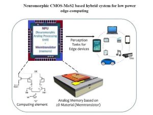
Researchers are also exploring technologies such as memristors, which combine memory and processing in a single component, closely resembling biological synapses. These innovations could eventually enable AI systems that learn continuously and adapt in real time without relying on cloud computing.
The Rise of Edge AI
Edge AI refers to running artificial intelligence directly on local devices rather than sending data to centralized servers. Today, many AI applications depend on cloud infrastructure, which introduces delays and requires constant internet connectivity. Edge AI changes this model by bringing intelligence closer to the source of data.
For example:
- Self-driving cars must make decisions instantly without waiting for cloud responses.
- Smart surveillance cameras need real-time object recognition.
- Wearable healthcare devices must continuously monitor vital signs with minimal battery drain.
- Industrial robots require rapid reactions in manufacturing environments.
Neuromorphic processors are particularly well-suited for these applications because they deliver near-zero latency and ultra-low power consumption.
Energy Efficiency and Sustainability
One of the biggest advantages of neuromorphic computing is energy efficiency. Conventional AI training and inference systems consume massive amounts of electricity. Data centers supporting generative AI models now require enormous cooling systems and power grids. Neuromorphic systems dramatically reduce this burden. According to recent studies, some neuromorphic architectures can achieve over 100 times better energy efficiency compared to traditional deep learning hardware.
The human brain itself consumes only about 20 watts of power — less than a dim light bulb — while performing tasks that remain challenging for modern computers. Neuromorphic engineers aim to approach this extraordinary level of efficiency. This has major implications for sustainable computing. As global AI adoption accelerates, reducing energy demand will become essential for lowering operational costs and minimizing environmental impact.
Real-World Applications
Neuromorphic Edge AI is already finding applications across multiple industries:
Healthcare
Wearable devices powered by neuromorphic chips can continuously monitor patient conditions, detect abnormalities, and even predict medical emergencies with minimal battery usage.
Autonomous Vehicles
Self-driving systems require split-second decisions. Neuromorphic processors enable rapid sensor processing for safer navigation and collision avoidance.
Robotics
Robots equipped with brain-inspired AI can react more naturally to changing environments while consuming far less energy.
Defense and Aerospace
Low-power edge computing is critical for drones, radar systems, and satellites operating in remote environments.
Consumer Electronics
Future smartphones, AR glasses, and smart home devices may run advanced AI locally without depending heavily on cloud services.
Challenges Ahead
Despite its promise, neuromorphic computing is still in its early stages. Developing efficient training methods for spiking neural networks remains difficult, and software ecosystems are less mature than traditional AI frameworks. Manufacturing specialized hardware at scale is another challenge. However, rapid advances in semiconductor technology and growing demand for sustainable AI are accelerating innovation in this field.
Conclusion
Neuromorphic Engineering and Edge AI represent a major shift in the future of computing. By mimicking the brain’s architecture, these technologies enable intelligent devices that are faster, smarter, and far more energy efficient than traditional systems. As AI continues to expand into every aspect of daily life, neuromorphic chips could become the foundation for a new generation of sustainable, low-latency, and autonomous technologies. The future of AI may no longer reside solely in giant cloud data centers — it may live directly inside the devices we use every day.
The post Neuromorphic Engineering & Edge AI: The Future of Intelligent Computing appeared first on ELE Times.
Ensuring Reliable AI in Safety-Critical Systems: Challenges and Engineering Solutions
In safety-critical environments, reliability is paramount, and errors have immediate, real-world consequences. If an autonomous system falters in urgent decisions, a clinical support tool misguides diagnoses, or an industrial controller fails in hazardous conditions, the results can be life-threatening. Artificial intelligence must be unwaveringly accurate and reliable at every moment to ensure safety and maintain trust in deployment.
This demands a fundamental shift in AI system engineering. Unlike traditional domains, where model accuracy or benchmark performance may suffice, safety-critical applications require predictable, consistent, and fail-aware behaviour across diverse conditions. The real challenge is to establish AI as fundamentally trustworthy in situations where failure is not an option, making reliability, not just intelligence, the core success criterion.
As AI integrates into mission-critical infrastructure, reliability is not just a technical requirement; it is the foundation and defining goal for deploying AI in safety-critical systems.
The Reliability Gap: From Probabilistic Models to Deterministic ExpectationsA core engineering challenge now demands urgent attention: a deep mismatch exists between traditional system design and modern AI behaviour. Safety-critical systems have historically been deterministic, producing predictable and verifiable outputs. In stark contrast, AI models are inherently probabilistically trained on data, influenced by variability, and alarmingly sensitive to environmental changes.
This mismatch creates a reliability gap that cannot be ignored in high-stakes deployments:
- High accuracy does not ensure safe behaviour in rare or unseen scenarios
- Models may generate confident yet incorrect predictions
- Behaviour under edge conditions remains difficult to anticipate
In safety-critical contexts, such uncertainties quickly become intolerable. Systems must now be engineered not just for performance, but for rigorous assurance under uncertainty. As Sundar Pichai warned, “The more capable AI becomes, the more critical it is to ensure it behaves safely and predictably.” This is no longer a theoretical challenge; it is the defining engineering crisis of our time.
Core Challenges in Deploying Reliable AI SystemsThe dynamic nature of real-world environments directly undermines reliability. AI systems trained in controlled settings inevitably confront distribution shifts at deployment scenarios absent from training data. These shifts degrade performance, especially in rare or safety-critical contexts.
In addition to distribution shifts, another critical issue is the inability of many models to communicate uncertainty. AI systems often produce outputs with high confidence, even when operating outside their domain of competence. In applications involving autonomous control or real-time decision-making, such overconfidence can lead to unsafe outcomes without warning.
Building on the previous concern, explainability is equally important. Safety-critical systems demand traceability and accountability, yet many AI models function as opaque decision-makers. Without the ability to interpret decisions, validating system behaviour and meeting regulatory expectations becomes significantly more difficult.
Finally, AI systems do not operate in isolation. They are part of a broader ecosystem involving sensors, embedded hardware, and control systems. Variability at any of these levels, whether due to sensor noise, latency, or hardware constraints, can influence overall system reliability. Ensuring dependable operation, therefore, requires a holistic, system-level perspective.
When AI Fails: Understanding System-Level RiskFailures in safety-critical AI systems are rarely isolated events. A single incorrect output can propagate across the system, leading to cascading effects that compromise overall functionality.
The most critical risks include:
- Silent failures, where incorrect outputs remain undetected
- Error propagation across interconnected system components
- Over-reliance on AI outputs, reducing effective human oversight
These risks highlight a key engineering principle: reliability must be designed into the system from the outset. It cannot be treated as a post-deployment evaluation metric.
Engineering Reliable AI: From Models to SystemsWe must shift from model-centric development to system-level assurance to address these challenges. We need to embed reliability across the entire lifecycle, from data collection to deployment and monitoring.
A foundational step is robust data engineering. Expand datasets to capture real-world variability. Simulate edge-case scenarios. Continuously monitor for data drift. These approaches improve generalisation and reduce unexpected system behaviour.
Equally important is uncertainty-aware system development. Integrate mechanisms that estimate prediction confidence so that models detect when they exceed their limits. This enables fallback strategies, like deferring to human operators or switching to safe modes. In this way, AI evolves from static prediction to self-aware system components.
Validation methodologies must also evolve. Traditional testing approaches are insufficient for capturing the complexity of AI behaviour. Scenario-based testing, simulation of rare or hazardous conditions, and stress testing under extreme inputs are becoming essential tools for evaluating reliability beyond standard datasets.
Explainability strengthens system assurance. While full transparency is rare, interpretable insights enable debugging, validation, and regulatory compliance. These capabilities help build trust among stakeholders.
Redundancy plays a central role in ensuring reliability. Instead of relying on a single model, systems increasingly incorporate multiple validation layers, hybrid architectures combining AI with rule-based logic, and predefined fail-safe states. As Satya Nadella emphasises, “Trust must be built into every layer of AI systems.” Redundancy ensures that this trust does not depend on a single point of failure.
System-Level Assurance: Beyond the AlgorithmA key realisation in modern engineering is that AI reliability cannot be isolated to the model alone. True assurance requires coordination across the entire system stack, including data pipelines, inference mechanisms, hardware platforms, and control logic.
This has led to the emergence of hardware-software co-design, where AI models are optimised alongside the systems that execute them. In this paradigm, reliability becomes a property of the entire system rather than an attribute of the algorithm alone.
Industry Perspective: Measured Adoption in High-Stakes DomainsAI adoption in safety-critical industries is cautious, driven by the persistent gap between experimental results and proven, production-level reliability.
Organisations are prioritising validation, risk mitigation, and incremental integration over rapid deployment. Hybrid approaches combining AI capabilities with deterministic safeguards are becoming increasingly common, reflecting the need to balance innovation with operational safety.
Regulatory and Certification ChallengesRegulatory frameworks for safety-critical systems were originally designed for deterministic software. Applying these frameworks to AI introduces significant challenges, particularly in verifying non-deterministic behaviour and defining acceptable risk thresholds.
The absence of standardised validation methodologies further complicates certification processes. As a result, the industry is moving toward new assurance models that emphasise transparency, traceability, and continuous validation throughout the system lifecycle.
Future Outlook: Toward Assured and Certifiable AIThe future of AI in safety-critical systems demands convergence. Data-driven intelligence will be fused with rule-based safeguards, and machine learning models will be integrated decisively with formal verification techniques.
Building on this convergence, continuous monitoring and adaptive system design will decisively enhance reliability, ensuring systems respond dynamically to changing conditions. We will deliver not just intelligent systems, but AI that is verifiably safe and certifiable for deployment.
As Jensen Huang states, “AI is advancing rapidly, but reliability and safety must scale with it.” This balance will define the next phase of AI engineering.
Conclusion: Reliability as the Foundation of Trustworthy AIAs AI expands into safety-critical domains, the definition of success is being redefined. Performance alone is no longer sufficient. Systems must demonstrate predictable behaviour under uncertainty, transparency in decision-making, and resilience in the face of failure.
AI must be engineered as a dependable system component, fully integrated into a broader safety and assurance framework. In this evolving landscape, reliability is not an added feature; it is the foundation upon which trust is built.
The trajectory of AI in safety-critical systems hinges not just on intelligence, but on how reliably these systems earn trust when it matters most.
The post Ensuring Reliable AI in Safety-Critical Systems: Challenges and Engineering Solutions appeared first on ELE Times.
Nanometer Nanotubes for Future Electronics
Researchers in Japan creates the world’s smallest semiconducting nanotubes, structures 100,000 times thinner than a human hair. By growing molybdenum disulfide inside protective tubes of boron nitride, researchers, including those from the University of Tokyo, produce highly uniform tubes just 1 nanometer wide, a scale at which it’s difficult to make stable nanotube structures. The work confirms decades-old theoretical predictions about how these ultrafine materials behave and could also provide a new route toward miniaturized electronic devices.
A few years back, carbon nanotubes were attracting a lot of press attention. But there’s a new contender in the ring, and it offers some advantages over its carbon counterpart that could tempt engineers to design products around it. Molybdenum disulfide (MoS2) nanotubes, though still experimental in nature, point to applications in semiconductor electronics, high-resolution sensing, and quantum-scale physics research.
“We achieved the synthesis of atomically precise semiconducting nanotubes with nanometer diameters. The coaxial structure, where a semiconducting MoS2 nanotube is surrounded by an insulating boron nitride (BN) nanotube, is attractive for gate-all-around transistors, one of the most advanced transistor architectures,” said Associate Professor Yusuke Nakanishi from the Department of Advanced Materials Science at the University of Tokyo. “Our paper demonstrates a way for structural control of inorganic semiconducting nanotubes at the atomic scale. And we experimentally demonstrated that the bandgap (related to how materials work as semiconductors) of the nanotubes decreases as their diameters become smaller, in agreement with theoretical predictions proposed more than a quarter century ago.”
Conventional methods for producing nanotubes are usually limited to diameters above 10 nanometers, multiwall concentric tubes, and poorly controlled or irregular atomic structures. Nakanishi and his team synthesized 1-nanometer-wide, single-wall MoS2 nanotubes with well-defined atomic structures. It manages the use of chemical reactions inside the narrow space of BN nanotubes. The confined space constrains the MoS2 nanotubes, which would otherwise be difficult to form, and promotes well-defined atomic arrangements, essential for engineered applications.
“In nanotubes, even small structural differences can strongly affect their properties. If the structure can be precisely controlled, the properties are more consistent, which is essential for reliable and reproducible transistor performance. Their biggest advantage is atomic-level structural control,” said Nakanishi. “Current silicon transistors are typically made by etching bulk silicon, but it’s increasingly difficult to keep their structures perfect at smaller sizes, where defects have a big impact. Carbon nanotubes also face a challenge for transistor applications, since even tiny structural differences can change how they behave, including whether they act more like metals or semiconductors. Our nanotubes could offer a more reliable way to build ultrasmall semiconductor channels with consistent properties.”
Practical applications are likely still some years away, and important challenges remain before working transistor devices can be made. In particular, the team wishes to increase the nanotube length from the current limit of several hundred nanometers to around 1 micrometer (which is 1,000 nanometers, and one-thousandth of a millimeter). Another future direction relates to materials: The method could also enable other inorganic nanotubes, including magnetic and superconducting materials. The researchers hope the work will help expand nanotube science beyond carbon-based systems and open the door to a broader class of atomically accurate nanotube materials for research, sensing, and smaller, faster devices.
The post Nanometer Nanotubes for Future Electronics appeared first on ELE Times.
TIL about SLP - Substrate-Like PCB Technology
 | submitted by /u/1Davide [link] [comments] |
Progress V2 -> V3 on our Open Access Health Tracker
 | 4 months ago I shared the progress of our Open Access Health Tracker from V1 to V2. Today I wanted to share the progress from V2 to V3 on a schematic level. And it's massive. 3x3cm PCB, 3 meters of traces and maxing the capabilities of JLCPCB. Plus an additional 2-3 PCBs for sensors not shown. Next up SLP instead of PCB. [link] [comments] |
Weekly discussion, complaint, and rant thread
Open to anything, including discussions, complaints, and rants.
Sub rules do not apply, so don't bother reporting incivility, off-topic, or spam.
Reddit-wide rules do apply.
To see the newest posts, sort the comments by "new" (instead of "best" or "top").
[link] [comments]
Automatic turntable that I'm designing from scratch
 | I'm designing a fully-automatic turntable from scratch called the Statimatic STM-01, using: - A Teensy 4.1 - Stepper for tonearm elevation - Stepper for tonearm azimuth movement - Stepper for azimuth clutch - Demultiplexer, to split elevation/azimuth stepper signal - Multiplexer, to handle input buttons (like "play" or "pause") - Shift register, to handle output LED statuses The "turntable" part isn't finished yet (nor is the automatic movement), so I'm just using an AR-XA as the turntable for now. I like records, and I like making stuff, so I decided I wanted to make a turntable. I know it isn't practical, but hey, I'm having fun with it! Please excuse the absolute mess that is the wiring. It is open source, though I'm not sure if GitHub links count as self promotion, so I'll play it safe and leave that out. [link] [comments] |
Pages




![[link]](https://i.redd.it/gzhe8f2bwp5h1.png)