
Feed aggregator
Edge AI Chipsets: How On-Device Intelligence Is Reshaping Embedded System Design
The cloud-first model for embedded systems is becoming a legacy architecture. We’re moving away from simply piping data to remote servers and instead shifting the entire decision engine onto the bare metal. Driven by specialised Edge AI silicon-like NPUs and accelerated RISC-V cores, this evolution allows us to bake autonomous logic directly into sensors and controllers. In a production environment, on-device AI is a functional requirement, not a luxury. As NVIDIA CEO Jensen Huang noted in his 2025 GTC keynote, “The next wave is already happening… Robotics, which has been enabled by physical AI-AI that understands the physical world, is the new era,” marking a definitive shift toward intelligence that lives where the action occurs.
Here is why Several factors make on-device AI critical today:
- Solving Latency: In robotics or power-grid monitoring, a cloud round-trip is a system failure. You need deterministic, sub-millisecond responses that only local inference provides.
- Cutting the Bandwidth Tax: Constant streaming drains batteries and budgets. Local processing means we only transmit the “meaning,” not the raw noise, making massive IoT fleets cost-effective.
- Hardened Privacy: For medical or industrial IP, data in transit is a liability. Keeping telemetry on the silicon is the most effective way to ensure confidentiality. Cristiano Amon, CEO of Qualcomm, reinforces this, stating: “When you do the processing on the device, it’s immediate. You don’t have to wait. It’s private. It’s your data. It’s your personal graph that stays with you.
- True Autonomy: Your hardware shouldn’t brick when the Wi-Fi drops. Edge AI ensures the machine stays smart in remote or “noisy” environments.
These factors collectively make Edge AI an essential enabler of modern embedded intelligence.
Architectural Distinctions of Edge AI Chipsets
Edge AI chipsets differ from conventional microcontrollers (MCUs) and CPUs in architectural intent and operational efficiency. Core characteristics include:
- AI Accelerators (NPUs/VPUs): Dedicated engines built for neural-network inference (convolutions, matrix multiplications) that significantly exceed CPUs in speed and power efficiency.
- Heterogeneous SoC Architectures: A combination of CPU (control tasks), NPU (AI inference), and sometimes GPU (parallel processing), ensures optimised resource allocation across workloads.
- Model Optimisation: Deep learning models can be deployed on devices with limited resources without experiencing significant accuracy loss thanks to techniques like quantisation, pruning, and compression.
- Power & Thermal Management: Edge AI can function within stringent power and temperature constraints thanks to dynamic voltage and frequency scaling, low-power modes, and thermal improvements.
- Security & Reliability Features: Protection of sensitive operations-particularly in industrial deployments and critical infrastructure achieved through measures such as memory isolation, secure boot processes, and hardware-level tamper-resistant design.
By combining these features, edge-AI chipsets make intelligent behaviour feasible on devices previously incapable of complex decision-making.
Transforming Embedded System Design
The introduction of Edge AI fundamentally alters embedded system design:
- From Reactive to Cognitive Systems: Traditional embedded devices follow deterministic logic to detect defects, predict equipment failures and monitor the electronic equipment. Edge AI enables them to perceive, classify, and act autonomously.
- Real-Time Autonomy: With local inference, devices operate independently of cloud connectivity, critical for industrial, safety-critical, or remote applications.
- Distributed Intelligence & Scalability: Large IoT deployments can now distribute AI across nodes, reducing network load and ensuring real-time responsiveness.
- Energy and Bandwidth Efficiency: Local processing cuts down on data transmission, which saves energy and money and makes the system less reliant on centralized infrastructure.
- Cross-Layer Co-Design: Hardware-software co-design is now essential. Teams must optimise model architecture, memory allocation, runtime scheduling, and power management from the outset.
Edge AI thus transforms embedded systems from simple controllers into autonomous, intelligent agents capable of learning and decision-making.
Real-World Applications
Edge AI chipsets are already revolutionising multiple sectors:
- Industrial Automation & Smart Manufacturing: Vision-based defect detection, predictive maintenance, anomaly detection, and real-time monitoring of inverters, EV chargers, and SMPS.
- Embedded Vision & IoT: Smart cameras, object detection, robotics, drones, and smart sensors with on-device analytics.
- Consumer Electronics & Wearables: Offline voice recognition, gesture detection, and biometric authentication while preserving privacy.
- Energy & Power Electronics: Autonomous monitoring of power converters, predictive fault detection, and safety-critical decisions in EV and renewable energy systems.
- Agriculture & Remote Infrastructure: Edge AI sensors classify crop health, monitor environmental conditions, and operate autonomously in rural or low-connectivity areas.
These applications illustrate that Edge AI is no longer experimental – it’s a practical enabler for real-world intelligence in embedded systems.
Challenges and Considerations
While Edge AI presents opportunities, several challenges require careful engineering:
- Resource Constraints: Limited compute, memory, and power require model optimisation, which may impact accuracy or capability.
- Hardware Heterogeneity: Diverse SoCs and NPUs make deployment across platforms complex.
- Thermal and Power Management: Continuous inference can generate heat and consume power, impacting device lifespan.
- Security & Trust: Edge devices handling sensitive data must ensure secure boot, encryption, and tamper resistance.
- Model Lifecycle Management: Updating and maintaining models across fleets of devices, especially in remote locations, is a significant operational challenge.
- Design Complexity: Effective deployment demands collaboration between ML engineers, hardware designers, and embedded software developers.
Addressing these challenges is essential for scalable, robust, and efficient Edge AI implementations.
Emerging Trends & the Road Ahead
Edge AI chipsets are evolving rapidly:
- TinyML and Micro-Edge Devices: Ultra-low-power NPUs enable AI on minimal sensors and microcontrollers.
- Chiplet-Based Modular SoCs: Modular architectures combining CPUs, AI accelerators, and memory provide scalable, upgradeable solutions.
- Cross-Layer Automation: Improved toolchains for quantisation, pruning, scheduling, and deployment reduce manual tuning and accelerate development.
- Hybrid Edge-Cloud Models: On-device inference combined with federated learning or cloud aggregation balances autonomy with long-term model improvement.
- Enhanced Security: Trusted execution environments and secure hardware primitives protect distributed edge deployments.
These trends point toward embedded systems that are intelligent, autonomous, energy-efficient, and scalable across industries.
India’s Emerging Edge AI Ecosystem
India is rapidly contributing to the global Edge AI landscape. Startups and MNCs like Netrasemi, Mindgrove Technologies, InCore Semiconductors, and MosChip Technologies are developing edge-AI SoCs, NPUs, and embedded solutions tailored for industrial, automotive, and IoT applications. With government initiatives like Digital India and Make in India, combined with academic research, the country is fostering innovation in Edge AI for both domestic and global markets.
Conclusion
Edge AI chipsets are changing what we expect from embedded devices. Work that once had to be pushed to a central system can now be handled directly where the data is produced. This allows equipment to react immediately, even in environments where connectivity is unreliable or power is limited. Designing such systems is no longer just a matter of selecting a processor and writing code; it involves careful trade-offs between performance, power use, reliability, and long-term maintenance, with security built in from the start. As AI visionary Andrew Ng recently summarised, “The future AI wealth doesn’t belong to those who own the largest GPU clusters but to those who know how to use the smallest models to solve the most specific problems… Edge computing and small models are the wealth keys.
For engineers in the embedded domain, this is a practical turning point rather than a theoretical one. Devices are moving beyond fixed, single-purpose roles and taking on more responsibility within distributed setups. Edge AI enables the development of autonomous and efficient systems. These solutions deliver the consistent reliability required by various industries.
The post Edge AI Chipsets: How On-Device Intelligence Is Reshaping Embedded System Design appeared first on ELE Times.
Quantum-Safe Hardware: Why the Cybersecurity Deadline Is Closer Than the Quantum Breakthrough
The world’s digital infrastructure is quietly approaching a cryptographic inflexion point. For decades, global cybersecurity has relied on a small set of mathematical assumptions, most notably RSA and elliptic-curve cryptography. These assumptions underpin everything from cloud authentication and mobile networks to payment systems, defence communications, and digital identity. Quantum computing threatens not to weaken these foundations, but to invalidate them entirely.
What makes this transition uniquely dangerous is not the arrival of quantum computers themselves, but the mismatch between how fast cryptography can be broken and how slowly hardware trust systems can be replaced. This is not a software problem that can be patched overnight. It is a hardware lifecycle problem measured in decades. As quantum research accelerates and post-quantum cryptography standards solidify, a hard truth is emerging across the industry: quantum-safe hardware must be deployed well before quantum computers can break encryption. Waiting for certainty is, paradoxically, the fastest path to systemic insecurity.
From Mathematical Risk to Engineering Reality
Quantum computing represents a rare technological disruption where the threat is mathematically inevitable, not probabilistic. Shor’s algorithm does not weaken RSA or elliptic-curve cryptography; it nullifies them. Once fault-tolerant quantum computers emerge, today’s cryptographic foundations collapse outright. More critically, attacks need not be real-time: encrypted data captured today can be decrypted years later under the “harvest now, decrypt later” model.
As Ali El Kaafarani, CEO of PQShield, has consistently argued, the industry’s mistake is treating post-quantum cryptography as a future software upgrade rather than a present hardware engineering challenge. Once quantum decryption is possible, compromise is retroactive; you don’t lose today’s secrets, you lose yesterdays. This reality has shifted focus from cryptographic theory to what can be implemented in silicon. While many PQC schemes exist on paper, only a narrow set survives real-world constraints of memory, power, latency, and side-channel resistance. Lattice-based algorithms such as NIST-standardised Kyber and Dilithium are currently the most hardware-viable, though they still impose significant demands. Other approaches, like code-based cryptography, struggle with impractically large key sizes that overwhelm secure hardware resources.
Why Hardware, Not Software, Is the Real Battleground
Cryptography is enforced by hardware roots of trust, HSMs, secure elements, TPMs, SIMs, and embedded controllers that underpin secure boot, identity, and key protection. Post-quantum cryptography breaks the assumptions these systems were built on: larger keys and heavier computation quickly expose the limits of hardware optimised for RSA and ECC. While software can absorb this overhead, hardware-bound systems cannot.
This is where “crypto-agility” fractures. Many platforms claim algorithm agility, but in practice, it exists only at the firmware or API layer, not in silicon. As Todd Moore, Vice President of Data Security Products at Thales, has noted, true crypto-agility is about whether hardware can evolve without becoming a performance bottleneck. In high-throughput environments, first-generation “PQC-ready” hardware often works functionally but not economically, forcing a choice between degraded performance and early replacement. Crypto-agility is no longer a software feature; it is a physical property of hardware architecture.
The Myth of Universal Crypto-Agility
In response to quantum risk, many vendors describe their products as “crypto agile.” In practice, crypto-agility has often meant that software can be updated, while the underlying hardware remains fixed. That model is breaking down. True crypto-agility in the post-quantum era requires hardware that was designed with uncertainty in mind: spare compute capacity, flexible accelerators, sufficient secure memory, and firmware update paths that are themselves resistant to quantum attacks. Much of the hardware deployed today, particularly older HSMs and embedded roots of trust, does not meet this bar.
Newer platforms from vendors such as Thales and Entrust are moving toward genuinely post-quantum-ready architectures, but even here, the industry is candid that early PQC support is only a first step. In many environments, especially high-throughput systems like certificate authorities and telecom authentication servers, performance collapses when PQC is layered onto hardware never designed for it. The uncomfortable implication is that a significant portion of deployed cryptographic hardware will ultimately need physical replacement, not because it is insecure today, but because it cannot scale securely tomorrow.
The Long-Life Device Problem: Secure Boot and Identity
Quantum risk becomes existential when hardware is expected to remain trusted for 15–20 years. Industrial equipment, telecom infrastructure, vehicles, medical devices, and defence systems often outlive multiple cryptographic generations. If the firmware-signing keys protecting these systems become quantum-breakable mid-lifecycle, attackers gain the ability to install malicious updates that appear fully legitimate.
To address this, hardware designers are rethinking trust from the ground up. Secure boot chains are increasingly being designed around hybrid verification models, where classical and post-quantum signatures coexist during a long transition period. Device identity is shifting toward roots of trust that can support PQC natively, rather than bolting it on later.
Equally important is the ability to migrate trust anchors in the field. Hardware that cannot rotate its cryptographic identity without physical access becomes a liability the moment quantum attacks become practical. In this sense, quantum-safe hardware is no longer just a security feature; it is a prerequisite for product longevity.
Scale Changes Everything
Post-quantum cryptography is feasible at a small scale. The real challenge emerges at volume. Larger keys and signatures mean more data moving through networks, more bytes stored in certificates, and more cycles spent on verification. In isolation, these costs are manageable. At the scale of global telecom networks, payment systems, and cloud platforms, they become systemic.
Cloud providers have already found that naïve PQC deployment can inflate handshake sizes enough to affect latency and throughput. Telecom operators face similar issues in authentication signalling, where milliseconds matter. This is why hybrid cryptography combining classical and post-quantum algorithms has become the dominant near-term strategy. Hardware acceleration is the critical enabler here. When PQC is supported at the silicon level, much of the overhead becomes manageable. When it is not, performance penalties cascade across the system.
The Real Deadline No One Wants to Announce
Public timelines often place cryptographically relevant quantum computers in the early to mid-2030s. Internally, many security leaders plan as if the deadline is earlier. The reason is simple: hardware migration takes time. From design and validation to certification and deployment, replacing cryptographic hardware across critical infrastructure can take a decade. Waiting for definitive proof that quantum computers can break RSA guarantees that the response will come too late. A pragmatic consensus is forming across the industry. By the second half of this decade, all new cryptographic hardware procurement must be quantum-safe by design. By the end of the decade, high-value infrastructure must complete the transition. Anything beyond those risks turning today’s encrypted data into tomorrow’s breach archive.
As Marco Pereira, Global Head of Cybersecurity at Capgemini, has emphasised about quantum risk “Quantum readiness isn’t about predicting a date, it’s about managing irreversible risk. Every encrypted asset today could become tomorrow’s breach if organisations delay adopting post-quantum protections.
Quantum-safe hardware is not driven by fear of the unknown. It is driven by certainty that cryptography is bounded by physics, certainty that hardware lifecycles are slow, and certainty that data longevity outlasts algorithm lifetimes. The organisations that navigate this transition successfully will not be those that deploy post-quantum cryptography fastest in software, but those that redesign their hardware roots of trust early, with crypto-agility, scale, and long-term integrity at the core. In the quantum era, cybersecurity failures will not arrive with alarms or outages. It will arrive quietly, years after the data was first captured. The only winning strategy is to make that data permanently useless before the quantum key ever turns.
The post Quantum-Safe Hardware: Why the Cybersecurity Deadline Is Closer Than the Quantum Breakthrough appeared first on ELE Times.
SQL Server IoT 2025: Why It Matters for Embedded and OEM Systems
Courtesy: Arrow Electronics
The new SQL Server IoT 2025 is now available! If you build devices, appliances, or embedded systems that ship with a database inside, SQL Server IoT 2025 is worth a serious look. It brings the SQL Server 2025 engine into long-life, fixed-function products. You get the full engine, the same AI features, the same JSON and vector capabilities, and the same security improvements. The only difference is that it is packaged and licensed for OEM and embedded scenarios.
In my experience supporting embedded customers, the pattern is consistent. More data at the edge, tight security requirements, long product lifecycles, and pressure to support AI without adding cloud dependencies. SQL Server IoT 2025 helps you handle those problems without changing how you design your systems. You can use the same T-SQL, drivers, tools, containers, and development workflow.
AI where your device runs
The biggest change in SQL Server IoT 2025 is the built-in AI stack. The database now supports a native vector type, semantic search, hybrid search, and local or remote model execution. You can generate embeddings inside the engine, and you can run AI agents through a secure REST endpoint that SQL Server manages.
Nothing in this requires a cloud connection unless you choose to use one. You can keep models local by using Ollama or ONNX Runtime. You can also call cloud models through Azure OpenAI or OpenAI.
For embedded systems, this means you can build features that previously required a cloud round-trip. Examples include local anomaly detection, troubleshooting assistance, natural language search of manuals or logs, and smarter automation. If you already store your device data in SQL Server, the new vector features let you use that data immediately.
Security that matches modern requirements
The platform is secure out of the box. SQL Server IoT 2025 carries forward the security updates from SQL Server 2025. That includes TLS 1.3, TDS 8.0, PBKDF hashing, managed identities, and stricter defaults. This helps you ship hardware that is ready for audit and compliance checks. For teams in healthcare, manufacturing, or other controlled industries, this reduces significant design risk.
Performance improvements that help small systems
Most devices in the field run on constrained compute, so predictable behaviour underload becomes more important than raw horsepower. SQL Server IoT 2025 benefits from improvements like optimised locking, Lock After Qualification, tempdb governance, faster failover, and reduced contention during heavy workloads.
Your device can run more predictable workloads with fewer stalls. It starts faster, handles concurrency better, and gives you cleaner behaviour when something in the system misbehaves.
Better ways to move data out of the device
You also get Change Event Streaming, which pushes changes directly to Azure Event Hubs. The engine streams committed transactions without extra system tables. This helps when your design needs low-latency reporting or coordination with services outside the device.
If you use Microsoft Fabric, SQL Server IoT 2025 supports database mirroring directly into OneLake. That gives you a simple path to analytics or long-term storage without writing ETL code.
Developer workflow stays simple
Stability in the toolchain is just as important as stability in the engine. SQL Server IoT 2025 uses the same drivers, SSMS, VS Code extension, containers, and deployment workflow. You also get the new JSON type, JSON indexing, RegEx functions, Base64 utilities, and improved T-SQL functions that SQL Server 2025 introduces.
When an upgrade is worth it
If you are trying to decide whether this upgrade is worth it, these are the points that usually guide the decision:
- If your device is running SQL Server 2014 or 2016, you are past or near the end of mainstream support, and the extended support runway is shrinking fast. SQL Server IoT 2025 offers a long-life option with a modern engine, stronger security, and a cleaner feature set for long-term maintenance. You also get improvements like accelerated recovery, better indexing behaviour, and up-to-date drivers.
- If your product roadmap includes AI features or if customers are asking for analytics without sending data off the device, SQL Server IoT 2025 gives you a built-in way to handle that.
- If your company is standardising on Fabric or Azure Arc, IoT 2025 fits neatly into that architecture.
If your design team is trying to reduce custom code around queues, logs, or sync processes, IoT 2025 reduces that work.
The post SQL Server IoT 2025: Why It Matters for Embedded and OEM Systems appeared first on ELE Times.
Microchip Releases Plastic Transient Voltage Suppressors for A&D Applications
Microchip Technology announced the release of its JANPTX family of non-hermetic plastic Transient Voltage Suppressor (TVS) devices that meet the MIL-PRF-19500 qualification, offering high-reliability protection for aerospace and defence applications. These TVS devices are the first in the industry to achieve MIL-PRF-19500 qualification in a plastic package, offering engineers a lightweight, cost-effective solution without sacrificing stringent military performance requirements. The JANPTX product line is available in voltage ranges from 5V to 175V and includes five variants: JANPTX1N5555UJ, JANPTX1N5558UG, JANPTX1N5629AUJ, JANPTX1N5665AUG, JANPTX1N5907UG and JANPTX1N5907UJ.
With a high peak pulse power rating of 1.5 kW and clamping response times measured at less than 100 picoseconds in internal tests, the JANPTX family is designed to help ensure the safety and reliability of sensitive electronic components in demanding environments. Designed for surface mounting, these unidirectional TVS devices deliver protection against voltage transients such as lightning strikes, electrostatic discharge (ESD), and electrical surges.
Key Features of the TVS Devices
- Surface-mount unidirectional TVS design
- Can suppress transients up to 1,500W at 10/1000 µs
- Capable of clamping transients in less than 100 ps
- Working voltage range: 5V to 175V
- Military qualification: MIL-PRF-19500/716
- Equivalent hermetic packages available for surface mount and thru-hole
- Weight: ~0.25 grams
Development Tools
The JANPTX devices are supported by various SPICE models, which enable the virtual prediction and simulation of a circuit’s behaviour, eliminating the need for time-consuming physical prototyping and redesigns.
The post Microchip Releases Plastic Transient Voltage Suppressors for A&D Applications appeared first on ELE Times.
Týr-the-Pruner: Search-based Global Structural Pruning for LLMs
Courtesy: AMD
Key Takeaways:
- End-to-end global structural pruning: Týr-the-Pruner jointly optimises pruning and layer-wise sparsity allocation, avoiding two-stage global ranking pipelines.
- Multi-sparsity supernet with expectation-aware error modelling: Layers are pruned at multiple sparsity levels and evaluated collectively to capture cross-layer dependencies.
- Coarse-to-fine evolutionary search under a fixed sparsity budget: Sparsity-shift mutations preserve global constraints while progressively refining resolution (12.5% → 1.56%).
- Taylor-informed, backprop-free local pruning: First- and second-order saliency guides structured pruning with minimal functional drift.
- Near-dense accuracy with real hardware gains: Up to 50% parameter reduction retains ~97% accuracy on Llama-3.1-70B, accelerating inference on AMD Instinct GPUs.
As large language models (LLMs) scale into the tens and hundreds of billions of parameters, pruning has re-emerged as a critical lever for improving inference efficiency without sacrificing accuracy. AMD’s Týr-the-Pruner advances this frontier with a search-based, end-to-end framework for global structural pruning, delivering up to 50% parameter reduction while retaining ~97% of dense accuracy on Llama-3.1-70B—a new state of the art among structured pruning methods.
Accepted to NeurIPS 2025, the work also demonstrates tangible inference speedups on AMD Instinct GPUs, reinforcing pruning’s relevance not just as a compression technique, but as a practical path to deployment-scale efficiency.
Why global sparsity matters
Local structural pruning is appealing for its simplicity and efficiency: layers are pruned independently, often allowing even hundred-billion-parameter models to fit on a single device. However, this approach enforces uniform per-layer sparsity, overlooking how errors and redundancies propagate across layers.
Existing “global” pruning methods attempt to address this by first ranking substructures across layers and then pruning accordingly. While intuitive, this two-stage pipeline breaks end-to-end optimisation and struggles to capture inter-layer interactions.
Týr-the-Pruner flips the paradigm. Instead of ranking structures before pruning, it first constructs a multi-sparsity supernet and then searches directly for the optimal layer-wise sparsity distribution under a fixed global budget—yielding a truly end-to-end global pruning strategy.
Inside Týr-the-Pruner: How It Works
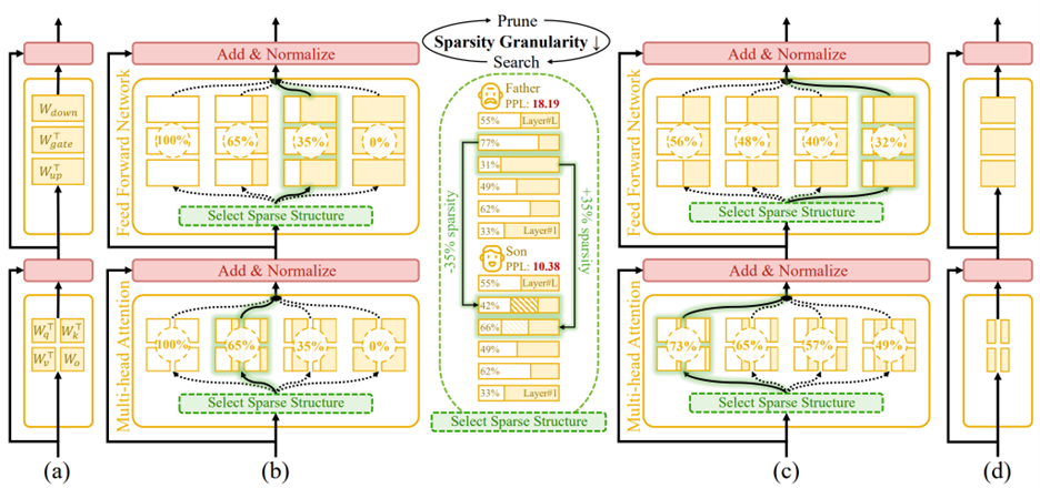
Figure 1. An overview of Týr-the-Pruner. Large language models (a) will be effectively locally pruned across multiple sparsity ratios and constructed into a supernet (b). An iterative prune-and-search strategy will be used to select the optimal sparse structure for each layer while maintaining a target overall sparsity ratio: pruning and sparsity-shift-driven evolutionary search are implemented iteratively with a coarse-to-fine sparsity interval granularity (c). Ultimately, the post-pruned LLM with the optimal sparsity distribution (d) is obtained.
Building a Reliable Supernet
The process begins by locally pruning every layer across multiple sparsity levels. Týr employs Taylor-informed saliency (first- and second-order) alongside backprop-free weight adjustment, applied progressively to minimise performance perturbations.
To ensure that different pruned variants remain mutually consistent, the framework introduces expectation-aware error accumulation, addressing the otherwise ambiguous error propagation that arises when multiple pruned copies coexist within a supernet.
Coarse-to-Fine Global Search
Once the supernet is established, Týr performs an evolutionary sparsity-shift search. Each mutation preserves the global sparsity budget—for example, making one layer slightly denser while another becomes equivalently sparser. Candidate models are evaluated using distillation-based similarity metrics over hidden activations and logits.
A naïve fine-grained search would be intractable: for an 80-sublayer model, even modest sparsity resolution would imply an astronomically large configuration space. Týr sidesteps this with an iterative coarse-to-fine strategy:
- The search begins with a coarse sparsity interval (12.5%) and just nine candidates per layer.
- After identifying a strong sparsity pattern, the search recentres and halves the interval (12.5% → 6.25% → 3.13% → 1.56%).
- After four iterations, Týr reaches fine-grained sparsity resolution while keeping each iteration’s effective search space manageable.
This design steadily narrows the search, accelerates convergence, and efficiently uncovers the optimal global sparsity distribution.
Results: Accuracy and efficiency on AMD hardware
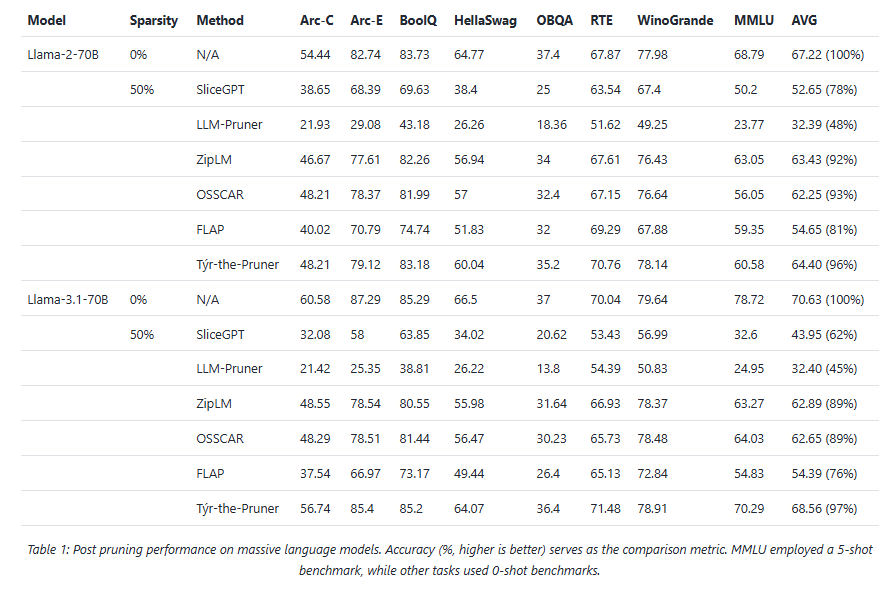
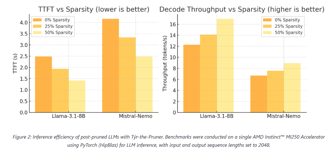
Across models and benchmarks, Týr-the-Pruner consistently preserves near-dense accuracy while delivering meaningful efficiency gains on AMD Instinct MI250 accelerators.
At 50% sparsity, the method retains 96–97% average accuracy on 70B-scale models—outperforming structured pruning approaches such as SliceGPT, LLM-Pruner, and FLAP. On smaller models, the runtime benefits are equally compelling: for Llama-3.1-8B and Mistral-Nemo, pruning cuts time-to-first-token by up to 1.75× and boosts decode throughput by up to 1.38×.
These results position pruning as a first-class optimisation technique for large-scale LLM inference, particularly on modern accelerator architectures.
Practical Considerations: Memory and Search Efficiency
While supernets can be large, Týr keeps memory usage close to that of a single dense model by storing pruned substructures on disk and loading only the active subnet into high-bandwidth memory. Disk footprints remain manageable—around 40 GB for 7–8B models and ~415 GB for 70B models—with older artefacts cleaned up between iterations.
The evolutionary search itself is computationally efficient. Evaluations proceed under progressively increasing token budgets (2K → 16K → 128K), converging rapidly thanks to the coarse-to-fine schedule. For 8B-scale models, a single search iteration completes in a few hours, keeping overall runtime well within practical limits.
Summary
Týr-the-Pruner represents a shift in how global structural pruning is approached. By unifying pruning and sparsity allocation into a single, end-to-end search process—and combining it with expectation-aware error modelling and coarse-to-fine optimisation—the framework achieves both high accuracy retention and real-world inference acceleration.
With up to 50% parameter reduction and ~97% accuracy preserved on Llama-3.1-70B, Týr-the-Pruner demonstrates that global pruning can be both principled and practical—setting a new benchmark for structured pruning in the era of large-scale LLM deployment.
The post Týr-the-Pruner: Search-based Global Structural Pruning for LLMs appeared first on ELE Times.
LEDS Manufactured Backwards
 | My college Electronics class final was to simply solder on parts of a pre-made circuit, and in my case it was an LED Christmas Tree. After soldering 36 TINY AS HELL LEDS, I tested it and there was no lights turning on…. Decided to test an extra LED and turns out the legs were manufactured with the long leg as the negative side and the short leg as the positive side. I’m so cooked [link] [comments] |
Pages

