
Feed aggregator
The role of AI processor architecture in power consumption efficiency

From 2005 to 2017—the pre-AI era—the electricity flowing into U.S. data centers remained remarkably stable. This was true despite the explosive demand for cloud-based services. Social networks such as Facebook, Netflix, real-time collaboration tools, online commerce, and the mobile-app ecosystem all grew at unprecedented rates. Yet continual improvements in server efficiency kept total energy consumption essentially flat.
In 2017, AI deeply altered this course. The escalating adoption of deep learning triggered a shift in data-center design. Facilities began filling with power-hungry accelerators, mainly GPUs, for their ability to crank through massive tensor operations at extraordinary speed. As AI training and inference workloads proliferated across industries, energy demand surged.
By 2023, U.S. data centers had doubled their electricity consumption relative to a decade earlier with an estimated 4.4% of all U.S. electricity now feeding data-center racks, cooling systems, and power-delivery infrastructure.
According to the Berkeley Lab report, data-center load growth has tripled over the past decade and is projected to double or triple again by 2028. The report estimates that AI workloads alone could by that time consume as much electricity annually as 22% of all U.S. households—a scale comparable to powering tens of millions of homes.

Total U.S. data-center electricity consumption increased ten-fold from 2014 through 2028. Source: 2024 U.S. Data Center Energy Usage Report, Berkeley Lab
This trajectory raises a question: What makes modern AI processors so energy-intensive? Whether rooted in semiconductor physics, parallel-compute structures, memory-bandwidth bottlenecks, or data-movement inefficiencies, understanding the causes becomes a priority. Analyzing the architectural foundations of today’s AI hardware may lead to corrective strategies to ensure that computational progress does not come at the expense of unsustainable energy demand.
What’s driving energy consumption in AI processors
Unlike traditional software systems—where instructions execute in a largely sequential fashion, one clock cycle and one control-flow branch at a time—large language models (LLMs) demand massively parallel elaboration of multiple-dimensional tensors. Matrices many gigabytes in size must be fetched from memory, multiplied, accumulated, and written back at amazing rates. In state-of-the-art models, this process encompasses hundreds of billions to trillions of parameters, each of which must be evaluated repeatedly during training.
Training models at this scale require feeding enormous datasets through racks of GPU servers running continuously for weeks or even months. While the computational intensity is extreme, so is the energy footprint. For example, the training run for OpenAI’s GPT-4 is estimated to have consumed around 50 gigawatt-hours of electricity. That’s roughly equivalent to powering the entire city of San Francisco for three days.
This immense front-loaded investment in energy and capital defines the economic model of leading-edge AI. Model developers must absorb stunning training costs upfront, hoping to recover them later through the widespread use of the inferred model.
Profitability hinges on the efficiency of inference, the phase during which users interact with the model to generate answers, summaries, images, or decisions. “For any company to make money out of a model—that only happens on inference,” notes Esha Choukse, a Microsoft Azure researcher who investigates methods for improving the efficiency of large-scale AI inference systems. His quote appeared in the May 20, 2025, MIT Technology Review article “We did the math on AI’s energy footprint. Here’s the story you haven’t heard.”
Indeed, experts across the industry consistently emphasize that inference not training is becoming the dominant driver of AI’s total energy consumption. This shift is driven by the proliferation of real-time AI services—millions of daily chat sessions, continuous content generation pipelines, AI copilots embedded into productivity tools, and ever-expanding recommender and ranking systems. Together, these workloads operate around the clock, in every region, across thousands of data centers.
As a result, it’s now estimated that 80–90% of all compute cycles serve AI inference. As models continue to grow, user demand accelerates, and applications diversify, further widening this imbalance. The challenge is no longer merely reducing the cost of training but fundamentally rethinking the processor architectures and memory systems that underpin inference at scale.
Deep dive into semiconductor engineering
Understanding energy consumption in modern AI processors requires examining two fundamental factors: data processing and data movement. In simple terms, this is the difference between computing data and transporting data across a chip and its surrounding memory hierarchy.
At first glance, the computational side seems conceptually straightforward. In any AI accelerator, sizeable arrays of digital logic—multipliers, adders, accumulators, activation units—are orchestrated to execute quadrillions of operations per second. Peak theoretical performance is now measured in petaFLOPS with major vendors pushing toward exaFLOP-class systems for AI training.
However, the true engineering challenge lies elsewhere. The overwhelming contributor to energy consumption is not arithmetic—it is the movement of data. Every time a processor must fetch a tensor from cache or DRAM, shuffle activations between compute clusters, or synchronize gradients across devices, it expends orders of magnitude more energy than performing the underlying math.
A foundational 2014 analysis by Professor Mark Horowitz at Stanford University quantified this imbalance with remarkable clarity. Basic Boolean operations require only tiny amounts of energy—on the order of picojoules (pJ). A 32-bit integer addition consumes roughly 0.1 pJ, while a 32-bit multiplication uses approximately 3 pJ.
By contrast, memory operations are dramatically more energy hungry. Reading or writing a single bit in a register costs around 6 pJ, and accessing 64 bits from DRAM can require roughly 2 nJ. This represents nearly a 10,000× energy differential between simple computation and off-chip memory access.
This discrepancy grows even more pronounced at scale. The deeper a memory request must travel—from L1 cache to L2, from L2 to L3, from L3 to high-bandwidth memory (HBM), and finally out to DRAM—the higher the energy cost per bit. For AI workloads, which depend on massive, bandwidth-intensive layers of tensor multiplications, the cumulative energy consumed by memory traffic considerably outstrips the energy spent on arithmetic.
In the transition from traditional, sequential instruction processing to today’s highly parallel, memory-dominated tensor operations, data movement—not computation—has emerged as the principal driver of power consumption in AI processors. This single fact shapes nearly every architectural decision in modern AI hardware, from enormous on-package HBM stacks to complex interconnect fabrics like NVLink, Infinity Fabric, and PCIe Gen5/Gen6.
Today’s computing horsepower: CPUs vs. GPUs
To gauge how these engineering principles affect real hardware, consider the two dominant processor classes in modern computing:
- CPUs, the long-standing general-purpose engines of software execution
- GPUs, the massively parallel accelerators that dominate AI training and inference today
A flagship CPU such as AMD’s Ryzen Threadripper PRO 9995WX (96 cores, 192 threads) consumes roughly 350 W under full load. These chips are engineered for versatility—branching logic, cache coherence, system-level control—not raw tensor throughput.
AI processors, in contrast, are in a different league. Nvidia’s latest B300 accelerator draws around 1.4 kW on its own. A full Nvidia DGX B300 rack unit, housing eight accelerators plus supporting infrastructure, can reach 14 kW. Even in the most favorable comparison, this represents a 4× increase in power consumption per chip—and when comparing full server configurations, the gap can expand to 40× or more.
Crucially, these raw power numbers are only part of the story. The dramatic increases in energy usage are multiplied by AI deployments in data centers where tens of thousands of such GPUs are running around the clock.
Yet hidden beneath these amazing numbers lies an even more consequential industry truth, rarely discussed in public and almost never disclosed by vendors.
The well-kept industry secret
To the best of my knowledge, no major GPU or AI accelerator vendor publishes the delivered compute efficiency of their processors defined as the ratio of actual throughput achieved during AI workloads to the chip’s theoretical peak FLOPS.
Vendors justify this absence by noting that efficiency depends heavily on the software workload; memory access patterns, model architecture, batch size, parallelization strategy, and kernel implementation can all impact utilization. This is true, and LLMs place extreme demands on memory bandwidth causing utilization to drop substantially.
Even acknowledging these complexities, vendors still refrain from providing any range, estimate, or context for typical real-world efficiency. The result is a landscape where theoretical performance is touted loudly, while effective performance remains opaque.
The reality, widely understood among system architects but seldom stated plainly is simple: “Modern GPUs deliver surprisingly low real-world utilization for AI workloads—often well below 10%.”
A processor advertised at 1 petaFLOP of peak AI compute may deliver only ~100 teraFLOPS of effective throughput when running a frontier-scale model such as GPT-4. The remaining 900 teraFLOPS are not simply unused—they are dissipated as heat requiring extensive cooling systems that further compound total energy consumption.
In effect, much of the silicon in today’s AI processors is idle most of the time, stalled on memory dependencies, synchronization barriers, or bandwidth bottlenecks rather than constrained by arithmetic capability.
This structural inefficiency is the direct consequence of the imbalance described earlier: arithmetic is cheap, but data movement is extraordinarily expensive. As models grow and memory footprints balloon, this imbalance worsens.
Without a fundamental rethinking of processor architecture—and especially of the memory hierarchy—the energy profile of AI systems will continue to scale unsustainably.
Rethinking AI processors
The implications of this analysis point to a clear conclusion: the architecture of AI processors must be fundamentally rethought. CPUs and GPUs each excel in their respective domains—CPUs in general-purpose control-heavy computation, GPUs in massively parallel numeric workloads. Neither was designed for the unprecedented data-movement demands imposed by modern large-scale AI.
Hierarchical memory caches, the cornerstone of traditional CPU design, were originally engineered as layers to mask the latency gap between fast compute units and slow external memory. They were never intended to support the terabyte-scale tensor operations that dominate today’s AI workloads.
GPUs inherited versions of these cache hierarchies and paired them with extremely wide compute arrays, but the underlying architectural mismatch remains. The compute units can generate far more demand for data than any cache hierarchy can realistically supply.
As a result, even the most advanced AI accelerators operate at embarrassingly low utilization. Their theoretical petaFLOP capabilities remain mostly unrealized—not because the math is difficult, but because the data simply cannot be delivered fast enough or close enough to the compute units.
What is required is not another incremental patch layered atop conventional designs. Instead, a new class of AI-oriented processor architecture must emerge, one that treats data movement as the primary design constraint rather than an afterthought. Such architecture must be built around the recognition that computation is cheap, but data movement is expensive by orders of magnitude.
Processors of the future will not be defined by the size of their multiplier arrays or peak FLOPS ratings, but by the efficiency of their data pathways.
Lauro Rizzatti is a business advisor at VSORA, a company offering silicon solutions for AI inference. He is a verification consultant and industry expert on hardware emulation.
Related Content
- Solving AI’s Power Struggle
- The Challenges of Powering Big AI Chips
- AI Power and Cooling Spawn Forecasting Frenzy
- Benchmarking AI Processors: Measuring What Matters
- Breaking Through Memory Bottlenecks: The Next Frontier for AI Performance
The post The role of AI processor architecture in power consumption efficiency appeared first on EDN.
Created a parallel serial adapter for a dot matrix printer
 | Went to a local electronics store to buy some knobs and things, I mentioned dot matrix printers to an employee and he pulled one out of his butt (the back of the store) and gave it to me for free! Felt like I had to make the serial connector myself to go with the retro feel, so I did! [link] [comments] |
Advancing Quantum Computing R&D through Simulation
Courtesy: Synopsys
Even as we push forward into new frontiers of technological innovation, researchers are revisiting some of the most fundamental ideas in the history of computing.
Alan Turing began theorizing the potential capabilities of digital computers in the late 1930s, initially exploring computation and later the possibility of modeling natural processes. By the 1950s, he noted that simulating quantum phenomena, though theoretically possible, would demand resources far beyond practical limits — even with future advances.
These were the initial seeds of what we now call quantum computing. And the challenge of simulating quantum systems with classical computers eventually led to new explorations of whether it would be possible to create computers based on quantum mechanics itself.
For decades, these investigations were confined within the realms of theoretical physics and abstract mathematics — an ambitious idea explored mostly on chalkboards and in scholarly journals. But today, quantum computing R&D is rapidly shifting to a new area of focus: engineering.
Physics research continues, of course, but the questions are evolving. Rather than debating whether quantum computing can outpace classical methods — it can, in principle — scientists and engineers are now focused on making it real: What does it take to build a viable quantum supercomputer?
Theoretical and applied physics alone cannot answer that question, and many practical aspects remain unsettled. What are the optimal materials and physical technologies? What architectures and fabrication methods are needed? And which algorithms and applications will unlock the most potential?
As researchers explore and validate ways to advance quantum computing from speculative science to practical breakthroughs, highly advanced simulation tools — such as those used for chip design — are playing a pivotal role in determining the answers.

Pursuing quantum utility
In many ways, the engineering behind quantum computing presents even more complex challenges than the underlying physics. Generating a limited number of “qubits” — the basic units of information in quantum computing — in a lab is one thing. Building a large-scale, commercially viable quantum supercomputer is quite another.
A comprehensive design must be established. Resource requirements must be determined. The most valuable and feasible applications must be identified. And, ultimately, the toughest question of all must be answered: Will the value generated by the computer outweigh the immense costs of development, maintenance, and operation?
The latest insights were detailed in a recent preprint, “How to Build a Quantum Supercomputer: Scaling from Hundreds to Millions of Qubits, by Mohseni et. al. 2024,” which I helped co-author alongside Synopsys principal engineer John Sorebo and an extended group of research collaborators.
Increasing quantum computing scale and quality
Today’s quantum computing research is driven by fundamental challenges: scaling up the number of qubits, ensuring their reliability, and improving the accuracy of the operations that link them together. The goal is to produce consistent and useful results across not just hundreds, but thousands or even millions of qubits.
The best “modalities” for achieving this are still up for debate. Superconducting circuits, silicon spins, trapped ions, and photonic systems are all being explored (and, in some cases, combined). Each modality brings its own unique hurdles for controlling and measuring qubits effectively.
Numerical simulation tools are essential in these investigations, providing critical insights into how different modalities can withstand noise and scale to accommodate more qubits. These tools include:
- QuantumATK for atomic-scale modeling and material simulations.
- 3D High Frequency Simulation Software (HFSS) for simulating the planar electromagnetic crosstalk between qubits at scale.
- RaptorQu for high-capacity electromagnetic simulation of quantum computing applications.

Advancing quantum computing R&D with numerical simulation
The design of qubit devices — along with their controls and interconnects — blends advanced engineering with quantum physics. Researchers must model phenomena ranging from electron confinement and tunnelling in nanoscale materials to electromagnetic coupling across complex multilayer structures
Many issues that are critical for conventional integrated circuit design and atomic-scale fabrication (such as edge roughness, material inhomogeneity, and phonon effects) must also be confronted when working with quantum devices, where even subtle variations can influence device reliability. Numerical simulation plays a crucial role at every stage, helping teams:
- Explore gate geometries.
- Optimize Josephson junction layouts.
- Analyze crosstalk between qubits and losses in superconducting interconnects.
- Study material interfaces that impact performance.
By accurately capturing both quantum-mechanical behavior and classical electromagnetic effects, simulation tools allow researchers to evaluate design alternatives before fabrication, shorten iteration cycles, and gain deeper insight into how devices operate under realistic conditions.
Advanced numerical simulation tools such as QuantumATK, HFSS, and RaptorQu are transforming how research groups approach computational modeling. Instead of relying on a patchwork of academic codes, teams can now leverage unified environments — with common data models and consistent interfaces — that support a variety of computational methods. These industry-grade platforms:
- Combine reliable yet flexible software architectures with high-performance computational cores optimized for multi-GPU systems, accessible through Python interfaces that enable programmable extensions and custom workflows.
- Support sophisticated automated workflows in which simulations are run iteratively, and subsequent steps adapt dynamically based on intermediate results.
- Leverage machine learning techniques to accelerate repetitive operations and efficiently handle large sets of simulations, enabling scalable, data-driven research.
Simulation tools like QuantumATK, HFSS, and RaptorQu are not just advancing individual research projects — they are accelerating the entire field, enabling researchers to test new ideas and scale quantum architectures more efficiently than ever before. With Ansys now part of Synopsys, we are uniquely positioned to provide end-to-end solutions that address both the design and simulation needs of quantum computing R&D.
Empowering quantum researchers with industry-grade solutions
Despite the progress in quantum computing research, many teams still rely on disjointed, narrowly scoped open-source simulation software. These tools often require significant customization to support specific research needs and generally lack robust support for modern GPU clusters and machine learning-based simulation speedups. As a result, researchers and companies spend substantial effort adapting and maintaining fragmented workflows, which can limit the scale and impact of their numerical simulations.
In contrast, mature, fully supported commercial simulation software that integrates seamlessly with practical workflows and has been extensively validated in semiconductor manufacturing tasks offers a clear advantage. By leveraging such platforms, researchers are freed to focus on qubit device innovation rather than spending time on infrastructure challenges. This also enables the extension of numerical simulation to more complex and larger-scale problems, supporting rapid iteration and deeper insight.
To advance quantum computing from research to commercial reality, the quantum ecosystem needs reliable, comprehensive numerical simulation software — just as the semiconductor industry relies on established solutions from Synopsys today. Robust, scalable simulation platforms are essential not only for individual projects but for the growth and maturation of the entire quantum computing field.
“Successful repeatable tiles with superconducting qubits need to minimize crosstalk between wires, and candidate designs are easier to compare by numerical simulation than in lab experiments,” said Qolab CTO John Martinis, who was recently recognized by the Royal Swedish Academy of Sciences for his groundbreaking work in quantum mechanics. “As part of our collaboration, Synopsys enhanced electromagnetic simulations to handle increasingly complex microwave circuit layouts operating near 0K temperature. Simulating future layouts optimized for quantum error-correcting codes will require scaling up performance using advanced numerical methods, machine learning, and multi-GPU clusters.”
The post Advancing Quantum Computing R&D through Simulation appeared first on ELE Times.
Overcoming BEOL Patterning Challenges at the 3-NM Node
Courtesy: Lam Research
| ● Controlling critical process parameters is key to managing edge placement error (EPE)
● Simulations revealed that only 9.75% of runs met the minimum line CD success criteria |
As the complementary metal-oxide semiconductor (CMOS) area shrinks 50% from one node to the next, interconnect critical dimensions (CD) and pitch (or spacing) are under tight demands.
At the N3 node, where metal pitch dimensions must be at or below 18 nm,1,2 one of main interconnect challenges is securing sufficient process margins for CD and edge placement error (EPE).
- Achieving the CD gratings for future technology nodes requires multi-patterning approaches, such as self-aligned double/quadruple/octuple patterning (SADP/SAQP/SAOP) and multiple litho-etch (LE) patterning, combined with 193i lithography or even EUV lithography.
SEMulator3D virtual fabrication, part of Semiverse Solutions, was used in a Design of Experiments (DOE) to evaluate EPE and demonstrate the ability to successfully pattern an advanced 18- and 16-nm metal pitch (MP) BEOL.
Using a process model, we explored the impact of process variations and patterning sensitivities on EPE variability. The simulation identified significant process parameters and corresponding process windows that need to be controlled for successful EPE control.
Simulation of 18-nm BEOL Process
A self-aligned litho-etch litho-etch (SALELE) scheme with self-aligned blocks was proposed for an 18-nm MP BEOL process flow used at the N3 node. The advantage of this scheme is that no dummy metal is used in the BEOL, which helps reduce parasitic capacitance.
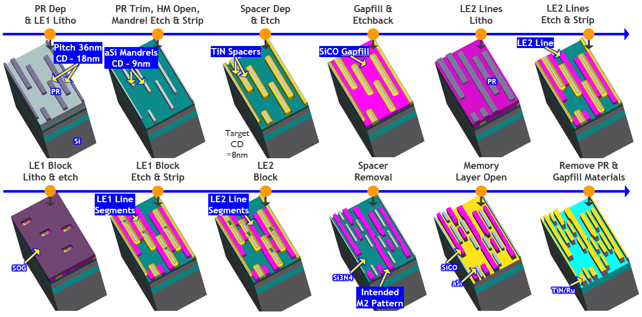
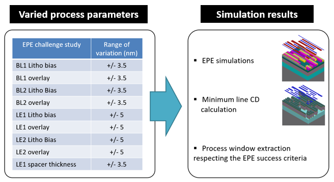
Figure 2 highlights the selected process parameters and corresponding range values used in the DOE simulation. Multiple process parameters that could affect the dimensions of the lines and blocks were varied during simulation using a uniform Monte Carlo distribution.
Parameters such as BL1 Litho bias and LE2 overlay, with range of variation. Simulation results included EPE simulations and Minimum line CD calculation.
In this study, three challenging EPE measurements were evaluated:
- EPE1: EPE calculation of the gap between the printed silicon mandrels for litho etch 1 (LE1) and printed silicon oxycarbide lines for litho etch 2 (LE2)
- EPE2: EPE calculation of the gap between the printed BL1 (block 1) mask after BL1 etch and printed LE1 lines
- EPE3: EPE calculation of the gap between the printed BL2 (block 2) mask after BL2 etch and the printed LE2 lines
Monte Carlo simulations were performed in SEMulator3D across 800 runs using a uniform distribution. For each simulation event, the EPE was extracted using virtual measurements. Process sensitivity analysis was performed in the simulation to investigate the impact of process variations (Figure 2) on the EPE challenges.
The most important process parameters that could impact line dimensions and EPE were automatically identified using the SEMulator3D® Analytics module. Process sensitivity analysis was performed to explore the impact of the most significant parameters on each EPE challenge.
DOE Results
Figure 3 displays an EPE sensitivity analysis plot of EPE1: LE2 on LE1. Spacer thickness defines the gap between the LE2 and LE1 line segments. EPE1 is significantly dependent on spacer thickness variation and less sensitive to LE1 and LE2 litho bias variations.
Three graphs and corresponding virtual representations:-
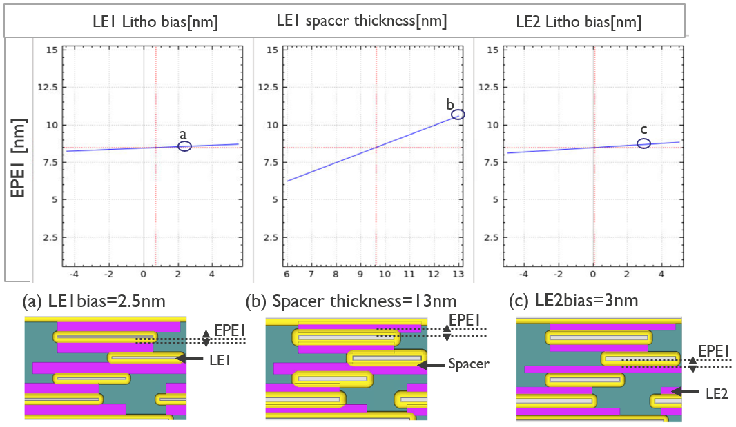
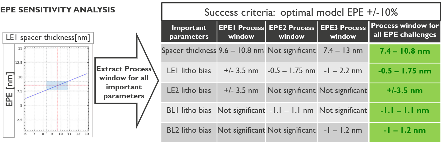
The same EPE sensitivity analysis methodology used in Figure 3 was applied to EPE2 and EPE3. The process sensitivity analysis plots of EPE allowed us to identify acceptable process windows for all three (EPE1, EPE2, and EPE3).
Figure 4 summarizes EPE process windows that were extracted from our process model for the significant process parameters identified earlier.
EPE sensitivity analysis with the extracted process window for all important parameters such as spacer thickness, LE1 litho bias, and BL1 litho bias
Along with evaluating process windows needed to avoid the EPE challenges, minimum line CD was virtually measured for each simulated run. Figure 5 depicts the minimum line CD process window needed to meet the line CD success criteria (8nm<CD<10nm).
Our simulation results indicated that only 9.75% of runs displayed a minimum line CD between 8 and 10 nm. Thus, in addition to the EPE challenge, minimum line CD control is critical and should be considered as part of the process window definition.
Dots on a graph showing a concentration of runs below 10 nm for minimum CD
This study demonstrates that virtual fabrication is a powerful tool for identifying process windows and margins essential for next-generation interconnect technologies. By simulating and analyzing critical process parameters, engineers can proactively address yield-limiting failures and optimize both minimum line CD and EPE control. These insights are vital for advancing semiconductor manufacturing at the 3-nm node and beyond.
The post Overcoming BEOL Patterning Challenges at the 3-NM Node appeared first on ELE Times.
Driving Innovation with High-Performance but Low-Power Multi-Core MCUs
Courtesy: Renesas
Over the last decade, the number of connected Internet of Things (IoT) devices has grown exponentially across markets, ranging from medical devices and smart homes to industrial automation. These smart, connected endpoints implement complex and compute-intensive applications; run real-time control loops; analyze large amounts of data; integrate sophisticated graphics and user interfaces; and run advanced protocols to communicate with the cloud. Machine learning has enabled voice and vision AI capabilities at the edge, empowering devices to make intelligent decisions and trigger actions without cloud intervention. This reduces latency and power consumption, saves bandwidth, and increases privacy. Advanced security has also become an integral part of these systems, as users demand advanced cryptographic accelerators on-chip, robust system isolation, and security for data at rest as well as in motion. Applications also require lower power and fast wake-up times to prolong battery life and reduce overall system power consumption.
These new and emerging requirements drive the need for greater processing power in embedded systems. Fast, reliable, and low-power non-volatile storage of code and data is also needed for the implementation of these sophisticated applications. Traditional systems used either powerful MPUs or multiple MCUs to perform these functions. Recently, we are seeing the emergence of high-performance multi-core MCUs with performance approaching that of MPUs – some with hardware AI accelerators – that can handle all these functions with a single chip. These high-performance MCUs provide a powerful alternative to MPUs for applications where power consumption and cost are critical concerns. MCUs have several advantages over MPUs that make them particularly well-suited for these power-sensitive IoT applications – better real-time performance, integration of power management and non-volatile memory, single voltage rail, lower power, typically lower cost, and ease of use.
The need for higher performance and functionality while keeping power and costs low has driven the movement towards the use of finer process technology nodes like 28nm or 22nm. This movement has driven innovations in embedded memory technology, since embedded flash does not scale well below 40nm. Alternative memory technologies like Magnetoresistive Random Access Memory (MRAM) are being used to replace embedded flash for non-volatile storage. A number of silicon manufacturers like TSMC now provide embedded MRAM that can be integrated into an MCU.
Performance and System Design Flexibility with Dual-Core MCUs
The single-core RA8M2 and RA8D2 MCUs feature the Cortex-M85 core running up to 1GHz, with Helium vector extensions to enable compute-intensive applications. On the dual-core option, a second Cortex-M33 core is added to allow efficient system partitioning, lower power wake-up, and operation. Either core can be configured to be a master or slave CPU and can be independently powered. Inter-processor communication is through flags, interrupts, and message FIFOs.
Dual-core MCUs significantly enhance the performance of IoT applications by enabling greater processing power, efficient task partitioning between the two cores, and improved real-time performance. System tasks can be assigned to different cores, leading to concurrent and more efficient system operation. One core can handle real-time control tasks, sensor interfaces, and communications, while the other, typically a higher-performance core, can handle the compute-intensive tasks, such as execution of neural network model operators, pre-processing of audio or image data, graphics, or motor control. This partitioning between the two cores can enable faster execution and overall improvement in system performance.
With optimal system task partitioning, dual cores can enable lower power consumption. Each core can be independently controlled, allowing them to run at frequencies optimal for the assigned tasks. The lower-performance Cortex-M33 core can be the housekeeping CPU, which enables low-power wake-up and operation. The higher-performance core can stay in low-power mode most of the time to be woken up only when high-performance processing is required. This segregation of tasks with the appropriate use of MCU resources results in overall lower system power consumption.
Dual cores also enable more robust system design. The high-compute tasks can be separated from the more time-critical and safety-critical tasks and real-time control loops, thus allowing a more robust system design. Any interruption on one core will not have an impact on the tasks of the second core. Dual cores can also enable functional safety with core isolation, redundancy, and optimal resource usage by safety-critical and non-critical tasks.
Performance and Power Efficiency with Embedded MRAM
The move to lower process geometries has opened the doors to newer memory alternatives to flash, such as MRAM, which is making its entry into the embedded space as embedded MRAM (eMRAM) and is now included on the RA8M2 and D2 MCUs.
As MCU manufacturers scale to higher performance and functionality with finer process geometries, eMRAM is increasingly being used to replace embedded flash as the non-volatile memory of choice. One key factor that is making MRAM a viable option for use on MCUs is its ability to retain data through solder reflow, which allows the devices to be pre-programmed prior to being soldered on the board. One additional advantage is that MRAM can be used to replace not just the embedded flash (for code) but also SRAM (for data storage) due to the byte addressability (except in cases with security concerns with retention of data across power cycles). Embedded MRAM is now supported by major silicon foundries, which allow MCU manufacturers to incorporate MRAM into new chip designs with minimal cost overhead.
Special care needs to be taken to prevent MRAM from being corrupted by external magnetic fields present in close proximity to the device. MCU manufacturers typically specify magnetic immunity in idle, power off, and operational modes. In order to avoid corruption of MRAM bits, designers will need to provide adequate spacing between an external magnetic field source and the MRAM-based device, so as not to exceed this magnetic immunity specification. Shielding the MRAM with specialized materials is another option to protect the MRAM from a strong magnetic field.
Key Advantages of MRAM Technology:
- True random access non-volatile memory with higher endurance and retention as compared to flash
- Faster write speeds as compared to flash, with no erase needed
- Byte-addressable and simpler to access than flash, similar to SRAM, improving both performance and power
- No leakage when in standby, making them much lower power than SRAM
- Reads are non-destructive and do not need to be refreshed, so it is an alternative to DRAM
- Magnetic layers are not susceptible to radiation, similar to flash
- Fewer mask layers are needed for MRAM as compared to flash, thus lowering costs
- Scales well for lower process technology nodes and, as such, provides a viable alternative to embedded flash
MRAM Applications
MRAM’s low power and non-volatile characteristics make it ideal for various IoT applications as a unified memory, replacing embedded flash, SRAM, or battery-backed SRAM. It can also be used to replace DRAM for data logging applications that require high density, low power, and non-volatile data storage. The immunity to radiation makes it ideal for medical applications in clinical settings and space applications. MRAM can also be used in industrial control and robotics, data center, and smart grid applications, for real-time data storage, fast data retrieval, and replacing battery backup SRAM.
Not forgetting the Edge AI market using machine learning – here, the MRAM can be used to store the AI neural network models and weights, which are retained across power cycles and do not need to be reloaded for execution each time. MRAM, with its fast read/writes, low power, and high endurance, is particularly suited for these applications requiring high processing performance.
In summary, the new and emerging use cases drive the need for high-performance and specialized feature sets on MCUs. Powerful CPU cores, multi-core architecture, new memory technologies like MRAM, and rich peripherals are integrated on RA8M2 and RA8D2 MCUs to support the needs of these cutting-edge applications.
The post Driving Innovation with High-Performance but Low-Power Multi-Core MCUs appeared first on ELE Times.
Evolving from IoT to edge AI system development
Courtesy: Avnet
The advancement of machine learning (ML) along with continued breakthroughs in artificial intelligence (AI) are funnelling billions of dollars into cutting-edge research and advanced computing infrastructure. In this high-stakes atmosphere, embedded developers face challenges with the evolution of Internet of Things (IoT) devices. Teams must now consider how to implement ML and edge AI into IoT systems.
Connected devices at the edge of the network can be divided into two broad categories: gateways and nodes. Gateways (including routers) have significant computing and memory resources, wired power and reliable high-bandwidth connectivity. Edge nodes are much smaller devices with constrained resources. They include smartphones, health wearables, and environmental monitors. These nodes have limited (often battery) power and may have limited or intermittent connectivity. Nodes are often the devices that provide real-time responses to local stimuli.
Most edge AI and ML applications will fall into these two categories. Gateways have the capacity to become more complex, enabled by access to resources such as wired power. What we currently call IoT nodes will also evolve functionally, but are less likely to benefit from more resources. This evolution is inevitable, but it has clear consequences on performance, energy consumption, and, fundamentally, the design.
Is edge AI development more challenging than IoT?
There are parallels between developing IoT devices and adopting edge AI or ML. Both involve devices that will be installed in arbitrary locations and unattended for long periods of time. Data security and the cost of exposure are already key considerations in IoT when handling sensitive information. Edge gateways and nodes retain more sensitive data on-device, but that doesn’t eliminate the need for robust security. Beyond their size and resources, there are significant differences between the two paradigms, as outlined in the table.
Comparing IoT and edge AI applications
| Aspect | IoT Embedded System | Edge AI Embedded System |
| Data Processing | Cloud-based | Local/on-device |
| Intelligence Location | Centralized (cloud/server) | Decentralized (embedded device) |
| Latency | High (depends on network) | Very low/real-time |
| Security Risks | Data exposed in transit | On-device privacy, device-level risks |
| Application Scope | Large networks, basic data | Local analytics, complex inference |
| Hardware Optimization | For connectivity, sensing | For AI model runtime, acceleration |
What’s at stake in edge AI?
IoT devices are data-centric, providing local control along with actionable data that is typically passed to a cloud application. AI and ML at the edge replace cloud dependency with local inferencing. Any AI/ML application starts with sourcing and validating enough data to train a model that can infer meaningful and useful insights.
Once the data is gathered and the source model has been trained, its operation must be optimized through processes such as model pruning, distillation and quantization, to drive simpler inference algorithms on more limited edge AI hardware.
Every time a new set of model parameters is passed to the edge AI device, the investment in training is at risk. Every time an edge node delivers a result based on local inference, it reveals information about the local model. Edge AI devices are also open to physical tampering, as well as adversarial attacks intended to corrupt their operation or even poison the inferencing models they rely upon.
Adaptive models and federated learning
While IoT devices can be maintained using over-the-air (OTA) updates, edge AI systems use adaptive models to adjust their inferencing algorithms and decision-making processes locally in response to external stimuli. This adaptation is valuable because it helps systems deliver resilient performance in evolving situations, such as predictive maintenance for manufacturing processes or patient monitoring in healthcare devices.
Adaptive models also enable edge AI devices to evolve functionally without exposing input data or output decisions. Over time, a source model implemented on an edge AI device should become steadily more valuable as it adapts to real-world stimuli.
This value becomes more apparent when adaptive models are used as part of a federated learning strategy. While edge AI devices using adaptive models keep their learning to themselves, under federated learning strategies, they share.
Each edge AI device adapts its model to better serve its local situation and then, periodically, sends its updated model parameters to the cloud. The submitted parameters are averaged and used to update the source model to reflect this experience. The upside is a source model that is regularly enhanced by field experience from multiple contexts. The challenge is that increasingly valuable model parameters must traverse a network, making them vulnerable to theft or misuse.
Balancing security and model performance
Security measures, such as encryption, help protect model parameters but may be at odds with the design goal of creating a low-resource, highly responsive edge AI device. This challenge can be made more difficult by some strategies used to compress source models to run on low-resource devices.
For example, quantization works by reducing the resolution with which model parameters are expressed, for example, from 32-bit floating-point representations during training to 8- or even 4-bit integers in the compressed version. Pruning disregards nodes whose parameters have a negligible influence on the rest of the model. Distillation implements “teacher–pupil” learning, in which the embedded model learns by relating the inputs and outputs of the source model.
Each of these techniques simplifies the model and makes it more practical for running on resource-constrained hardware, but at the cost of protection against security challenges. For example, quantized or pruned models may offer less redundancy than the source model, making them more efficient, but leave them less resilient to adversarial attacks.
The implementation of security features, such as encrypted parameter storage and communication, or periodic re-authentication, can create processing overheads that undercut the gains achieved by model compression. As the value at risk in edge AI devices rises, embedded engineers will need to weave security concerns more deeply into their development processes. For example, pruning strategies may have to be updated to include “adversarial pruning” in which different parts of a model are removed to see what can be discarded without making the remainder more vulnerable.
Keeping edge AI systems up to date
Embedded edge AI developers will need to be extremely flexible to accommodate rapidly changing ML algorithms, rapidly evolving AI processor options, and the challenge of making the hardware and software work together.
On the hardware side, multiple semiconductor start-ups have been funded to develop edge AI chips. Although the architectures differ, the design goals are often similar:
- Minimize data movement during computation to save power
- Implement extremely efficient arrays of multipliers to do the matrix math involved in ML inference
- Wrap the inferencing engine up in an appropriate set of peripherals for the end application
On the algorithmic side, although ML inferencing involves many standard operations, such as calculating weights and biases in layers or handling back-propagation, the exact way these operations are deployed is evolving rapidly.
Not every combination of ML operations will run well on every processor architecture, especially if the toolchains provided for new chips are immature.
The verification challenge
Design verification may also be a challenge, especially in situations where the implementation of security forces changes to the inferencing models, to the point that they must be retrained, retested and revalidated.
This may be especially important in highly regulated sectors such as healthcare and automotive. Engineers may have to rely heavily on hardware-in-the-loop testing to explore real-world performance metrics such as latency, power, accuracy, and resilience that have been formulated during the development process.
Embedded system designers must be ready to adapt rapidly. Edge AI algorithms, hardware strategies and security issues threatening efficacy are all evolving simultaneously. For edge AI devices, the well-understood challenges of IoT device design will be overlaid with concerns about the value of AI data at rest and on the move.
The impact of security features on inferencing performance must be balanced with the rate of progress in the field. Embedded AI system designers should mitigate these challenges by adhering to standards, choosing established toolchains where possible, and picking well-proven tools to handle issues such as scalable deployment and lifecycle management.
The post Evolving from IoT to edge AI system development appeared first on ELE Times.
From the grid to the gate: Powering the third energy revolution
Courtesy: Texas Instruments
A significant change is unfolding before us. In the 18th and 19th centuries, the Great Britain used coal to power the Industrial Revolution, propelling the transition to machine manufacturing – the first energy revolution. Next, came the second energy revolution, in the United States, where the oil boom of the 20th century fuelled unprecedented advancements in vehicles and electricity.
Today, artificial intelligence (AI) is ushering in the third energy revolution through its rapid growth. Focus is changing on the the generation, conversion, and distribution of the energy needed to power the massive amounts of data we’re consuming. Today, the biggest question is, ‘how to generate the necessary energy required to power data centers and how to efficiently move that energy down the power path – from the grid to the gates of the processors’, which is quickly becoming the most exciting challenge of our times.
Changing distribution levels
As the computing power required by AI data centers scales, data center architectures are undergoing a major change. Typically, servers stack on top of each other in data center computing racks, with power-supply units (PSUs) at the bottom. Alternating current (AC) is distributed to every server rack, where a PSU converts it to 48V and then down to 12V. Point-of-load converters in the server then take it down to the processor gate core voltages.
With the advent of generative AI and the subsequent addition of more servers to process information, racks now need significantly more power. For example, entering a question into a large language model (LLM) requires 10 times the amount of power as entering the same question into a search engine. These increased power levels are pushing power architectures to the limit.

Meeting power demands with solar energy
As data centers require more power to support growing and evolving workloads, renewable energy might just be the answer. Solar is becoming an increasingly viable and affordable energy source in many parts of the world. Coincidentally, data center customers are committing to 100% renewable energy within their companies, and this commitment must be reflected in the data centers they use. Solar can not only help data center customers meet their sustainability goals, but also offers a fast way to deploy more energy generation.
Semiconductors are at the center of the solar power conversion process, making these technologies key to meeting data center power demands. Efficient power conversion and accurate sensing technologies are crucial to making solar a reliable source of energy for the grid.
Energy storage to maximize solar output
Even though data centers operate every hour of every day, solar energy is only available during day time. So how will solar energy help power data centers when the sun isn’t shining? That’s where battery energy storage systems (ESS) become a critical piece of the puzzle, making sure the energy is available and can be used at any time when needed.
Batteries are already an essential component of the grid, effectively storing and releasing large amounts of electricity throughout the grid, and now they’re being used specifically for data centers. Battery management systems within an ESS directly monitor battery cells and assess the amount of energy within, measuring the voltage and determining the state of charge and state of health of the battery to help ensure there is the necessary power available.
In the age of artificial intelligence, data is the new currency, and it’s more valuable than ever. As such, something must power – and sustain – it. We used coal to kickstart factories, and oil to advance automobiles, and now, renewable energy can help us address the growing power needs of data centers in the future.
The post From the grid to the gate: Powering the third energy revolution appeared first on ELE Times.
Rohde & Schwarz India Pvt. Ltd. unveils R&D Centre in New Delhi, India
Rohde & Schwarz announced the expansion of its Research and Development activities in New Delhi, India. This significant move, together with its established facility in Bengaluru, reinforces the company’s commitment to strengthening its presence in the Indian market and underscores its continued focus on innovation and technological advancement. This strategic investment marks a pivotal moment in the company’s commitment to innovation and underscores its dedication to fostering technological advancement within India, directly supporting the nation’s ambitious ‘Make in India’ initiative. The inauguration was presided over by Mr. Andreas Pauly, Chief Technology Officer of Rohde & Schwarz.
Located at Mathura Road, New Delhi, the facility isn’t merely a building; it’s an ecosystem designed to accelerate the development and deployment of next-generation wireless technologies and communications. The R&D Centre is equipped with array of resources, including fully integrated laboratories for complete product lifecycle – from meticulous prototyping, rigorous testing, and comprehensive validation. A dedicated centre, staffed by highly skilled engineers, provides rapid prototyping and debugging capabilities, ensuring swift iteration and accelerating time-to-market.
The core focus of the centre is the development of world-class wireless products leveraging advanced technologies such as 5G New Radio (NR), millimeter wave (mmWave) communications, emerging technologies in satellite communications and 6G. Along with wireless technologies this centre will also host the development of IT applications and secure communication projects. Furthermore, the centre will explore innovative applications of Artificial Intelligence (AI) and Machine Learning (ML) to enhance software development
performance and unlock new possibilities in connected devices.
The post Rohde & Schwarz India Pvt. Ltd. unveils R&D Centre in New Delhi, India appeared first on ELE Times.
Resonant inductors offer a wide inductance range

ITG Electronics launches the RL858583 Series of resonant inductors, delivering a wide inductance range, high current, and high efficiency in a compact DIP package. The family of ferrite-based, high-current inductors target demanding power electronics applications.
 (Source: ITG Electronics)
The RL858583 Series features an inductance range of 6.8 μH to 22.0 μH with a tight 5% tolerance. Custom inductance values are available.
The series supports currents up to 39 A, with approximately 30% roll-off, in a compact 21.5 × 21.0 × 21.5-mm footprint. This provides exceptional current handling in a compact DIP package, ITG said.
Designed for reliability in high-stress operating conditions, the inductors offer a rated voltage of 600 VAC/1,000 VDC and dielectric strength up to 4,500 VDC. The devices feature low DC resistance (DCR) from 3.94 mΩ to 17.40 mΩ and AC resistance (ACR) values from 70 mΩ to 200 mΩ, which helps to minimize power losses and to ensure high efficiency across a range of frequencies. The operating temperature ranges from -55℃ to 130℃.
The combination of high current capability, compact design, and customizable inductance options makes them suited for resonant converters, inverters, and other high-performance power applications, according to ITG Electronics. The RL858583 Series resonant inductors are RoHS-compliant and halogen-free.
The post Resonant inductors offer a wide inductance range appeared first on EDN.
Power resistors handle high-energy pulse applications

Bourns, Inc. releases its Riedon BRF Series of precision power foil resistors for high-energy pulse applications. These power resistors offer power ratings up to 2,500 W and a temperature coefficient of resistance (TCR) as low as ±15 ppm/°C, making them suited as energy dissipation solutions for circuits that require high precision. Applications include current sensing, power management, industrial power control, and energy storage.
 (Source: Bourns, Inc.)
The power resistor series is available in two- and four-terminal options with termination current ratings up to 150 A. This enables developers to tailor the resistors to their exact design requirements, Bourns said.
Other key specifications include a resistance range from 0.001 to 500 Ω, low inductance of <50 nH, and load stability to 0.1%. The operating temperature range is -40°C to 130°C.
The BRF Series of power resistors is built using metal foil technology housed in an aluminum heat sink and a low-profile package. These precision power resistors are designed to meet the rugged and space-constrained requirements of high-energy pulse applications such as power converters, battery energy storage systems, industrial power supplies, inverters, and motor drives.
Available now, the Riedon BRF series is RoHS compliant. Click here for Bourns’ portfolio of metal foil resistors.
The post Power resistors handle high-energy pulse applications appeared first on EDN.
Beneq launches Transform XP second-generation ALD platform
Beneq launches Transform XP second-generation ALD platform
Beneq unveils Transmute high-throughput ALD tool for power, RF and μLED device production
Beneq unveils Transmute high-throughput ALD tool for power, RF and μLED device production
The Linksys MX4200C: A retailer-branded router with memory deficiencies

How timely! My teardown of Linksys’ VLP01 router, submitted in late September, was published one day prior to when I started working on this write-up in late October.

What’s the significance, aside from the chronological cadence? Well, at the end of that earlier piece, I wrote:
There’s another surprise waiting in the wings, but I’ll save that for another teardown another (near-future, I promise) day.
That day is today. And if you’ve already read my earlier piece (which you have, right?), you know that I actually spent the first few hundred words of it talking about a different Linksys router, the LN1301, also known as the MX4300:


I bought a bunch of ‘em on closeout from Woot (yep, the same place that the refurbished VLP01 two-pack came from), and I even asked my wife to pick up one too, with the following rationale:
That’ll give me plenty of units for both my current four-node mesh topology and as-needed spares…and eventually I may decide to throw caution to the wind and redirect one of the spares to a (presumed destructive) teardown, too.
Last month’s bigger brotherHold that thought. Today’s teardown victim was another refurbished Linksys router two-pack from Woot, purchased a few months later, this February to be exact. Woot promotion-titled the product page as a “Linksys AX4200 Velop Mesh Wi-Fi 6 System”, and the specs further indicated that it was a “Linksys MX8400-RM2 AX4200 Velop Mesh Wi-Fi 6 Router System 2-Pack”. It cost me $19.99 plus tax (with free shipping) after another $5 promotion-code discount, and I figured that, as with the two-VLP01 kit, I’d tear down one of the two routers for your enjoyment and hold onto the other for use as a mesh node. Here’s its stock image on Woot’s website:

Looks kinda like the MX4300, doesn’t it? I admittedly didn’t initially notice the physical similarity, in part because of the MX8400 product name replicated on the outer box label:

When I started working on the sticker holding the lid in place, I noticed a corner of a piece of literature sticking out, which turned out to be the warranty brochure. Nice packing job, Linksys!


Lifting the lid:

You’ll find both routers inside, along with two Ethernet cable strands rattling around loose. Underneath the thick blue cardstock piece labeled “Setup Guide” to the right:

are the two power supplies, along with…umm…the setup guide plus a support document:


Some shots of the wall wart follow:


including the specs:

and finally, our patient, as usual, accompanied by a 0.75″ (19.1 mm) diameter U.S. penny for size comparison purposes. Front view:

left side:

back, both an overview and a closeup of the various connectors: power, WAN, three LAN, and USB-A. Hmm…where have I seen that combo before?


right side:

top, complete with the status LED:

and…wait. What’s this?

In addition to the always-informative K7S-03580 FCC ID, check out that MX4200C product name. When I saw it, I realized two key things:
- Linksys was playing a similar naming game to what they’d done with the VLP01. Quoting from my earlier teardown: “…an outer box shot of what I got…which, I’ve just noticed, claims that it’s an AC2400 configuration
 (I’m guessing this is because Linksys is mesh-adding the two devices’ theoretical peak bandwidths together? Lame, Linksys, lame…)” This time, they seemingly added the numbers in the two MX4200 device names together to come up with the “bigger is better” MX8400 moniker.
 - The MX4200(C, in this case) is mighty close to MX4300. Now also realizing the physical similarity, I suspected I had a near-clone (and much less expensive, not to mention more widely available) sibling to the no-longer-available router I’d discussed a month earlier, which, being rare, I was therefore so reticent to (presumably destructively) disassemble.
Some background from my online research before proceeding:
- The MX4200 came in two generational versions, both of them integrating 512 Mbytes of flash memory for firmware storage. V1 of the MX4200 included 512 Mbytes of RAM and had dimensions of 18.5cm (7.3 inches) high and 7.9cm (3.1 inches) wide. The larger, 24.3cm (9.57 inches) high and 11cm (4.45 inches) wide, V2 MX4200 also doubled the internal RAM capacity to 1 GByte.
- This MX4200C is supposedly a Costco-only variant (meaning what beyond the custom bottom sticker? Dunno), conceptually reminiscent of the Walmart-only VLP01 I’d taken apart last month. I can’t find any specs on it, but given its dimensional commonality with the V2 MX4200, I’ll be curious to peer inside and see if it embeds 1 GByte of RAM, too.
- And the MX4300? It’s also dimensionally reminiscent of the V2 MX4200. But this time, there are 2 GBytes of RAM inside it. Last month, I’d mentioned that the MX4300 also bumps up the flash memory to 1 GByte, but the online source I’d gotten that info from was apparently incorrect. It’s 512 GBytes, the same as in versions of the MX4200.
Clearly, now that I’m aware of the commonality between this MX4200C and the MX4300, I’m going to be more careful (but still comprehensive) than I might otherwise be with my dissection, in the hope of a subsequent full resurrection. To wit, here we go, following the same initial steps I used for the much smaller VLP01 a month ago. The only top groove I was able to punch through was the back edge, and even then, I had to switch to a flat-head screwdriver to make tangible disassembly progress (without permanently creasing the spudger blade in the process):


Voila:


Next to go, again as before, are those four screws:


And now for a notable deviation from last month’s disassembly scheme. That time, there were also screws under the bottom rubber “feet” that needed to be removed before I could gain access to the insides. This time, conversely, when I picked up the assembly in preparation for turning it upside-down…


Alrighty, then!


Behold our first glimpses of the insides. Referencing the earlier outer case equivalents (with the qualifier that, visually obviously, the PCB is installed diagonally), here’s the front:

Left side:

Back, along with another accompanying connectors closeup (note, by the way, the two screws at the bottom of the exposed portion of the PCB):


And right side:

Let’s next get rid of the plastic shield around the connectors, which, as was the case last month, lifted away straightaway:


And next, the finned heatsink to its left (in the earlier photo) and the rear right half of the assemblage (when viewed from the front):


We have liftoff:


Oh, goodie, Faraday cages! Hold that thought:

Rotating the assemblage around exposes the other (front left) half and its metal plate, which, with the just-seen four heatsink screws also no longer holding it in place, lifts right off as well:


You probably already noticed the colored wires in the prior shots. Here are the up-top antennas and LED assembly where they end up:


And here’s where at least some of them originate:


Unhooking the wire harness running up the side of the assemblage, along with removing the two screws noted earlier at the bottom of the PCB, enables the board’s subsequent release:

Here’s what I’m calling the PCB backside (formerly in the rear right region) which the finned heatsink previously partially covered and which you’ve already seen:

And here’s the newly-exposed-to-view frontside (formerly front left, to be precise), with even more Faraday cages awaiting my pry-off attention:

I’m happy to oblige. Upper left corner first:

Temporarily (because, as previously mentioned, I aspire to put everything back together in functionally resurrected form later) bend the tab away, and with thanks to Google Image search results for the tip, a Silicon Labs EFR32MG21 Series 2 Multiprotocol Wireless SoC, supporting Bluetooth, Thread, and Zigbee mesh protocols, comes into view. The previously shown single-lead antenna connection on the other side of the PCB is presumably associated with it:

To its left, uncaged, is a Fidelix FMND4G08S3J-ID 512 Mbyte NAND flash memory, presumably for holding the system firmware.
Most of the rest of the cages’ contents are bland, unless you’re into lots of passives; as you’ll soon see, their associated ICs on the other side are more exciting:


Note in all these so-far cases, as well as the remainder, that thermal tape is employed for heat transfer purposes, not paste. Linksys’ decision not only makes it easier to see what’s underneath it will also increase the subsequent likelihood of tape-back-in-place reassembly functional success:


And after all those passives, the final cage at bottom left ended up being IC-inclusive again, this time containing a Qualcomm PMP8074 power management controller:

Now for a revisit of the other side of the PCB, starting with the top-most cage and working our way to the bottom. The first one, with two antenna connectors notably above it, encompasses a portion of the wireless networking subsystem and is based on two Qualcomm Wi-Fi SoCs, the QCN5024 for 2.4 GHz and QCN5054 for 5 GHz. Above the former are two Skyworks SKY85340-11 front-end modules (FEMs); the latter is topped off by two Skyworks SKY85755-11s:


The next cage is for the processor, a quad-core 1.4 GHz Qualcomm IPQ8174, the same SoC and speed bin as in the Linksys MX4300 I discussed last month, and the volatile memory, two ESMT M15T2G16128A 2 Gbit DDR3-933 SDRAMs. I guess we now know how the MX4200C differs from the V2 MX4200; Linksys halved the RAM to 512 GBytes total, reminiscent of the V1 MX4200’s allocation, to come up with this Costco-special product spin.


The third one, this time with four antennae connectors below it, houses the remainder of the (5 GHz-only, in this case) Wi-Fi subsystem; four more Qualcomm QCN5054s, each with a mated Skyworks SKY85755-11 FEM:


And last but not least, at bottom right is the final cage, containing a Qualcomm QCA8075 five-port 10/100/1000 Mbps Ethernet transceiver, only four ports’ worth of which are seemingly leveraged in this design (one WAN, three LAN, if you’ll recall from earlier). Its function is unsurprising given its layout proximity to the two Botthand LG2P109RN dual-port magnetic transformers to its right:


And with that, I’ll wrap up for today. More info on the MX4200 (V1, to be precise) can be found at WikiDevi. Over to you for your thoughts in the comments!
—Brian Dipert is the Principal at Sierra Media and a former technical editor at EDN Magazine, where he still regularly contributes as a freelancer.
Related Content
- A fresh gander at a mesh router
- The pros and cons of mesh networking
- Teardown: The router that took down my wireless network
- Is it time to upgrade to mesh networking?
The post The Linksys MX4200C: A retailer-branded router with memory deficiencies appeared first on EDN.
STMicroelectronics launches GaNSPIN system-in-package family
Understand quadrature encoders with a quick technical recap

An unexpected revisit to my earlier post on mouse encoder hacking sparked a timely opportunity to reexamine quadrature encoders, this time with a clearer lens and a more targeted focus on their signal dynamics and practical integration. So, let’s get a fresh restart and dive straight into the quadrature signal magic.
Starting with a flake of theory, a quadrature signal refers to a pair of sinusoidal waveforms—typically labeled I (in-phase) and Q (quadrature)—that share the same frequency but are offset by 90° in phase. These orthogonal signals do not interfere with each other and together form the foundation for representing complex signals in systems ranging from communications to control.

Figure 1 A visualization illustrates the idealized output from a quadrature encoder, highlighting the phase relationship. Source: Author
In the context of quadrature encoders, the term describes two square wave signals, known as A and B channels, which are also 90° out of phase. This phase offset enables the system to detect the direction of rotation, count discrete steps or pulses for accurate position tracking, and enhance resolution through edge detection techniques.
As you may already be aware, encoders are essential components in motion control systems and are generally classified into two primary types: incremental and absolute. A common configuration within incremental encoders is the quadrature encoder, which uses two output channels offset in phase to detect both direction and position with greater precision, making it ideal for tracking relative motion.
Standard incremental encoders also generate pulses as the shaft rotates, providing movement data; however, they lose positional reference when power is interrupted. In contrast, absolute encoders assign a unique digital code to each shaft position, allowing them to retain exact location information even after a power loss—making them well-suited for applications that demand high reliability and accuracy.
Note that while quadrature encoders are often mentioned alongside incremental and absolute types, they are technically a subtype of incremental encoders rather than a separate category.
Oh, I almost forgot: The Z output of an ABZ incremental encoder plays a crucial role in precision positioning. Unlike the A and B channels, which continuously pulse to indicate movement and direction, the Z channel—also known as the index or marker pulse—triggers just once per revolution.
This single pulse serves as a reference point, especially useful during initialization or calibration, allowing systems to accurately identify a home or zero position. That is to say, the index pulse lets you reset to a known position and count full rotations; it’s handy for multi-turn setups or recovery after power loss.

Figure 2 A sample drawing depicts the encoder signals, with the index pulse clearly marked. Source: Author
Hands-on with a real-world quadrature rotary encoder
A quadrature rotary encoder detects rotation and direction via two offset signals; it’s used in motors, knobs, and machines for fine-tuned control. Below is the circuit diagram of a quadrature encoder I designed for a recent project using a couple of optical sensors.

Figure 3 Circuit diagram shows a simple quadrature encoder setup that employs optical sensors. Source: Author
Before we proceed, it’s worth taking a moment to reflect on a few essential points.
- A rotary encoder is an electromechanical device used to measure the rotational motion of a motor shaft or the position of a dial or knob. It commonly utilizes quadrature encoding, an incremental signaling technique that conveys both positional changes and the direction of rotation. On the other hand, linear encoder measures displacement along a straight path and is commonly used in applications requiring high-precision linear motion.
- Quadrature encoders feature two output channels, typically designated as channel A and channel B. By monitoring the pulse count and identifying which channel leads, the encoder interface can determine both the distance and direction of rotation.
- Many encoders also incorporate a third channel, known as the index channel (or Z channel), which emits a single pulse per full revolution. This pulse serves as a reference point, enabling the system to identify the encoder’s absolute position in addition to its relative movement.
- Each complete cycle of the A and B channels in a quadrature encoder generates square wave signals that are offset by 90 degrees in phase. This cycle produces four distinct signal transitions—A rising, B rising, A falling, and B falling—allowing for higher resolution in position tracking. The direction of rotation is determined by the phase relationship between the channels: if channel A leads channel B, the rotation is typically clockwise; if B leads A, it indicates counterclockwise motion.
- To interpret the pulse data generated by a quadrature encoder, it must be connected to an encoder interface. This interface translates the encoder’s output signals into a series of counts or cycles, which can then be converted into a number of rotations based on the encoder’s cycles per revolution (CPR) counts. Some manufacturers also specify pulses per revolution (PPR), which typically refers to the number of electrical pulses generated on a single channel per full rotation and may differ from CPR depending on the decoding method used.

Figure 4 The above diagram offers a concise summary of quadrature encoding basics. Source: Author
That’s all; now, back to the schematic diagram.
In the previously illustrated quadrature rotary encoder design, transmissive (through-beam) sensors work in tandem with a precisely engineered shaft encoder wheel to detect rotational movement. Once everything is correctly wired and tuned, your quadrature rotary encoder is ready for use. It outputs two phase-shifted signals, enabling direction and speed detection.
In practice, most quadrature encoders rely on one of three sensor technologies: optical, magnetic, or capacitive. Among these, optical encoders are the most commonly used. They operate by utilizing a light source and a photodetector array to detect the passage or reflection of light through an encoder disk.
A note for custom-built encoder wheels: When designing your own encoder wheel, precision is everything. Ensure the slot spacing and width are consistent and suited to your sensor’s resolution requirements. And do not overlook alignment; accurate positioning with the beam path is essential for generating clean, reliable signals.
Layers beneath the spin
So, once again we circled back to quadrature encoders—this time with a bit more intent and (hopefully) a deeper dive. Whether you are just starting to explore them or already knee-deep in decoding signals, it’s clear these seemingly simple components carry a surprising amount of complexity.
From pulse counting and direction sensing to the quirks of noisy environments, there is a whole layer of subtleties that often go unnoticed. And let us be honest—how often do we really consider debounce logic or phase shift errors until they show up mid-debug and throw everything off?
That is the beauty of it: the deeper you dig, the more layers you uncover.
If this stirred up curiosity or left you with more questions than answers, let us keep the momentum going. Share your thoughts, drop your toughest questions, or suggest what you would like to explore next. Whether it’s hardware oddities, decoding strategies, or real-world implementation hacks—we are all here to learn from each other.
Leave a comment below or reach out with your own encoder war stories. The conversation—and the learning—is far from over.
Let us keep pushing the boundaries of what we think we know, together.
 T. K. Hareendran is a self-taught electronics enthusiast with a strong passion for innovative circuit design and hands-on technology. He develops both experimental and practical electronic projects, documenting and sharing his work to support fellow tinkerers and learners. Beyond the workbench, he dedicates time to technical writing and hardware evaluations to contribute meaningfully to the maker community.
Related Content
- Decode a quadrature encoder in software
- Understanding Incremental Encoder Signals
- AVR takes under 1µs to process quadrature encoder
- Linear position sensor/encoder offers analog and digital evaluation
- How to use FPGAs for quadrature encoder-based motor control applications
The post Understand quadrature encoders with a quick technical recap appeared first on EDN.
Rohde & Schwarz presents multi-purpose R&S NGT3600 high-precision dual-channel power supply
Rohde & Schwarz showcases at productronica 2025 the R&S NGT3600 series, a new line of DC power supplies offering up to 1800 W per channel. These power supplies are highly versatile, providing adjustable output voltages of up to 80 V. The two channels of the R&S NGT3622 model can be combined in series or parallel, allowing users to double either the voltage or the current. For applications requiring even more power, up to three units can be connected, delivering up to 480 V or 300 A across six channels.
Exceptionally clean and stable power
The R&S NGT3600 series delivers exceptionally clean and stable power, featuring very low voltage and current ripple and noise. With a resolution of 100 µA for current and 1mV for voltage, the instruments offer precise measurements needed for a wide range of applications.
Adjustable dual-channel power for various test and measurement tasks
The unique two-channel model, the R&S NGT3622, sets a new benchmark for high-performance DC power supplies by combining up to two fully independent 1800 W outputs in a single compact instrument. This represents a significant breakthrough for labs and test systems that demand versatility, space efficiency, and uncompromised precision. Thus, it is ideally suited for measurement and testing tasks in various industries, including power electronics, mobile and satellite communications, renewable energies, automotive, aerospace & defense, among others. The R&S NGT3622 enables precise current and voltage testing under load, efficiency measurements and thermal characterization of components such as DC/DC converters, power supplies, motors, and semiconductors.
Engineers can use a R&S NGT3600 to test high-current prototypes, such as base stations, validate MPPT algorithms for solar inverters, or inspect charging stations. In the automotive sector, it supports the transition to 48 V on-board networks, making it ideal for simulating on-board networks and powering communication systems, sensors, and control units during testing. These capabilities are equally valuable in the aerospace and defense sectors. In short, the R&S NGT3600 is a comprehensive solution for the development and verification of modern DC power supply systems and battery-powered devices.
The post Rohde & Schwarz presents multi-purpose R&S NGT3600 high-precision dual-channel power supply appeared first on ELE Times.
IEEE Wintechon 2025 Powering India’s Semiconductor Future through Data, Diversity and Collaboration
The sixth edition of IEEE WINTECHCON 2025 convened over 800 women engineers, technologists, industry leaders, academia, students, and researchers from November 12 – 13, 2025, under the theme “Transforming the Future with Data-Driven Innovations in the Semicon-Verse.”
Organized by IEEE Bangalore Section, IEEE CAS Bangalore Chapter, and Women in Engineering AG Bangalore Section, the conference was hosted by Samsung Semiconductor India Research (SSIR), this year.
Dr. Chandrakanta Kumar, Chair of the IEEE Bangalore section, said, “IEEE Wintechcon 2025 showcased the strength and momentum of India’s semiconductor innovation engine. The shift toward data-driven and AI-enabled design is redefining what is possible in chip and system development, and this forum brought together the leaders shaping that future. The strong industry and academic participation reflects a clear belief that advancing semiconductor technology demands both technical excellence and inclusive leadership”.
The conference featured keynotes by Jaya Jagadish, Country Head and Senior Vice President of Silicon Design Engineering at AMD; Rajesh Krishnan, Senior Vice President and Managing Director, SSIR; Savithri Seetharaman, Vice President at Texas Instruments; and Sonali Jayswal, Director of System Software at NVIDIA. Garima Srivastava (SSIR) and Puneet Mishra (IEEE) served as the General Chairs for this event.
Rajesh Krishnan, Senior Vice President and Managing Director, SSIR. “Hosting IEEE Wintechcon 2025 was a privilege to showcase the engineering excellence driving the next generation of semiconductor and systems innovation. India stands at a pivotal juncture — with exceptional talent and strong technical rigor, the sector is poised to lead globally. At SSIR, we are advancing this trajectory through cutting-edge R&D, long-term ecosystem partnerships, democratising AI adoption and a focused commitment to nurturing women engineers into technical and product leadership roles that will shape the industry’s future.”
Key takeaways
The two-day program included deep technical sessions across both virtual and in-person formats. Tracks such as “Intelligent Silicon” and “Interstellar Innovations” covered GenAI-powered digital twins, 3D IC integration, advanced packaging, and design-for-test architectures, featuring speakers from Samsung, IBM, Western Digital, Cadence, and Texas Instruments. Day two hosted five parallel paper tracks on AI accelerators, embedded systems, VLSI architectures, and semiconductor packaging, complemented by technology booths, poster sessions, and hands-on demos. A special Masterclass, “From Engineer to Executive,” offered career and leadership insights for emerging women in STEM.
The next edition of IEEE WINTECHCON will be held in November 2026, in Bengaluru, India.
The post IEEE Wintechon 2025 Powering India’s Semiconductor Future through Data, Diversity and Collaboration appeared first on ELE Times.
Pages

