
Feed aggregator
Selective Soldering: Definition, Process, Working, Uses & Advantages
Selective soldering is an advanced soldering technique used in electronics manufacturing to solder specific components on a printed circuit board (PCB) without affecting adjacent parts. Unlike traditional wave soldering, which exposes the entire board to molten solder, selective soldering focuses only on designated areas, making it ideal for complex PCB assemblies with mixed technology components.
This method is essential in industries where high precision and reliability are required, such as aerospace, automotive, medical devices, and telecommunications. Selective soldering helps manufacturers meet stringent quality standards while reducing thermal stress on sensitive components.
How Selective Soldering WorksSelective soldering involves applying molten solder to specific areas of the PCB using a programmable system. It typically follows these key steps:
- Flux Application: A controlled amount of flux is selectively applied to solder joints to improve wetting and prevent oxidation.
- Preheating: The PCB is preheated to activate the flux and reduce thermal shock, ensuring better solder flow.
- Soldering Process: A programmable soldering nozzle or mini-wave applies molten solder to the designated areas, forming high-quality solder joints.
- Cooling and Inspection: The board is cooled down gradually, and automated inspection methods such as X-ray or AOI (Automated Optical Inspection) are used to ensure quality.
The selective soldering process can be categorized into three main techniques:
- Mini-Wave Soldering
This method involves using a small nozzle that creates a miniature solder wave, selectively soldering through-hole components. The PCB moves over the wave, allowing precise solder application.
- Jet Wave Soldering
In this approach, a high-precision nozzle dispenses solder in a controlled manner. It is ideal for densely populated PCBs where precise control is required.
- Laser Selective Soldering
This technique utilizes a laser to heat the solder and create joints without physical contact. It is beneficial for highly sensitive components that require minimal thermal exposure.
Each of these methods is chosen based on factors such as board complexity, component density, and production volume.
Selective Soldering Uses & ApplicationsSelective soldering is widely used across various industries due to its precision and reliability. Some of the primary applications include:
- Automotive Electronics: Used in engine control units (ECUs), infotainment systems, and safety modules where high-reliability soldering is required.
- Aerospace and Defense: Essential for high-reliability PCBs used in avionics and military communication systems.
- Medical Devices: Applied in medical instrumentation where strict quality standards are necessary.
- Consumer Electronics: Used in complex PCB assemblies for smartphones, tablets, and wearables.
- Industrial Automation: Ensures robust connections in industrial control systems and robotics.
- Precision and Selectivity
Selective soldering allows targeted soldering, reducing the risk of damage to nearby components. This is particularly useful for mixed-technology PCBs.
- Reduced Thermal Stress
Unlike wave soldering, which exposes the entire board to heat, selective soldering minimizes thermal exposure, protecting heat-sensitive components.
- Higher Reliability
With precise solder control, the process ensures consistent joint quality, reducing defects such as solder bridges or cold joints.
- Cost-Effectiveness
Selective soldering reduces solder and flux consumption while minimizing rework and scrap rates, leading to cost savings in production.
- Automation Compatibility
Modern selective soldering systems can be fully automated, improving repeatability and efficiency in high-volume manufacturing.
Selective Soldering Disadvantages- Slower Process Compared to Wave Soldering
Since each component is soldered individually, the process is slower than wave soldering, making it less ideal for extremely high-volume production.
- Higher Initial Investment
Selective soldering machines are more expensive compared to traditional soldering equipment, requiring a significant upfront investment.
- Complex Programming and Setup
Proper setup and programming are required to achieve optimal results, necessitating skilled operators and additional setup time.
ConclusionSelective soldering is a vital technique in modern electronics manufacturing, providing high precision, reliability, and cost-efficiency. While it has certain limitations, its advantages make it indispensable for industries requiring robust and precise soldering solutions. As technology advances, selective soldering is expected to become even more efficient, further enhancing its role in electronic assembly processes.
The post Selective Soldering: Definition, Process, Working, Uses & Advantages appeared first on ELE Times.
ams OSRAM’s EVIYOS Shape LED made available
Veeco’s Q4 revenue and income exceed midpoints of guidance
HBM memory and AI processors: Happy together

High-bandwidth memory (HBM) is again in the limelight. At GTC 2025, held in San Jose, California, from 17 to 21 March, SK hynix displayed its 12-high HBM3E devices for artificial intelligence (AI) servers. The Korean memory maker also showcased a model of its 12-high HBM4, currently under development, claiming that it’s now completing the preparatory works for large-scale production of the 12-high HBM4 in the second half of 2025.
Micron, another leading memory supplier, is signaling strong demand for its HBM chips in AI and high-performance computing (HPC) applications. Micron’s chief business officer, Sumit Sadana, told Reuters that all of Micron’s HBM chips are sold out for the calendar year 2025.

Figure 1 HBM is creating a new “near memory” space between cache and main memory. Source: IDTechEx
HBM—essentially a 3D structure of vertically stacked DRAM dies on top of a logic die—relies on advanced packaging technologies like through silicon vias (TSVs) while using a silicon interposer for interconnection with the processor. It’s proving highly suitable in parallel compute environments such as HPC and AI workloads.
That’s because it can handle multiple memory requests simultaneously from various cores in GPUs and AI accelerators to facilitate parallel workload processing. In fact, HBM has become the main venue for overcoming memory bottlenecks in data-intensive HPC and AI workloads. Otherwise, these memory bottlenecks lead to underutilization of AI processors.
What’s also pivotal about HBM devices is their continued development to improve AI accelerator performance. For instance, the current generation HBM3E devices use thermal compression with micro-bumps and underfills to stack DRAM dies. Next, HBM makers like Micron, Samsung and SK hynix are transitioning toward HBM4 devices, which employ advanced packaging technologies such as copper-copper hybrid bonding to increase input/outputs, lower power consumption, improve heat dissipation, and reduce electrode dimensions.
Market research firm IDTechEx’s report “Hardware for HPC, Data Centers, and AI 2025-2035: Technologies, Markets, Forecasts” assesses the key developments and trends in HBM devices serving AI and HPC workloads. It also projects that compared to 2024, the unit sales of HBM are forecast to increase 15-fold by 2035.

Figure 2 The booming AI and HPC hardware is forecast to increase HBM sales 15-fold by 2035. Source: IDTechEx
HBM was a prominent technology highlight in 2024 for its ability to overcome the memory wall for AI processors. With the emergence of HBM4 memory devices, that trend is likely to continue in 2025 and beyond.
Related Content
- HBM Flourishes, But HMC Lives
- AI boom and the politics of HBM memory chips
- Memory Bottlenecks: Overcoming a Common AI Problem
- HBM memory chips: The unsung hero of the AI revolution
- High-bandwidth memory (HBM) options for demanding compute
The post HBM memory and AI processors: Happy together appeared first on EDN.
Cadence Design Centre JV with CSA Catapult backed by £2.5m from Welsh Government
POET ships optical engine samples to three global customers for AI applications
I've been experimenting with making some cross sections over the past week. Here are some of my first attempts
 | The first photo is a cross section from a 12pF 3kV capacitor along it's width. The second photo is that same capacitor along it's length. The third photo is of a 47uF capacitor along it width, but with the layers in the wrong direction giving this damascus like texture. The fourth and fifth photo is this same capacitor along the width (the same orientation as the first photo). Unfortunately, not much can be seen here. I assume that the capacitor plates are too thin and densely packed for my microscope. The sixt photo is of a (pretty bad) crimp terminal. It's just a random terminal I had laying around and I didn't know which cable size and crimping die I had to use for it. The last photo is a cross section of a piece of solder wire, clearly showing its flux core within. I used it to hold the crimped terminal in place while the epoxy was hardening. That's why the crimp terminal can be seen behind it. I still need to get vacuum pump to get rid of the air bubbles, and I also used very cheap epoxy so the clarity of it is not great. But for some first experiments, I think I can call it a success. Next up, I would like to capture some PCB details such as burried and capped via's. [link] [comments] |
Delco Radio 2N278 transistor found at flea market
 | I ran across this today for $5. I believe it is a PNP Germanium power transistor. Along with mica insulators it has a note that looks original. It reads “2N278 transistors are not recommended for replacement in Delco built car radios.” Max Voltage: 45VCEO, 50VCBO. Max Current: 15 Amp. Dissipation: 170 watt. Package: TO-36. That is a lot higher dissipation spec than I expected. [link] [comments] |
Rework
 | My buddy dead bugged a QFN, he is so much more patient than I am. Apparently the engineer connected the belly pad to the wrong voltage [link] [comments] |
Defense industry power supply for testing purposes
 | submitted by /u/Rdp616 [link] [comments] |
Weekly discussion, complaint, and rant thread
Open to anything, including discussions, complaints, and rants.
Sub rules do not apply, so don't bother reporting incivility, off-topic, or spam.
Reddit-wide rules do apply.
To see the newest posts, sort the comments by "new" (instead of "best" or "top").
[link] [comments]
Xor gate
 | But ıt burned because ı forgot to add rezistors a and b [link] [comments] |
Understanding Wire Soldering: Definition, Process, Working, Uses & Advantages
Wire soldering is a fundamental technique in electronics and electrical engineering that involves joining two or more metal wires using a filler metal, known as solder. This process ensures a strong, conductive, and durable connection between components. Soldering is widely used in circuit board assembly, electrical wiring, and microelectronics, offering a reliable means of creating robust electrical and mechanical bonds.
What is Wire Soldering?Wire soldering is a method of joining electrical wires and components by melting a filler metal (solder) at the joint. The solder, typically composed of a lead-tin alloy or a lead-free alternative, melts at a lower temperature than the workpieces, allowing it to flow and solidify, creating a permanent bond. The process ensures excellent electrical conductivity and mechanical strength, making it essential in various industrial and DIY applications.
How Wire Soldering WorksWire soldering works on the principle of wetting and capillary action. Temperature control plays a critical role, as solder melts at specific temperatures, typically 180–200°C for tin-lead solder and 217°C for lead-free solder. Proper heat application ensures strong joints and prevents damage to sensitive electronic components. The use of flux is essential in wire soldering, as it removes oxidation and improves adhesion by enhancing the flow of solder and preventing contaminants from interfering with the bond. Surface preparation is another crucial factor, as clean wire surfaces result in stronger solder joints. Any contaminants like oxidation or dirt can weaken the bond and should be removed before soldering. Additionally, the cooling rate must be managed properly. Gradual cooling prevents joint brittleness and ensures a reliable bond, whereas sudden cooling may introduce stress and weak points in the joint.
Wire Soldering ProcessThe wire soldering process consists of several key steps to ensure a high-quality joint. The first step is preparation, where essential tools such as a soldering iron, solder wire, flux, helping hands or clamps, and wire strippers are gathered. The wire surfaces must be cleaned with alcohol or a wire brush to remove oxidation and dirt, and flux should be applied to improve solder flow and reduce oxidation.
The next step is heating the joint. The soldering iron must be heated to the required temperature, typically between 300–400°C depending on the type of solder being used. The iron tip should be placed in contact with both wires to ensure even heating before applying solder. Once the joint reaches the correct temperature, solder is applied. The molten solder should flow into the joint via capillary action, forming a strong bond. The soldering process should be completed quickly to prevent excessive heat damage to components. The final step is cooling and inspection. The joint must be allowed to cool naturally without disturbance to maintain structural integrity. A visual and mechanical inspection should be performed to ensure proper bonding and electrical continuity.
Wire Soldering Uses & ApplicationsWire soldering finds applications in various industries due to its reliability and efficiency. In the electronics and PCB assembly sector, soldering is used for mounting components on printed circuit boards (PCBs) and is essential in assembling microelectronics and integrated circuits. In the automotive industry, it is widely employed in vehicle wiring, sensors, and electronic control modules, ensuring durable electrical connections resistant to vibrations and environmental stress. The aerospace and defense sectors also rely heavily on wire soldering, particularly in avionics, satellite electronics, and military-grade circuit assemblies. High-reliability soldering techniques are required to withstand extreme environments.
Beyond these industries, wire soldering is commonly used in home electrical repairs, such as fixing household wiring, power cords, and electrical appliances. It provides secure and long-lasting connections in low-voltage circuits. Additionally, industrial manufacturing relies on wire soldering for robotics, automation systems, and power distribution modules, ensuring robust and long-lasting connections for heavy-duty machinery.
Wire Soldering AdvantagesWire soldering offers multiple benefits, making it a preferred method for electrical connections. One of the primary advantages is strong electrical conductivity, as it provides minimal resistance and efficient signal transmission in electronic circuits. It also ensures reliable mechanical strength, offering durable joints that withstand mechanical stress and vibrations. Wire soldering allows for compact and lightweight connections, enabling miniaturization of electronic components, which is ideal for modern gadgets and compact devices. Another key advantage is cost-effectiveness and efficiency, as it requires minimal tools and materials, making it an economical and accessible solution. The process is also quick and versatile, with applications spanning from delicate electronics to heavy-duty electrical work.
Wire Soldering DisadvantagesDespite its advantages, wire soldering has some limitations. One of the main drawbacks is temperature sensitivity. Overheating can damage sensitive components, requiring careful temperature control to avoid such issues. Another potential issue is weak joints. Cold solder joints or insufficient flux application can lead to poor connectivity and reliability problems over time. Additionally, lead-based solder emits toxic fumes, posing health risks. Proper ventilation and safety precautions, such as using fume extractors and protective equipment, are necessary. Lastly, solder joints provide limited structural support. They are not mechanically strong enough for high-load applications and may require additional reinforcement to ensure durability in certain use cases.
ConclusionWire soldering remains an indispensable technique in electronics, automotive, aerospace, and industrial applications. By understanding its principles, process, advantages, and limitations, engineers and technicians can optimize soldering quality for reliable electrical connections. With advancements in lead-free soldering and automated soldering technologies, the future of wire soldering continues to evolve, ensuring improved safety, efficiency, and performance in electrical and electronic manufacturing.
The post Understanding Wire Soldering: Definition, Process, Working, Uses & Advantages appeared first on ELE Times.
Brain-Inspired Neuromorphic Chips Redefining AI Acceleration
Neuromorphic computing represents a groundbreaking paradigm shift in computing, designed to replicate the structure and functionality of biological neural networks. Traditional Von Neumann architectures suffer from inefficiencies due to the separation of memory and processing units, leading to bottlenecks in handling AI and real-time workloads. Neuromorphic chips address these challenges through event-driven computation, parallel processing, and biologically inspired synaptic plasticity. Companies such as Intel, IBM, BrainChip, and SynSense are spearheading the development of these chips, promising enhanced AI acceleration, real-time data processing, and ultra-low power consumption. This article explores the fundamental principles, architectural advancements, diverse applications, industry trends, and future prospects of neuromorphic computing.
Principles of Neuromorphic ComputingNeuromorphic computing is grounded in the principles of spiking neural networks (SNNs) and synaptic plasticity, enabling energy-efficient and event-driven information processing. Unlike traditional deep learning architectures that rely on dense matrix multiplications, SNNs leverage discrete electrical impulses (spikes) for data transmission. This asynchronous operation ensures that computations occur only when necessary, significantly reducing energy consumption. Another core principle is in-memory processing, where neuromorphic chips integrate memory and computation units to eliminate data transfer bottlenecks, a limitation of conventional architectures.
Adaptive learning mechanisms further distinguish neuromorphic chips from traditional AI accelerators. Inspired by Hebbian learning and long-term potentiation, these chips modify synaptic weights dynamically based on data patterns, mirroring human cognitive processes. Additionally, neuromorphic architectures exhibit massive parallelism, as thousands or even millions of artificial neurons and synapses operate simultaneously. This makes them ideal for real-time, low-latency AI inference applications in power-constrained environments such as edge devices and wearables.
Architectures of Neuromorphic ChipsNeuromorphic chip architectures vary widely, encompassing digital, analog, and hybrid designs. Digital neuromorphic processors, such as Intel’s Loihi 2, leverage asynchronous spike-based processing with over one million programmable neurons and hierarchical synaptic plasticity mechanisms. Loihi 2 features optimized learning rules, improved interconnectivity, and enhanced support for complex AI workloads, making it a leading candidate for next-generation AI acceleration.
BrainChip’s Akida platform, another prominent digital neuromorphic processor, is tailored for ultra-low power AI inference at the edge. It employs event-based processing, leveraging hierarchical temporal memory (HTM) principles to achieve highly efficient pattern recognition. The Akida chip is designed to optimize convolutional neural network (CNN) inference while maintaining minimal power consumption, making it suitable for applications such as smart surveillance, autonomous systems, and health monitoring.
Analog and mixed-signal neuromorphic chips offer even greater efficiency by utilizing physical transistor properties to mimic neuronal activity. IBM’s TrueNorth, a hybrid digital-analog neuromorphic system, incorporates one million neurons and 256 million synapses, enabling large-scale SNN processing with extremely low power consumption. Memristor-based neuromorphic architectures, such as those under development at MIT and HP, integrate non-volatile resistive RAM (RRAM) elements to implement synaptic weights directly in hardware, further reducing energy overheads.
Another emerging approach is 3D neuromorphic architectures, where stacked layers of artificial neurons are fabricated to enhance computational density and minimize interconnect delays. Researchers at ETH Zurich and Stanford University are exploring hybrid 3D CMOS-memristor designs to enable brain-scale neuromorphic computing, opening new frontiers in AI efficiency and scalability.
Applications of Neuromorphic ChipsNeuromorphic computing has transformative applications across diverse sectors, revolutionizing AI-driven decision-making, robotics, medical diagnostics, and edge intelligence.
Edge AI and IoT
Neuromorphic chips excel in ultra-low power AI inference, making them ideal for always-on smart sensors, real-time environmental monitoring, and security surveillance. They enable real-time AI processing in IoT devices, allowing predictive maintenance, autonomous energy management, and adaptive user interfaces in smart homes and industrial automation.
Robotics and Autonomous Systems
Neuromorphic processors are redefining robotics by enabling real-time, low-latency decision-making. Their ability to process sensory inputs dynamically makes them well-suited for applications in humanoid robots, collaborative automation, and autonomous vehicles. For instance, neuromorphic vision sensors enhance object detection and navigation by replicating biological vision processing, enabling real-time adaptation in self-driving cars and drones.
Healthcare and Biomedicine
In healthcare, neuromorphic chips power advanced neural interfaces, brain-machine interaction (BMI) systems, and real-time biomedical signal processing. They facilitate ultra-fast EEG and ECG analysis, enabling rapid diagnosis of neurological disorders such as epilepsy and Parkinson’s disease. Additionally, neuromorphic AI enhances medical imaging, assisting in early disease detection with significantly reduced computational overhead.
Cybersecurity and AI at the Edge
The adaptive learning capabilities of neuromorphic chips make them well-suited for AI-driven cybersecurity solutions. Their ability to detect anomalous patterns in real-time enhances intrusion detection systems (IDS) and fraud prevention mechanisms. Moreover, neuromorphic architectures support biometric authentication technologies, such as facial recognition and voice-based identity verification, ensuring energy-efficient, secure access control solutions.
Industry Insights and Market TrendsThe neuromorphic computing landscape is evolving rapidly, with significant investments from semiconductor giants, startups, and government agencies.
Key Players and Research InitiativesIntel has established the Neuromorphic Research Community (INRC) to accelerate the adoption of Loihi-based computing platforms. IBM continues to explore hybrid analog-digital neuromorphic accelerators, while BrainChip expands the Akida ecosystem for low-power AI applications. Emerging startups like SynSense and Innatera are focusing on commercializing neuromorphic AI accelerators for edge computing, demonstrating a growing market appetite for these technologies.
Investment and Commercialization TrendsVenture capital funding for neuromorphic startups has increased, with investors recognizing the potential of brain-inspired computing in AI acceleration and IoT. Government and defense organizations, including DARPA, are investing in neuromorphic architectures for autonomous surveillance systems, next-generation military drones, and AI-powered secure communications. Academia-industry collaborations, particularly in the U.S., Europe, and China, are driving advancements in neuromorphic hardware scalability and software frameworks.
Challenges and OpportunitiesDespite significant progress, neuromorphic computing faces challenges in software compatibility, standardization, and large-scale fabrication. Existing AI frameworks, such as TensorFlow and PyTorch, are not natively optimized for SNNs, necessitating new programming paradigms. Scalability remains a concern, as manufacturing neuromorphic chips with millions of interconnected artificial neurons requires advanced semiconductor fabrication techniques.
Future ProspectsThe next decade will witness the convergence of neuromorphic computing with emerging technologies such as quantum computing, biohybrid systems, and 3D-integrated AI architectures. Quantum neuromorphic computing, which combines quantum-inspired neural networks with spike-based processing, holds promise for solving complex optimization problems with unprecedented efficiency. Furthermore, brain-on-chip innovations, integrating living neuronal cultures with synthetic neural networks, could pave the way for biologically realistic AI models.
As AI workloads become increasingly complex, neuromorphic chips will play a crucial role in advancing edge intelligence, real-time robotics, and human-like cognition in machines. By mimicking the energy efficiency and adaptability of the human brain, neuromorphic architectures are poised to redefine the future of computing, unlocking unparalleled capabilities across diverse technological domains.
The post Brain-Inspired Neuromorphic Chips Redefining AI Acceleration appeared first on ELE Times.
electronica China 2025: High-quality Chinese and International Companies Gather at this Can’t-miss Electronics Event with 100,000 Square Meters
electronica China 2025 will take place from April 15 to 17, 2025 at the Shanghai New International Expo Centre (SNIEC), in halls W3-W5 and N1-N5. It is expected to attract a total of almost 1,800 high-quality exhibitors from domestic and international markets covering 100,000 square meters. Register now and check out the latest updates on the exhibition area!
Click to register now: https://ec.global-eservice.com/?lang=en&channel=enmd
Fairgrounds Map
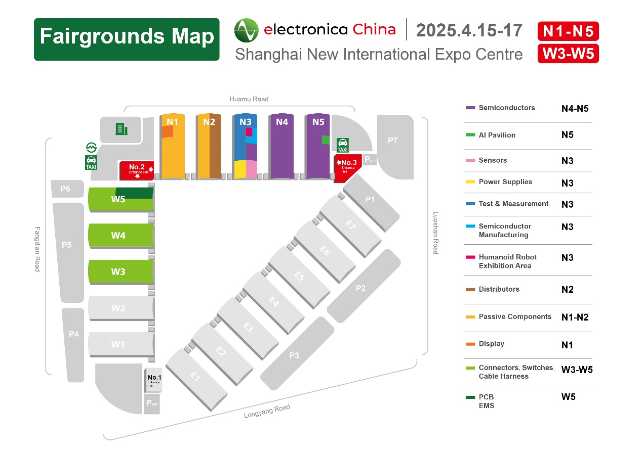
Overview some important exhibition areas
Semiconductors & Sensors
In recent years, the rapid development of the Internet of Things (IoT) industry in China has positioned sensors as one of the core components of the country’s “Strong Foundation Project”. As a result, the market scale and application scenarios for sensors in China have continued to grow. electronica China 2025 will include exhibition areas for semiconductors and sensors, gathering numerous high-quality exhibitors to discuss industry development on-site.
Test and Measurement & Power Supplies
The power supply industry in China has seen rapid growth fueled by international industrial relocation, the ongoing development of China’s information technology, and the continuous advancements in the defense and military sectors. The 2025 exhibition will feature bring together companies to showcase their products and participate in technological discussions in the test and measurement, and power supply exhibition areas.
Connectors, Switches and Cable Harness
In recent years, the connector market has experienced overall growth, fueled by the rapid development of downstream industries such as consumer electronics, new energy vehicles, communications, and industrial control. electronica China 2025 will feature a connector exhibition area, inviting numerous leading exhibitors from the connector industry to showcase their new products.
PCB & EMS
With the maturation of the EMS industry model and ongoing technological advancements and capacity upgrades by companies, the global EMS market is experiencing greater diversity in its downstream customer sectors. At present, EMS is extensively applied across a range of sectors, including consumer electronics, automotive electronics, industrial control electronics, etc. electronica China 2025 will set up PCB and EMS exhibition areas.
Passive Components & Distributors
The development of technologies like 5G communication, artificial intelligence (AI), and the IoT is presenting substantial opportunities for the passive components industry. Additionally, passive components are widely used in such fields as telecommunications, power, automotive electronics, and healthcare, providing substantial growth opportunities for the industry. electronica China 2025 will set up passive components and distributors exhibition areas.
Click to register now: https://ec.global-eservice.com/?lang=en&channel=enmd
Learn more about electronica China: https://www.electronicachina.com.cn/en
The post electronica China 2025: High-quality Chinese and International Companies Gather at this Can’t-miss Electronics Event with 100,000 Square Meters appeared first on ELE Times.
The Inside of an old Leon Paul scoring machine (Olympic fencing)
") | I'm in the process of stripping this old scoring machine down to replace the insides with an Arduino. I think this machine dates back to the 1960s. Interestingly, it only has modes for Épée and foil (no saber), but yeah it is a fairly interesting piece of history. [link] [comments] |
Found 2 Raytheon 7489s (mfd 1973) to repair a Pacman board.
 to repair a Pacman board.") | submitted by /u/weirdal1968 [link] [comments] |
Silicon Austria Labs and TU Graz launch joint Power Electronics Research Laboratory
USPTO gives ruling on EPC patent disputed by Innoscience
Breaking Boundaries with Photonic Chips and Optical Computing
As traditional semiconductor-based computing approaches its physical and energy efficiency limits, photonic chips and optical computing have emerged as transformative solutions. By harnessing the speed and parallelism of light, these technologies offer significant advantages over conventional electronics in high-performance computing (HPC), artificial intelligence (AI), and data centers. Optical computing has the potential to revolutionize the way information is processed, enabling faster, more energy-efficient computation with lower latency.
The Fundamentals of Photonic ChipsPhotonic chips leverage integrated photonics to manipulate light for computing, communication, and sensing applications. Unlike traditional chips that use electrons as the primary carriers of information, photonic chips use photons, which can travel at the speed of light with minimal energy loss. Key components of photonic chips include:
- Waveguides: Optical channels that guide light through a photonic circuit, analogous to electrical traces in traditional chips.
- Modulators: Convert electrical signals into optical signals by modulating light properties such as intensity or phase.
- Detectors: Convert optical signals back into electrical signals for further processing.
- Resonators and Interferometers: Facilitate advanced signal processing functions such as filtering, multiplexing, and logic operations.
- Photonic Crystals: Control the flow of light by creating periodic dielectric structures, enhancing optical confinement and manipulation.
Optical computing aims to replace or supplement electronic computation with light-based logic operations. This transition offers several key advantages:
- Unparalleled Speed: Photons travel at the speed of light, reducing signal delay and increasing processing throughput.
- Low Energy Consumption: Unlike electrical circuits that suffer from resistive heating, photonic systems dissipate minimal heat, enhancing energy efficiency.
- Massive Parallelism: Optical systems can process multiple data streams simultaneously, significantly improving computational throughput.
- Reduced Signal Crosstalk: Optical signals do not experience the same interference as electrical signals, reducing errors and noise in computation.
Silicon photonics integrates optical components onto a silicon platform, enabling compatibility with existing semiconductor fabrication techniques. Key innovations in silicon photonics include:
- On-chip Optical Interconnects: Replace traditional copper interconnects with optical waveguides to reduce power consumption and signal delay.
- Optical RAM and Memory: Photonic memory elements store and retrieve data using light, enhancing data transfer speeds.
- Electro-Optical Modulators: Convert electronic signals to optical signals efficiently, allowing seamless integration into existing computing architectures.
Optical computing relies on photonic logic gates to perform fundamental computations. These gates operate using:
- Nonlinear Optical Effects: Enable all-optical switching without electronic intermediaries.
- Mach-Zehnder Interferometers (MZI): Implement XOR, AND, and OR logic functions using light phase interference.
- Optical Bistability: Maintains state information in optical latches, paving the way for optical flip-flops and memory elements.
With the growing demand for AI processing, photonic neural networks offer an alternative to traditional GPUs and TPUs. Optical deep learning accelerators employ:
- Matrix Multiplication with Light: Perform multiply-accumulate operations at light speed using photonic interference.
- Optical Tensor Processing Units (TPUs): Enhance AI inference by leveraging photonic components for ultra-fast computation.
- Wavelength-Division Multiplexing (WDM): Enables parallel processing by encoding multiple data streams onto different wavelengths of light.
Quantum computing benefits immensely from photonics due to the inherent properties of quantum light. Advancements in quantum photonic processors include:
- Single-Photon Sources and Detectors: Essential for quantum information processing and cryptographic applications.
- Quantum Key Distribution (QKD): Enables ultra-secure communication leveraging the principles of quantum entanglement.
- Optical Quantum Logic Gates: Facilitate complex quantum computations with minimal decoherence.
Modern data centers face thermal constraints and power limitations due to electronic interconnects. Photonic interconnects dramatically reduce power consumption and increase bandwidth, making them an ideal solution for high-speed data transmission between servers and storage units.
2. Artificial Intelligence and Machine Learning AccelerationAI workloads rely on extensive matrix operations, which photonic computing executes at orders of magnitude faster speeds than traditional electronics. Companies like Lightmatter and Lightelligence are pioneering photonic AI accelerators to enhance deep learning performance while reducing energy costs.
3. Telecommunications and Optical NetworksFiber-optic networks already leverage photonics for data transmission, but photonic computing extends these advantages to real-time processing. Photonic switches enable ultra-fast data routing, improving the efficiency of 5G and future 6G networks.
4. Healthcare and BiophotonicsOptical computing is revolutionizing biomedical imaging and diagnostics. Photonic chips enable high-resolution imaging techniques such as optical coherence tomography (OCT) and bio-sensing applications, enhancing early disease detection.
5. Defense and AerospaceThe military and aerospace industries require ultra-fast, secure processing for signal intelligence, radar systems, and cryptographic applications. Optical computing’s speed and resistance to electromagnetic interference make it a critical enabler for next-generation defense systems.
Challenges and Future Roadmap 1. Fabrication Complexity and ScalabilityWhile photonic chips leverage semiconductor manufacturing techniques, integrating large-scale optical circuits remains a challenge. Standardizing fabrication methods and developing CMOS-compatible photonic components are essential for commercial scalability.
2. Hybrid Photonic-Electronic ArchitecturesDespite the advantages of photonic computing, hybrid architectures that integrate both electronic and optical components are likely to dominate in the near term. Developing efficient electro-optic interfaces remains a key research focus.
3. Software and Algorithm DevelopmentCurrent software is optimized for electronic computation, requiring a shift in programming paradigms for photonic systems. Developing photonic-aware compilers and simulation tools will accelerate adoption.
4. Energy Efficiency and Power ConsumptionWhile photonic computing reduces heat dissipation, the challenge lies in optimizing light generation and detection components to minimize power consumption further.
Conclusion: The Dawn of the Photonic Computing EraPhotonic chips and optical computing represent a paradigm shift in computation, offering unparalleled speed, efficiency, and scalability. As silicon photonics, quantum optics, and neuromorphic photonic computing continue to advance, the technology is poised to revolutionize AI, data centers, telecommunications, and beyond. Overcoming fabrication, software, and integration challenges will be crucial for realizing the full potential of photonic computing, marking the beginning of a new era in information processing.
The post Breaking Boundaries with Photonic Chips and Optical Computing appeared first on ELE Times.
Pages


![[link]](https://i.redd.it/ln2yiu2msbqe1.jpeg)
![[link]](https://i.redd.it/4fd9a8m25bqe1.jpeg)
![[link]](https://i.redd.it/jw68cq6li4qe1.jpeg)