


Feed aggregator
Anritsu Chosen by University of Pretoria for Africa’s Only Sub-Terahertz Facility
Anritsu EMEA GmbH has announced that the Carl and Emily Fuchs Institute for Microelectronics (CEFIM) at the University of Pretoria has selected the Anritsu VectorStar Broadband Vector Network Analyzer (VNA) at 220 GHz as the core measurement platform for the only complete sub-terahertz (sub-THz) measurement facility in Africa. By establishing this capability locally, CEFIM will give researchers in South Africa and across the region access to advanced sub-THz measurement resources that previously required facilities overseas.
At the heart of the facility is Anritsu’s VectorStar Broadband VNA, which provides continuous broadband coverage up to 220 GHz. Together with harmonic mixers and calibrated noise analysis capabilities, the system enables the characterization of microwave and millimeter-wave devices operating in the sub-terahertz frequency range.
The installation extends CEFIM’s previous measurement capability from 110 GHz to 220 GHz, giving researchers access to calibrated measurements over a significantly wider frequency range and enabling more complete validation of high-frequency device designs.
Selected for advanced researchThe facility will support a wide range of research activities within CEFIM, including work related to next-generation wireless communications, radio astronomy, water vapor radiometry and other sub-terahertz technologies. It will also support the institute’s participation in international research initiatives, including the African Millimetre Telescope project and the development of receivers for next-generation radio astronomy.
“As an emerging field of research, no facility previously existed in South Africa to measure electromagnetic waves and devices at these frequencies,” said Professor Tinus Stander, Carl and Emily Fuchs Institute for Microelectronics, University of Pretoria. “The establishment of this facility will support research in future wireless communications, radio astronomy and a range of emerging applications that require measurement capabilities well above 100 GHz.”
“Leading research institutions require reliable measurement solutions when they push the boundaries of microwave and millimeter-wave technology. We are proud that CEFIM has chosen Anritsu’s VectorStar Broadband VNA for their facility, and we see this project as a further example of the trust that universities and research organizations place in Anritsu for advanced high-frequency measurements,” said Marco Bordin, Sales Director, Southern Region, Anritsu EMEA.
The facility was established under the National Equipment Programme of South Africa’s National Research Foundation (NRF). The Anritsu solution was supplied in collaboration with Tamashi Technology Investments, Anritsu’s authorized representative in South Africa.
Pictured, among others, are Dr. Heinrich Laue and Professor Tinus Stander (University of Pretoria), Darius Opperman (Tamashi Technology Investments) and Stefano Balzarini (Anritsu).
The post Anritsu Chosen by University of Pretoria for Africa’s Only Sub-Terahertz Facility appeared first on Open Electronics.
HIRO: the educational quadruped robot powered by Raspberry Pi Pico 2
HIRO is a second-generation educational robotics kit shaped like a spider-like quadruped. It is designed by Joseph Casebeer and powered by a Raspberry Pi Pico 2. The kit arrives disassembled: the user assembles it, wires it, and decides which software to run. The project updates the original model with a more powerful board and more durable materials.
The heart of the robot is the Cortex motherboard, which hosts the Raspberry Pi Pico 2. The board features eight connectors for motor control and four mounting points for the included SG-90 servo motors. The robot also integrates a six-axis inertial measurement unit TDK MPU-6050, five photoresistors, five push buttons, ten LEDs, and two piezoelectric buzzers. Assembly takes about 20-30 minutes and also involves the use of a solderless breadboard included in the kit.
Assembly and kit componentsThe kit is designed to be fully customizable. The buyer has full rights to repair and modify it. The stated assembly time is 20-30 minutes, thanks to the solderless breadboard that avoids any soldering work. The main components are as follows:
- Raspberry Pi Pico 2, the microcontroller board
- Cortex motherboard, the central main board
- Eight SG-90 servo motors for the legs
- Six-axis TDK MPU-6050 IMU
- Five photoresistors and five push buttons
- Ten LEDs and two piezoelectric buzzers
The Cortex board manages the motors through its eight dedicated connectors. The four mounting points secure the servo motors to the frame. The MPU-6050 IMU provides orientation and acceleration data, while the photoresistors and push buttons offer input for interacting with the environment. The LEDs and buzzers complete the visual and audible feedback.
Software and Kickstarter campaignThe source code for the robot’s movement library is available on GitHub under the MIT license. This allows anyone to study, modify, and adapt it to their own needs. The project is described as open source, although the hardware design files have not been released. Those who want to dig deeper can check Joseph Casebeer’s funding campaign for full details.
The kit price for first-day backers on Kickstarter is $149. The Cortex board alone costs $60. Hardware shipping is expected for June 2027. The kit is therefore an investment for those who want to learn robotics hands-on, with a project that can be taken apart and reassembled at will.
The post HIRO: the educational quadruped robot powered by Raspberry Pi Pico 2 appeared first on Open Electronics.
How did antennas get so small?

Antennas are among the most “analog” of all components, functioning as bidirectional transducers between ambient RF energy and electrical current flow. For many years, most antennas were physically obvious and visual, ranging from modest whip antennas (formally called a monopole or Marconi) with ground planes used on portable and car radios, to the big dishes used for radio astronomy or radar (Figure 1).
Yes, it’s called an “aerial” in some countries, but we’ll just stick with “antenna” here.

Figure 1 The antenna “family tree” is complicated and somewhat bewildering; this is just one possible version. Source: Pressbooks
Other installations use some variation of the dipole antenna, such as the classic TV “rabbit ears” from the 1950s and 1960s (Figure 2). Regardless of type, antennas made a clear statement: they were tangible, and they were doing critical wireless work.

Figure 2 This dipole antenna, affectionally called a “rabbit ears” antenna, was a standard set-top fixture on analog VHF TVs (the loop antenna is for the added UHF band). Source: Wideskall via Wal-Mart
Now, antennas are often invisible even on products which used to have visible ones. Consider the cell phone and smartphone. I was doing some research into the history of cell phones since the first commercial units—when they were just phones and not “smart” —and one thing struck me: they all had external antennas, about 12 inches (30 cm) long (Figure 3).

Figure 3 The all-analog Motorola DynaTAC 8000x (1983) was the first commercial cell phone. Due to its high price ($3,995 at launch), it also became a status symbol despite its one-hour talk time. Source: PC Magazine
Some were short whips, some were so-called “rubber duckies” where the antenna was wound around a semi-ridged post. For some cell phones, such as the classic Motorola Star-Tac flip phone, the unit would fit in the pocket, but the user had to pull the antenna out of the phone body enclosure to use the phone (Figure 4).

Figure 4 One of the earliest successful cell phones, this Motorola MicroTAC Classic was released in 1991 and supported a single RF band via its extendable whip (monopole) antenna. Source: Southside Allstars
One Dell desktop PC I had about 15 or 20 years ago had an external detachable antenna for Wi-Fi access. While that seemed like a nuisance, it actually was a benefit as it allowed me to use a separate cable-connected antenna from D-Link in its place and locate it to get a better signal (Figure 5). Now, all the desktop PCs that I have checked feature a small permanent antenna on or just inside their case, and no ability to add an antenna (yes, there are various boosters and repeaters to solve the problem, but they are active and require setup).

Figure 5 The ANT700-2400 2.4 GHz Wi-Fi antenna, with supplied cable and connector, allowed me to easily move the antenna from the PC to a better location. Source: D-Link Australia
That was then… “now” is very different
Antenna reality has changed dramatically, even if the basic physics and Maxwell’s equations have not. Smartphones and just about any wireless-connected consumer device—phone, router, smart “whatever”—now implement connectivity with an antenna that is embedded in the unit. This simplifies packing, avoids user breakage, eliminates the need for a discrete antenna connector, and presents a sleeker, more user-friendly product. It’s almost as if a magician stepped in and made the visible antenna disappear right in front of our eyes.
How did effective antennas go from larger external add-ons to tiny internal ones? Part of the reason is the migration to higher frequencies with shorter wavelengths, but that’s only part of it. After all, going from 500 MHz to 1 GHz cuts the wavelength in half, but these internal antennas are far smaller than one-half of those earlier ones.
A large part is due to new material technologies, aided by advanced electromagnetic modeling and simulation.
First, there is the microstrip patch antenna, which uses the PCB copper itself as the antenna and surrounding ground plane. This flat, low-profile antenna is made of a metal patch on one side of the circuit board and a solid metal ground layer on the other.
It’s compact with no direct cost and can even be configured for multi-band performance. However, it occupies PCB real estate and requires careful management of its dimensions as well sufficient ground plane, and may have an unacceptable radiation pattern.
As a result, the simple microstrip antenna may not be a suitable option despite its apparent benefits. For these reasons, patch and other specialty antennas may offer the form factor and specifications needed for an internal antenna.
For example, there’s the planar inverted-F antenna (PIFA), not to be confused with the PIGA, a pendulous integrating gyroscopic accelerometer. The PIFA starts with the inverted-F antenna (IFA) —proposed in 1958—and is a variant of the patch antenna. In this arrangement, the monopole element runs parallel to a ground plane and grounded at one end, and the antenna has a low impedance on the order of a few ohms (the classic base-fed λ/4-wavelength monopole has an impedance of 36.5 Ω).
The antenna feed is placed at an intermediate point a short distance from the grounded end. By adjusting the placement of the feed and other “tweaks and trims”, its impedance can be made to match the power amplifier (PA) feed. So, it’s an efficient radiator without the need for additional matching components.
The original inverted-F antenna used a bent wire for its monopole. The PIFA modifies the IFA by using a flat element placed immediately above the ground plane with a shorting pin between them. PIFA is defined by just a few basic dimensions (Figure 6).


Figure 6 The planar inverted-F antenna (PIFA) shown above is a modified inverted-F antenna (IFA) with a flat element rather than a bent wire above the ground plane. Below are shown its critical dimensions. Sources: Springer Nature; European Union Digital Library
Another embedded option is a ceramic-chip antenna, such as the Abracon ACR4006X 600-6000 MHz wideband ceramic chip antenna, a surface-mount device measuring just 40 mm × 6 mm × 5 mm. In operation, it requires a tiny LC impedance-matching network consisting of an 8.2 nanohenry (nH) inductor and a 3.9 picofarad (pF) capacitor (each of 0402 size) to achieve the desired 50-Ω impedance (Figure 7).

Figure 7 The ACR4006X 600-6000 MHz wideband ceramic chip antenna has a footprint of just 40 mm × 6 mm and requires only two tiny passive components for 50-Ω impedance matching. Source: Abracon LLC
The ACR4006X datasheet indicates that it’s a 600 to 6000 MHz device, but notes that its efficiency, peak gain, and average gain graphs have some gaps. This is deliberate, as the multi-band antenna is designed and optimized for performance in three specific bands in that wider range: 600 to 960, 1710 to 2690, and 3300 to 6000 MHz to support 3G, 4G, and 5G allocations as well as some smaller spectrum allocations. Other interesting tiny antennas are offered by vendors such as Taoglas Group.
The incredibly shrinking antenna
Not only have wireless-related ICs themselves shrunk remarkably as their functional capabilities have increased, but a non-electronic, passive, and yet essential part of the RF signal chain—the antenna—has also shrunk toward embedded invisibility, largely due to advances in materials, modeling, and simulation.
Certainly, there are many low-power applications, especially at lower frequencies in the tens of megahertz and below, that mandate larger, external antennas. But as operating frequencies cross into the gigahertz and tens of gigahertz zone, these tiny antennas are especially viable.
But do you miss the performance flexibility of the older antennas? I do, sometimes, and maybe I also miss their tangible appearance, telling us all they have a role to play.
Bill Schweber is a degreed senior EE who has written three textbooks, hundreds of technical articles, opinion columns, and product features. Prior to becoming an author and editor, he spent his entire hands-on career on the analog side by working on power supplies, sensors, signal conditioning, and wired and wireless communication links. His work experience includes many years at Analog Devices in applications and marketing.
Related Content
- How digital capacitor ICs ease antenna tuning
- Give Me Back My External Wi-Fi Antenna Connector, Please
- Innovation tackles the automobile’s “antenna-farm” dilemma
- Some progress in the ongoing multiband antenna proliferation battle
The post How did antennas get so small? appeared first on EDN.
India’s Chips to Go Global as ISM 2.0 Targets 200 Chip-Design Companies
Semicon 2.0 is the next phase of India Semiconductor Mission (ISM) approved by the Union Cabinet with the primary goal of expanding domestic chip design, manufacturing, advanced packaging, research and talent development. Prime Minister Narendra Modi highlighted the transition to Semicon 2.0 by stating the ambition of the semiconductor ecosystem that “India’s chip will go out to the world” as India is emerging as a major source of developing semiconductor value chain.
Under Semicon 2.0, the government is targeting at least 200 startups and companies involved in chip design in India to scale up domestic semiconductor capabilities. This will build momentum with already 105 startups who have started developing chips and received access to industry-grade EDA tools. Electronics and IT Minister Ashwini Vaishnaw at SEMOCON India, 2026 said that 20 of those 105 startups have secured venture-capital funding, and the government wants to expand this ecosystem to at least 200 startups and companies.
The programme is structured into six broad focus areas covering chip design, semiconductor machinery and materials, additional fabrication facilities, advanced packaging and testing, research and development, and talent development. This approach aims to take India’s semiconductor ecosystem beyond the initial foundation created under Semicon 1.0 to a more complete production facility.
Talent development is another major focus of this initiative. The IT Minister also stated that around 70,000 semiconductor design engineers have been trained as part of India’s accelerated talent development to strengthen its home-grown chip-design ecosystem under the India Semiconductor Mission.
The post India’s Chips to Go Global as ISM 2.0 Targets 200 Chip-Design Companies appeared first on ELE Times.
Uttar Pradesh Attracts Rs 43,000 Crore Investment in Electronics and Semiconductor Sector
Uttar Pradesh Government has attracted more than Rs 43,000 crore in investment across the electronics and semiconductor sector, aiming to transform the state into India’s leading semiconductor manufacturing hub. This industrial scheme aligns with the vision of ‘Make in India,’ scaling local production and thereby reducing import dependence on foreign countries.
More than 200 companies operating in the state’s electronics ecosystem can increase their supply chains, access new customers, lower operating costs, and manufacture new equipment to expand electronics-component manufacturing.
According to the state government, more than 55% of mobile phones produced in India are manufactured in Uttar Pradesh. The expansion of electronics manufacturing ecosystem will go beyond mobile phones into tablets, laptops, consumer electronics, home appliances, solar cells, defence and logistics drones, promoting the state as a rapidly emerging manufacturing hub for electronics and semiconductors.
Leading the Semiconductor Growth TrajectoryGautam Buddh Nagar has emerged as central place for manufacturing electronic components, consisting of two manufacturing clusters and housing major companies like Samsung, LG, Haier, Dixon, Addverb, Raphe, and Bhagwati. These clusters are laying the foundation for the electronics manufacturing ecosystem.
Uttar Pradesh is also emerging as a key hub for semiconductor packaging and testing. Sector 28 of the Yamuna Expressway under the Yamuna Expressway Industrial Development Authority (YEIDA) hosts India’s newly approved, high-tech semiconductor ecosystem featuring a Centre-approved assembly, Testing, Marking, and Packaging (ATMP) facility.
A state government is seeking to build a broader technology ecosystem connecting electronics manufacturing with semiconductors, AI, robotics, and deep-tech. The member of the state government confirmed that the focus is on developing a complete value chain covering components, chip design, packaging, testing, devices, data centres and AI and robotics applications.
The post Uttar Pradesh Attracts Rs 43,000 Crore Investment in Electronics and Semiconductor Sector appeared first on ELE Times.
I heard we’re posting huge diodes now?
 | submitted by /u/ieatgrass0 [link] [comments] |
AI agent automates PPA-driven RTL generation

Cadence has added an agent for RTL generation to its ChipStack AI Super Agent platform for front-end silicon design and verification. The new agent extends ChipStack’s autonomous verification and debugging capabilities to PPA-driven spec-to-RTL generation, RTL analysis, and refinement—all from natural language prompts.

In early evaluations, the RTL Generation Agent delivers an average 24% reduction in area and 18% reduction in power versus pure foundation-model code generation, while producing 100% functionally accurate RTL. In addition to RTL creation, existing RTL can be updated based on new requirements. The upgrade flow applies AI automation to RTL revision, enabling customers to adapt legacy RTL to new architecture requirements, PPA targets, and functional requirements.
Early collaborations with Honda R&D demonstrate the use of these AI capabilities for PPA and productivity improvements on next-generation SoCs. Honda is evaluating the RTL Generation Agent on advanced automotive SoCs, where safety-critical requirements and tight power and cost constraints demand highly optimized RTL.
The expanded ChipStack AI Super Agent is expected to become available to select early-access customers in the fourth quarter of 2026.
The post AI agent automates PPA-driven RTL generation appeared first on EDN.
Vision AI ASIC enables always-on vehicle security

Omnivision’s OAX7700 ultra-low-power ASIC is an always-on vision AI companion processor for vehicle security systems, supporting sensor resolutions up to 720p. An integrated neural processing unit (NPU) allows designers to develop custom algorithms for human presence detection, object classification, and distance measurement. The ASIC can upgrade existing exterior camera solutions, such as surround-view systems and edge AI-based parking surveillance systems.

In always-on mode, the camera continuously monitors the vehicle’s surroundings, consuming minimal power until an event triggers it to switch to normal mode. It records up to 10 seconds of pre-roll video that the ECU analyzes to validate the trigger before activating an alarm, if required. This helps the system avoid false triggers from wind, birds, or other non-threatening motion.
According to Omnivision, parking surveillance systems equipped with the OAX7700 ASIC consume 97% less power than existing solutions. The chip also reduces the processing burden on the central compute platform, enabling more efficient decision-making at the edge.
The OAX7700 integrates stacked PSRAM and flash memory in its 60-pin BGA package. Samples are available now, with production scheduled for the first quarter of 2027.
The post Vision AI ASIC enables always-on vehicle security appeared first on EDN.
Reference design cuts complexity in USB-C adapters

Eggtronic has announced a 140-W USB-C Power Delivery (PD) 3.1 AC/DC reference design for notebook adapters and other USB-C powered devices. The evaluation board combines Eggtronic’s EPIC dual-controller chipset with Renesas’ TP70H150G4LSG 700-V, 150-mΩ SuperGaN FET, achieving 95.5% peak efficiency and more than 92% efficiency at light loads.

Unlike conventional USB-C adapters that rely on costly LLC, AHB, or ACF topologies, the EPIC-based design retains the simplicity and BOM cost of a QR flyback converter. The primary-side controller (EPIC2ACB04) manages both the active totem-pole PFC front end and QuarEgg ZVS flyback switching stage, while the secondary-side companion controller (EPIC2ACQ07) handles synchronous rectification, output-voltage regulation, and USB PD 3.1 protocol management.
Operating from a universal input of 90 VAC to 264 VAC, the system provides an output of up to 28 V at 5 A. It also features optoless digital isolation, replacing optocouplers and digital isolators with an integrated high-speed, ultra-low-latency digital feedback loop for improved transient response and reliability.
The 140-W USB-C PD 3.1 reference design is available now.
The post Reference design cuts complexity in USB-C adapters appeared first on EDN.
Sensors extend current measurement to 100 A

The Melexis MLX91224 and MLX91225 isolated Hall current sensors measure up to 100 ARMS in automotive and energy applications. Offered in three compact SOIC packages, each device integrates a current conductor, sensing element, signal conditioning, and galvanic isolation. This integration minimizes ohmic losses and simplifies designs for EV powertrains, DC/DC converters, chargers, and solar systems.

The integrated current path runs directly through the package’s low-impedance lead frame, while two sets of Hall plates differentially sense the magnetic flux generated by the current. Differential sensing minimizes disturbance from external magnetic fields and enables a high-speed linear analog output proportional to the measured current. Package-dependent isolation ratings allow working voltages up to 1640 VRMS.
Developed as an ISO 26262 ASIL B Safety Element out of Context (SEooC), the sensors support safety-related current measurement in high-voltage automotive systems. The MLX91224 is designed for 5-V systems, while the MLX91225 is designed for 3.3-V systems. Both devices offer AC and DC current measurement, bipolar or unipolar sensing, and ratiometric or fixed output configurations.
Engineering samples of the MLX91224 and MLX91225 are available in limited quantities.
The post Sensors extend current measurement to 100 A appeared first on EDN.
PCIe card brings edge AI acceleration to developers

Powered by BrainChip’s AKD1500 edge AI coprocessor, the AKD1500 PCIe development card enables developers to run models built with existing AI frameworks. The card plugs into a standard PCIe slot in a desktop, workstation, industrial PC, or single-board computer, providing access to the AKD1500’s self-learning capabilities for edge AI development.

The AKD1500 coprocessor chip uses the Akida neuromorphic processing engine to deliver up to 800 effective GOPS at <1 mW/GOP for low-power AI neural network acceleration. Its built-in capacity for on-device learning allows for secure application personalization without needing a cloud connection or extensive retraining.
The PCIe development card complements the AKD1500’s other deployment options, including an M.2 module, packaged and unpackaged silicon, and licensable IP. Developers can test their own models with streaming data on a PC, then deploy the validated models on AKD1500 hardware without modification.
Available through BrainChip’s online store, the AKD1500 PCIe development card is priced at $149.
The post PCIe card brings edge AI acceleration to developers appeared first on EDN.
We still doing big ol’ capacitor posting? ⚠️ ⚠️⚠️
 | Working in a power electronics lab has exposed me to some of the most ridiculously oversized passive components out there. Sometimes it feels like I’m in those early electrical experiment demonstrations in the 18th-19th century with how big the parts can get. Anyone else work around this sort of gear? [link] [comments] |
With PEN nearing end-of-life, capacitors built on it must change

For decades, polyethylene naphthalate (PEN) held a small but critical place in high-performance capacitors. It was never the volume material that biaxially oriented polypropylene (BOPP) is, since cost and production capacity kept it niche. But capacitor engineers reached for PEN when BOPP ran out of room: when temperatures climbed, when packages had to shrink, or when a higher dielectric constant was the only way to hit the energy target.
Now capacitor-grade PEN is disappearing. Major suppliers are signaling PEN end-of-life, and capacitor manufacturers serving aerospace, defense, power grids, transportation, and industrial power electronics are asking what comes next.
It’s tempting to treat this as a sourcing problem. In other words, find a comparable dielectric, drop it into the existing capacitor, qualify it, and move on. But that instinct is wrong.
The product you build to replace a PEN capacitor should not be a like-for-like copy with a different dielectric inside. It should be a better capacitor, because major applications are pushing every power electronic component beyond legacy use, and capacitors desperately need to keep up.
Component under the most pressure
AI compute, data center buildout, and electrified transport have driven the most disruptive shift in power demand in generations. Forecasts are rewritten quarterly, interconnection queues are stacking up, and hyperscalers are standing up their own power generation to avoid the wait.
These trends converge on a single component. Capacitors are being asked to handle higher voltages, cycle faster, and survive more thermal stress for decades without drifting out of spec. When program teams walk through where a design holds up or starts to compromise, the conversation lands on the capacitor, its energy density, its footprint and mass, its thermal behavior, and how long it survives the duty cycle.
That conversation is happening earlier in the design cycle than it used to. The capacitor manufacturers responding to these demands earliest are the ones getting designed in.
What PEN capacitor actually did
PEN is at the end-of-life stage, and the capacitors that depend on it can’t just swap in a substitute film and move on. It did two different jobs, and they belong to two different capacitors.
In aerospace pulse power, hardened defense systems, and directed-energy applications, PEN was a high-voltage, energy-dense enabler for rapid discharge. It let designers pack more energy into a smaller capacitor at a given voltage rating.
In EV power electronics, grid subsystems, and rail traction, PEN was chosen not for peak energy density, but for its ability to sustain intense duty cycles and thermal stress, often with a DC bias. A capacitor that functions without derating under all use-scenarios is invaluable to final product design.
Treating those as one problem is what makes PEN replacement feel impossible. It attempts to solve two separate capacitor-design problems, energy density under pulse and thermal stability under load, which should lead to separate design answers.
HDC: Rebuilding the energy-dense capacitor
The first job, exemplified by uses in aerospace, pulse power, hardened defense systems, and fusion, gets picked up by a different class of material entirely. Where PEN was used to shrink a capacitor and push its energy density, the successor is a high dielectric constant (HDC) material, which changes what the capacitor can do, not just what is wound inside it.
Film developers have begun introducing nanolayered metamaterial dielectrics, built from hundreds to thousands of alternating polymer layers, with dielectric constants in the 3.7 to 4.7 range, well above BOPP and many PEN grades, and breakdown strengths of 790 to 820 V/µm. In a finished part, that can mean up to 4× the energy storage in as little as half the footprint of a conventional film capacitor, with improved thermal stability and longer operational life. For a pulse module, a Marx bank, or a grid capacitor competing for volume and mass, is a smaller, lighter, more robust component, not just a spec-sheet footnote.
The trade-off is real and worth stating plainly to a design audience: HDC carries a higher dissipation factor than the lowest-loss dielectrics, so more energy shows up as heat. That constrains how fast and how often the capacitor can be cycled, which is why HDC belongs in energy-density and pulse-duty capacitors—defense pulse modules, mass-constrained aerospace systems, fusion driver banks, and intermittent-duty transportation electronics—rather than continuous switching.
LDF: A lower loss and faster switching capacitor
For the other PEN job—continuous cycling at high repetition rate over decades—the answer is a low dissipation factor (LDF) dielectric, which trades some energy density for very low loss and long thermal endurance in grid inverters, FACTS devices, and industrial drives. This lower dissipation factor means there is less self-heating, greater efficiency of energy transfer, and less stress on components, leading to more reliable and longer lifetimes.
PEN also functions at environmental temperatures above traditional BOPP but below far more expensive alternatives. Due to nanolayering, LDF can incorporate stabilizing layers, which ensure enhanced functionality rivaling PEN, while reducing thermal expansion and device derating. This results in finished capacitors that can be used in hotter or high energy environments without massively increasing component cost.
What capacitor manufacturers should do
PEN’s disappearance marks an inflection point. The capacitor architecture chosen now gets locked in for the life of the platform—30 years or more on the grid and in aerospace. Four moves separate the winners.
- Stop hunting for a one-to-one PEN part
There is no universal replacement capacitor. Segment the installed PEN base by what each capacitor was actually doing—energy density and volume route to HDC, lifetime and efficiency route to LDF—and qualify against that. The segmentation work up-front is what accelerates qualification.
- Design the capacitor for the duty cycle, not the datasheet
AI data centers, EV powertrains, fusion supplies, and grid assets load capacitors differently. A manufacturer who can build to more than one duty cycle expands its addressable market; one who can serve only a single profile gets squeezed.
- Treat heat as a capacitor-and-system problem
HDC trades efficiency for energy density, and that only works if the surrounding power electronics remove the heat. Pair capacitor selection with explicit thermal models and validated test data, and qualifications go faster with fewer field failures.
- Make provenance part of the product
More than 70% of conventional capacitor film originates in China. Buyers hardening the grid, defense platforms, and AI infrastructure are increasingly unwilling to carry that concentration risk. A documented U.S. or allied-nation supply chain is a procurement advantage, and it drops into standard metallizing and winding lines, so qualifying it does not require retooling.
First to qualify, first to win
Those four moves take time to execute, and time is the one input nobody can manufacture more of. Capacitor qualification takes 12 to 24 months. The clock is already running. The manufacturers who commit now to the right capacitor, not the cheapest lookalike, get designed into a decade of rising power demand. Those who requalify a copy of the PEN part will spend that decade watching competitors take the design wins.
Alec Laws is senior product manager for dielectric films at Peak Nano.
Related Content
- Trends in capacitors
- Capacitor matchmaker
- Getting Familiar with Capacitors
- Selecting and Applying Film Capacitors
- Film capacitors: Characteristics and uses in power applications
The post With PEN nearing end-of-life, capacitors built on it must change appeared first on EDN.
DOOM on ESP32-P4: AI plays like a human
DOOM runs on an ESP32-P4 embedded board, and an artificial intelligence plays it by watching the screen, just as a person would. Andrea Ricci’s project uses the SCINTIX P4 board, with a 7-inch MIPI-DSI display and an ESP32-C6 wireless coprocessor. The Claude Sonnet language model controls the game through an MCP interface, without ever accessing the engine’s internal state. The AI only sees what a human player sees: a fan of 51 depth rays, enemies in line of sight, and an ASCII map of already-discovered walls.
The result is an AI gaming experience much closer to a human one. The model doesn’t know the position of demons behind walls, doesn’t know what’s in the next room. It has to explore, remember, and make mistakes. This unusual approach to AI is the heart of the project, and all the source code is in Andrea Ricci’s repository.
Rendering and scaling with the PPADOOM runs entirely on the board, with software rendering at 320×200. The ESP32-P4’s Pixel Processing Accelerator (PPA) does hardware scaling up to 1024×600, the display’s resolution. Scaling time per frame drops from about 24.5 ms with the CPU to about 9 ms with the PPA. DOOM’s software renderer takes about 25 ms per frame, and the game tick runs at 35 Hz (TICRATE). The game maintains about 30 FPS.
The board has 32 MB of PSRAM and 32 MB of flash, with a SPIFFS storage partition of about 12 MB. The 7-inch display is connected via MIPI-DSI, driven by the ST7701S controller. Sound effects audio goes through the ES8311 codec over I2S, with clock derived from SCLK and amplifier disabled via the PI4IOE5V6408 I/O expander.
 The hardware platform
The game is exposed through a ‘lockstep’ WebSocket server. The model sends an action, the game advances a few ticks and returns a structured JSON observation. Then it stops and waits for the next action. An MCP server (tools/doom_mcp_server.py) wraps the WebSocket and registers the game as tools for MCP-compatible clients like Claude Code.
The available tools are: observe, move, shoot, open, select weapon, and map. The observation given to the model is limited to what a player sees: the 51 depth rays, enemies in line of sight (never through walls), the ASCII map, and hints about doors and blocks. Audio is played through the ES8311 codec, with I2C address 0x18, and the I/O expander has address 0x43.
Input and Wi-Fi configurationThe board supports USB input, both keyboard and gamepad. On first power-up, it configures via Wi-Fi with a captive portal. The software uses ESP-IDF v5.5.x, doomgeneric, esp_hosted, and the PPA APIs. The ESP32-C6 coprocessor handles wireless connectivity, while the ESP32-P4 does everything else.
For those who want to get closer to this world, a development board like the ESP32 board with Wi-Fi and Bluetooth can be a first step to experiment with embedded projects. Also, those starting from scratch can use the ESP32-C6-Zero kit to learn the basics of wireless connectivity, before tackling a complex system like this one.
Source: https://github.com/relocsrl/scintix-p4-playing-doom
The post DOOM on ESP32-P4: AI plays like a human appeared first on Open Electronics.
8 to 48 volt PWM relay/solenoid driver finds fault, pinches power

This versatile Design Idea survives and reports open- and short-circuits, not to mention multiplying efficiencies.
Generally accepted tech folklore says that after you drive relays and solenoids into full actuation, only half as much coil voltage and current—and therefore only a fourth as much power—is needed to hold them there. Consequently, driver designs that continuously apply full voltage burn four times the power and heat the coil four times hotter than the job really requires.
Wow the engineering world with your unique design: Design Ideas Submission Guide
Figure 1’s driver circuit employs pulse width modulation (PWM) to dramatically diminish post-pull-in power waste. As an extra added bonus, it also survives and reports open- and short-circuit faults on the GPI status bit.

Figure 1 In this circuit, driver transistor Q2’s PWM duty cycle varies from 100% at actuation to a power saving 50% sustain. It can accommodate load currents up to half an amp. R5 protects current limiter Q3’s base-emitter junction from destruction by over-current events. And Q1 detects coil opens and shorts.
Here’s how it works.
The PWM signal on the general-purpose output (GPO) bit sets Q2’s conduction duty cycle from 0% to 100% to ~50%, from off to full voltage pull-in to quarter-power sustain. Q3 protects Q1 from over-current resulting from shorted coil faults. And Q1 utilizes relay/solenoid coil L1’s inductive “kickback” to detect correct driver operation and report it as a logic “1” on the general purpose input (GPI) pin…or, if kickback is absent (meaning the coil is open or shorted), its logical opposite, “0”.
Figure 2 not-to-scale sketches the driver timing.

Figure 2 In this timing diagram, T1 = timeout to first fault check = L1/R timeconstant = ~500us. T2 = ~100% PWM duty cycle to power initial actuation = ~10ms. T3 = ~50% sustain duty cycle for as long as application requires. And T4 = PWM sustain cycle = ~100us = 10kHz.
In summary, Figure 1’s circuit neither squanders power nor requires changing component values to accommodate different supply voltages. And it’s simple. Along with, dare I say, beautiful? I guess I just did!
Stephen Woodward‘s relationship with EDN’s DI column goes back quite a long way. Over 200 submissions have been accepted since his first contribution back in 1974. They have included best Design Idea of the year in 1974 and 2001.
Related Content
- Booster circuit enables reliable solenoid operation
- The overcurrent limiting transistor fails before anything else!
- Three discretes suffice to interface PWM to switching regulators
- Automotive low side output switch architecture suitable for 8 to 48 volt buses and beyond
The post 8 to 48 volt PWM relay/solenoid driver finds fault, pinches power appeared first on EDN.
The 5G Radio Fog: Why Traditional Spectrum Analysers Miss Modern RF Interference

By Meryem Berrada, Product Marketing Engineer, Keysight Technologies
Modern 5G network testing depends on real-time spectrum analysis to detect transient RF interference that traditional swept spectrum analysers often miss. As RF environments become denser with 5G, IoT, radar systems, and autonomous infrastructure, engineers increasingly rely on handheld spectrum analysers and spectrum management software to identify, localise, and mitigate interference in real time.
The wireless world is not just getting faster. It is getting denser. As global infrastructure shifts toward 5G, massive IoT, and autonomous systems, the RF spectrum is becoming an increasingly crowded and contested space. What once appeared as occasional interference is now evolving into something far more consequential: an invisible gridlock forming across the airwaves. This shift fundamentally changes the nature of the problem.
Interference is no longer a minor inconvenience behind a dropped call. It is a systemic risk capable of disrupting critical operations. Maintaining network integrity now requires more than simply detecting signals. It demands real-time, intelligent awareness of spectrum behaviour as it unfolds. Several key shifts show just how much the RF landscape has changed.
Why Is RF Interference Detection Critical for Safe 5G Network Testing?The transition to 5G does not just improve performance. It raises the stakes. Networks are moving from human-driven communication toward machine-to-machine ecosystems, where reliability is directly tied to physical outcomes. In this environment, RF interference detection affects far more than connectivity. It can directly impact systems such as autonomous vehicle navigation, public safety communications, and radar and defence infrastructure.
In these contexts, failure is not measured in inconvenience. It is measured in consequence. A momentary disruption can cascade into a critical system failure, leaving little to no margin for error. Interference is no longer something networks can simply tolerate. It is something they must actively anticipate and mitigate during 5G network testing and deployment.
Why Do Traditional Spectrum Analysers Miss Modern RF Interference?Conventional swept-tuned spectrum analysers were designed for a very different RF environment, one where signals were relatively stable, predictable, and easier to isolate. Today’s signals behave differently. They are often transient, lasting only milliseconds. They can be intermittent in nature and increasingly dense, overlapping within the same spectral space. Traditional swept spectrum analysers measure frequencies sequentially.
That sweep-based approach can provide useful snapshots of RF activity, but it can also miss short-duration events that occur between sweeps. Real-time spectrum analysis changes that perspective. Instead of sampling the spectrum in slices, it continuously captures and processes RF activity across a defined bandwidth without gaps in observation. This makes it better suited to detecting transient, burst, and intermittent signals that are common in modern 5G and dense RF environments.
With modern tools, engineers can visualise RF behaviour using spectrograms and waterfall displays. These views reveal short-duration transients, overlapping emitters, and time-varying interference patterns that would otherwise remain invisible. Capturing this kind of wideband, time-sensitive activity is no longer a specialised capability. It is becoming a baseline requirement for modern RF interference detection.
Traditional vs. Real-Time Spectrum Analysis: Key Differences for 5G and RF Interference DetectionUnderstanding the difference between traditional and real-time spectrum analysis is critical for engineers performing RF interference detection and 5G network testing in modern environments.
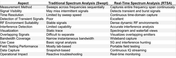 Table 1. Comparison of traditional swept spectrum analysis and real-time spectrum analysis for modern RF interference detection and 5G network testing.
How Are Real-Time Spectrum Analysis Workflows Changing Field Testing?
Table 1. Comparison of traditional swept spectrum analysis and real-time spectrum analysis for modern RF interference detection and 5G network testing.
How Are Real-Time Spectrum Analysis Workflows Changing Field Testing?
The traditional model of RF troubleshooting, dispatching teams to investigate issues on-site, is rapidly becoming unsustainable. Historically, diagnosing problems in the “last mile” required manual drive testing, consuming significant time, labour, and operational resources. That model is now shifting toward centralised, software-driven workflows.
By combining ruggedised handheld spectrum analysers with centralised analysis platforms, engineers can remotely control distributed test assets, monitor multiple sites simultaneously, and stream live measurement data back to centralised teams. This creates a fundamentally different workflow: capture, stream, analyse, and act. Engineers no longer need to be physically present at every field location. Instead, units can remain deployed at the edge while analysis happens centrally, powered by high-fidelity, wideband IQ data delivered in real time.
How Does Real-Time RF Interference Detection Use TDoA Localisation?The classic “fox hunt,” tracking interference sources with directional antennas, was built for a slower and simpler RF environment. In today’s dense 5G deployments, where interference sources can appear and disappear in milliseconds, manual methods struggle to keep pace. The modern approach shifts the problem from physical pursuit to mathematical computation. Time Difference of Arrival, or TDoA, techniques use multiple GPS-synchronised receivers to measure the precise arrival time of a signal across different locations.
Because RF propagation speed is constant, software can calculate the emitter’s position based on the difference in arrival times. This approach reduces reliance on slow, manual triangulation and enables rapid, wide-area localisation that scales with the complexity of modern networks. RF interference detection is no longer only a field exercise. It is increasingly a data-driven problem solved through coordinated measurement and computation.
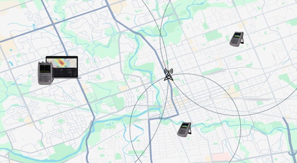 Figure 2. Distributed field measurements combined with TDoA processing enable rapid, wide-area localisation of interference sources
How Are Handheld Spectrum Analysers Closing the Gap Between Field and Lab Testing?
Figure 2. Distributed field measurements combined with TDoA processing enable rapid, wide-area localisation of interference sources
How Are Handheld Spectrum Analysers Closing the Gap Between Field and Lab Testing?
For years, RF engineers had to choose between portability and performance. Handheld spectrum analysers offered convenience in the field but often lacked the depth required for advanced analysis. Benchtop instruments delivered precision, but at the cost of mobility. That trade-off is now changing.
Modern handheld analysers can enable wideband real-time IQ streaming, representing a significant leap from previous limitations and changing what can be achieved outside the lab. This capability is especially important for 5G New Radio, where channel bandwidths can reach up to 100 MHz in sub-6 GHz bands. Without wideband capture, engineers may be forced to stitch together narrower measurements, losing critical time-domain behaviour in the process. With wideband streaming, entire 5G channels can be captured in a single acquisition, preserving signal behaviour and enabling integration into centralised analysis workflows. In practical terms, the boundary between field and lab is becoming less rigid. More advanced analysis can now be brought closer to where the RF problem actually occurs.
Why Real-Time Spectrum Analysis Is Becoming Essential for 5G Network TestingSpectrum management is undergoing a fundamental transformation. Detecting signals is no longer sufficient. Engineers must now be able to capture transient, wideband RF activity in real time, stream and classify that data within centralised systems, precisely locate interference sources, and act before disruptions escalate into failures.
The wideband reality is already here. With 5G NR channel bandwidths reaching up to 100 MHz in sub-6 GHz bands, real-time wideband capture is not just a forward-looking requirement. It is an immediate need for modern 5G network testing. The question is no longer whether interference will occur. The question is whether your tools can see it in time.
The post The 5G Radio Fog: Why Traditional Spectrum Analysers Miss Modern RF Interference appeared first on ELE Times.
PikeOS adds support for the rugged Kontron VX3060 board
SYSGO, a leading European supplier of real-time operating systems and hypervisors for safety and security-critical embedded applications, and Kontron, a global provider of IoT/Embedded Computing Technology (ECT), have announced the availability of a validated Board Support Package (BSP) for the rugged VPX Kontron VX3060 board, based on 11th generation Intel® Core processors. The new BSP extends the long-standing collaboration between the two companies, providing a reliable European hardware and software foundation for safety, security and mission-critical embedded applications.
Designed for demanding markets such as defence, transportation and industrial automation, the combined solution helps system developers speed up platform integration, taking advantage of PikeOS’s advanced virtualization and separation capabilities on a proven VPX computing platform.
 The Kontron VX3060 board with an 11th generation Intel Core processor, supported by the PikeOS BSP.
Developers can immediately deploy PikeOS on the Kontron VX3060 or on Kontron systems such as HARAKAN-F2 that integrate the VX3060, using a fully supported BSP, significantly reducing platform integration effort and accelerating the development of safe and mixed-criticality embedded systems. The BSP supports the board’s key features, including Ethernet, UART, thermal sensors, voltage monitoring sensors and mass storage interfaces. Additional platform security capabilities such as Trusted Platform Module (TPM) integration and Secure Boot are available on customer request to meet cyber resilience challenges and platform integrity requirements. The availability of the BSP accelerates time-to-market, shortens software bring-up times and gives developers a robust starting point for building certified and security-critical systems.
Mixed-criticality support and secure virtualizationThe Kontron VX3060 and the HARAKAN-F systems based on it are designed to operate in harsh operating environments and are suitable for transportation, defence, industrial automation and other applications that require rugged computing platforms. With PikeOS support, customers can immediately take advantage of PikeOS’s advanced partitioning and virtualization capabilities on the platform. PikeOS can operate as a secure hypervisor and as a combined hypervisor and real-time operating system, all in a single product. This flexibility allows developers to consolidate multiple applications with different criticality levels on a single hardware platform while maintaining strict separation between workloads. Critical real-time functions can run alongside Linux, middleware or application environments, enabling efficient mixed-criticality architectures that reduce system complexity, size, weight, power consumption and lifecycle costs.
Strengthening a European technology ecosystemAs demand for reliable European technologies continues to grow in critical sectors, the collaboration between SYSGO and Kontron offers customers an integrated technology stack, combining proven embedded hardware, real-time virtualization and advanced cybersecurity capabilities.
“Our customers increasingly expect embedded computing platforms to be backed by mature software ecosystems,” said Sébastien Vitre, Product Manager at Kontron. “By extending PikeOS support to the VX3060, we give developers a validated hardware and software platform that reduces integration effort and enables faster deployment of secure and mixed-criticality applications.”
“The availability of PikeOS on the Kontron VX3060 demonstrates the continued success of our cooperation with Kontron,” said Carsten Beck, Partner Management at SYSGO. “Together we provide customers with a European technology stack that combines rugged hardware, advanced virtualization, real-time capabilities and the security features needed for next-generation embedded systems.”
The BSP is available immediately and includes support for the main hardware interfaces needed for system boot and application development. Additional security features, including TPM-based trusted computing and Secure Boot, can be integrated according to customer requirements.
The post PikeOS adds support for the rugged Kontron VX3060 board appeared first on Open Electronics.
✅ Оголошується конкурс на заміщення посад
Національний технічний університет України "Київський політехнічний інститут імені Ігоря Сікорського" оголошує конкурс на заміщення вакантних посад. Термін подання документів до 25.10.2026 року.
Конкурс на заміщення вакантних посад завідувачів кафедр
Конкурс на заміщення вакантних посад професорів
Конкурс на заміщення вакантних посад доцентів, викладачів
NDA LAB KPI на Радіотехнічному факультеті

✔️ У КПІ ім. Ігоря Сікорського запрацювала NDA LAB KPI, лабораторія, яку створили спільно з рекрутинговою агенцією NDA Recruitment. Лабораторію відкрили на Радіотехнічному факультеті КПІ, щоб студенти працювали із сучасним обладнанням, перевіряли власні ідеї на практиці, проводили дослідження, створювали й тестували технічні рішення у сфері радіосистем, електроніки та інших технологій.
Paper MOD Player: The Amiga Never Dies
RobDevBuilds has built a MOD player that reads music data printed on paper. The project uses two cameras and stepper motors for optical reading. The goal is to preserve the Amiga’s legacy on a paper medium that could last longer than optical M-Disk discs. The MOD player is not a simple experiment: it is a complete system that plays MOD files by reading paper.
The paper disc and optical readingThe paper disc contains the MOD file’s patterns printed line by line, like in a tracker program. Each voice or instrument has columns of hexadecimal numbers. The back of the disc contains the audio samples and other necessary information, such as metadata and pattern sequence, encoded in a series of barcodes similar to QR codes.
The player uses two cameras, one for each side of the disc. Stepper motors move the cameras like a linear-tracking turntable. The front is read via OCR of the modified Amiga ‘Topaz’ font. The back contains the first 1084 bytes of the MOD file in an inspired QR format created by RobDevBuilds.
The project is documented on the Hackaday.io project page, where RobDevBuilds describes the building process and technical choices. Those who want to dig deeper can check the Hackaday.io project page to see the details of how it works.
Current limits and prospectsThe player currently cannot skip between patterns on the disc as quickly as some MOD files require. This is a known limitation of the project, which RobDevBuilds is addressing. Optical reading of paper is nonetheless a step forward for music file preservation.
The project proposes a method to preserve Amiga MOD files on paper, a medium that could last longer than optical M-Disk discs. Paper is durable and requires no electronics to be stored. Moreover, the printed format is readable even without the player, with OCR or by eye.
To recreate the project you need few components: two cameras, stepper motors, a control system, and a printed paper disc. The most delicate part is printing the patterns and QR codes, which must be precise for optical reading. The rest is mechanics and software, as in many maker projects.
- Two cameras to read the front and back of the disc
- Stepper motors for linear movement of the cameras
- OCR of the Amiga ‘Topaz’ font for the front
- Inspired QR format for the back with the first 1084 bytes of the MOD file
- Paper disc with patterns printed line by line
The paper MOD player is a project that combines music, retrocomputing, and printing. It is not a simple toy: it is a system that could ensure the survival of MOD files for decades, without needing specific hardware to read them. Paper is a medium that does not fear technological obsolescence.
Source: https://hackaday.io/contests
The post Paper MOD Player: The Amiga Never Dies appeared first on Open Electronics.
Pages




![[link]](https://i.redd.it/qn9vl0ye3crh1.jpeg)