


Feed aggregator
Unmasking the ghosts in your grid with power quality analyzers

Power that looks perfect can still betray you. Hidden distortions in the mains lurk behind flawless root mean square (RMS) readings—waiting to trip up even the best‑designed systems.
You’ve built the device exactly to spec, tested it in the lab, and watched it run flawlessly—only to have it mysteriously reset, flicker, or fail once deployed in the field. The nightmare begins when your trusty digital multimeter (DMM) or scope insists the mains are rock‑solid at nominal RMS, lulling you into false confidence.
In reality, hidden sags, swells, harmonics, and transients are wreaking havoc beneath that “perfect” reading. This is where a power quality analyzer (PQA) steps in—the engineer’s ultimate diagnostic lens for uncovering the real-world anomalies that standard tools simply cannot see.
An oscilloscope is the sprinter—built for speed, capturing fleeting microsecond transients in a narrow time window. It’s invaluable for spotting fast spikes but blind to the bigger picture.
A power quality analyzer (PQA), on the other hand, is the marathon runner—continuously logging over hours or days, aggregating long-term trends, tracking intense inrush currents during equipment startup, and checking compliance against standards like IEEE 519. Where the scope gives you snapshots, the PQA delivers the full story of your mains health.
Scopes give you snapshots, DMMs give you averages, but PQAs give you the truth—continuous visibility into harmonics, sags, swells, and transients that silently sabotage systems. If you want to design for the real world, you need to see the grid as it really is: noisy, imperfect, and unpredictable.

Figure 1 The PQ3198 power quality analyzer kit integrates specialized current clamps and voltage leads to capture and analyze transient grid anomalies. Source: Hioki
The rogue’s gallery of power quality villains
Three hidden villains—harmonics, sags and swells, and transients—quietly sabotage “perfect” power until a PQA exposes them.
- Harmonics – the waveform polluters: Nonlinear loads such as switching supplies, LED drivers, and variable frequency drives (VFDs) gulp current in pulses instead of smooth sine waves. Those pulses spawn integer multiples of the fundamental 50 Hz/60 Hz frequency. To quantify this mess, engineers look beyond total harmonic distortion (THD) to total demand distortion (TDD), preventing misleading percentage readings when equipment runs at light loads. In practice, “Triplen” harmonics—specifically the odd multiples of the third (3rd, 9th, 15th, etc.)—pile up in the neutral conductor, driving overheating, high crest factors, and insulation breakdown that can cripple systems.
- Sags and swells – the voltage rollercoaster: Large inductive loads like motors or HVAC compressors can drag voltage down to 85% of nominal, enough to brown‑out a microcontroller in an instant. On the flip side, when heavy loads shed or phases drift out of balance, the line can swell, stressing insulation and sensitive electronics. These rollercoaster swings slip past a DMM but are tracked relentlessly by a PQA.
- Transients – the semiconductor killers: Lightning strikes, capacitor bank switching, or routine grid events can unleash sub‑microsecond, high‑energy impulses. These spikes punch straight through ESD diodes and input protection, leaving semiconductors scarred or destroyed. A PQA captures these assassins in action, providing the context that scopes alone often miss.
Visual interpretation: The phasor diagram
One of the most practical screens on a PQA is the phasor display—a live map of voltage and current vectors that instantly reveals system health. A balanced three-phase system shows vectors neatly spaced at 120° with equal lengths, but any angular deviation or unequal magnitudes signal phase imbalance, a silent motor killer that drives counter-torque and winding stress.
Equally important is the power factor: the angular gap between voltage and current vectors tells the story of displacement power factor (DPF), with lagging angles exposing inductive loads and leading angles flagging capacitive behaviour. However, because modern switching supplies also introduce distortion power factor via harmonic wave shaping, a PQA is vital to calculate the true power factor—ensuring you aren’t paying penalties for hidden inefficiencies that standard meters completely miss.

Figure 2 A PQA plots three-phase voltage and current relationships on a central phasor diagram to analyze phase angles, magnitudes, and power quality metrics. Source: Neo Messtechnik
Two sidenotes
First, while engineers often use these terms interchangeably when looking at a PQA screen, there is a distinct technical difference: a vector diagram maps static, space-dependent quantities with a magnitude and a fixed directional orientation (like mechanical force or magnetic fields), whereas a phasor diagram is a frozen snapshot of a constantly rotating, time-dependent AC waveform.
Because all three phases in a stable grid spin at the exact same frequency, “stopping the clock” allows the PQA to display their angular relationships cleanly on a 2D plane. In short, all phasors can be mathematically treated and plotted as 2D vectors on a screen, but if it represents a repeating, alternating AC waveform, it’s technically a phasor.
Second, while traditional PQAs capture localized, steady-state anomalies, phasor measurement units (PMUs) provide real-time, wide-area situational awareness across modern power grids. By utilizing GPS time-synchronization, PMUs measure electrical waves across geographically disparate locations simultaneously.
They sample voltage and current waveforms at high speeds—typically 30 to 120 observations per second—to deliver time-stamped synchrophasor data. This precision tracking of phase angles and magnitudes allows grid operators to detect dynamic instabilities, monitor wide-area power oscillations, and prevent wide-scale blackouts in increasingly complex, renewable-heavy distribution networks.
Beyond the basics: Today’s PQA landscape
Modern PQAs go far beyond the fundamentals. They’re now Class A certified under IEC 61000‑4‑30 Edition 3, tuned to detect supraharmonics in the 2–150 kHz band from EV chargers, solar inverters, and LED drivers. They are capable of microsecond‑level transient capture with sampling rates approaching 1 MHz.
A sidenote on supraharmonics – the new phantom: Classic harmonics stop at the 50th or 63rd order, but these higher‑frequency disturbances don’t just stress wiring—they interfere with IoT devices, smart meters, and communication systems, making them a new frontier for power quality monitoring.
Take a real‑world example. During EV charger rollouts in several European cities, utilities discovered that chargers injecting switching noise around 20–25 kHz were confusing smart meters. The supraharmonic interference overlapped with PLC communication bands, causing meters to misreport consumption data and triggering billing errors. PQAs tuned for the 2–150 kHz band exposed the culprit, proving that supraharmonics aren’t just abstract lab phenomena—they can directly disrupt grid intelligence and customer trust.
At the same time, IEEE 519‑2022 has tightened harmonic distortion limits at the point of common coupling, reflecting today’s nonlinear load environment and ensuring compliance reporting is more rigorous than ever. With cloud dashboards, automated reporting, and integration into data centres, renewable systems, and utility grids, PQAs have become essential tools for navigating a world where distributed energy resources make power quality more unpredictable than ever.
Building a DIY power quality analyzer
Building a DIY PQA is an incredibly rewarding, multi-disciplinary challenge that bridges the gap between embedded design, real-time digital signal processing (DSP), and high-voltage safety. To accurately capture complex multi-channel dynamics—such as system unbalance, triplen harmonics, and ground faults—a scratch-built approach demands an agile microcontroller like the dual-core ESP32 sampling at upward of 10 kHz per channel to perform continuous Fast Fourier Transforms (FFTs) up to the 50th harmonic.
While developers looking to deploy high-speed, multi-channel discrete ADCs (such as the ADS131M08) can achieve synchronous sampling across all inputs without phase skew, those wanting to offload the heavy math entirely can leverage a specialized polyphase metering IC like the Analog Devices ADE7880.
ADE7880 utilizes an on-chip, hardware-isolated adaptive real-time monitoring (ARTM) harmonic engine to automatically track fundamental frequency drift and calculate full THD+N over SPI. No matter the architectural route, strict implementation of galvanic isolation via components like the ZMPT101B voltage transformer is non-negotiable to protect downstream hardware, and firmware must be thoroughly vetted using low-voltage AC-AC step-down transformers before introducing the system to live, lethal mains environments.

Figure 3. Simplified block diagram of ADS131M08 reveals a fully integrated, 8-channel signal chain architecture featuring independent PGAs, ΔΣADCs, digital filtering, and dedicated calibration blocks feeding into a centralized control interface. Source: Texas Instruments
Designing for the real world means accepting that the grid is noisy, unpredictable, and far from perfect. Hidden distortions, imbalances, and transients are not exceptions; they’re the rule. A PQA equips engineers to see beyond the illusion of “perfect power” and design systems that survive in the wild.
So, here’s the challenge: What’s the weirdest power‑quality phantom you’ve ever had to hunt down in the field? Share your story in the comments—because every anomaly teaches us something new about resilience.
 T. K. Hareendran is a self-taught electronics enthusiast with a strong passion for innovative circuit design and hands-on technology. He develops both experimental and practical electronic projects, documenting and sharing his work to support fellow tinkerers and learners. Beyond the workbench, he dedicates time to technical writing and hardware evaluations to contribute meaningfully to the maker community.
Related Content
- Power System Harmonic Analysis using ETAP
- Distortion in power amplifiers: the input stage
- Distortion in power amplifiers: the sources of distortion
- Signal integrity and power integrity analysis in 3D IC design
- Highly integrated approach to power system design in the AI era
The post Unmasking the ghosts in your grid with power quality analyzers appeared first on EDN.
Wireless Smart Dial with ESP32-C3 and BLE HID
A wireless smart dial replaces keyboard and mouse for repetitive operations: turn it to navigate menus, press it to send commands. Afraz Ali’s project uses an ESP32-C3 SuperMini board, an SH1106 128×64 OLED display, and a KY-040 rotary encoder. The whole thing works as a Bluetooth Low Energy HID controller, so the computer sees it as a wireless keyboard or mouse.
The main input is the KY-040 encoder: turning it scrolls through the menu on the display, pressing it selects the action. The ESP32-C3 then sends the corresponding command via BLE HID. The SH1106 OLED display is connected via I²C at address 0x3C and shows the interface. The encoder uses three GPIOs (CLK, DT, SW) with internal pull-ups configured by the firmware.
 Basic architecture of the project
The firmware includes separate profiles for Auto/Universal, Windows, macOS, Android, and iPhone/iPad. This choice handles BLE HID limitations across different operating systems. Custom text macros and settings are saved persistently using the ESP32 Preferences library. The source code is available in Afraz Ali’s repository, where you’ll find ready-to-upload Arduino sketches.
For programming you need Arduino IDE, the ESP32 Arduino package, the Adafruit GFX library, Adafruit SH110X, HijelHID_BLEKeyboard, NimBLE-Arduino, and Lynx Serial Monitor. The project includes 11 digital GPIOs (PWM) and 4 analog inputs (ADC) on the ESP32-C3 SuperMini board. Afraz Ali’s repository contains all the necessary code.
Power and consumption of the ESP32-C3 boardThe ESP32-C3 SuperMini board supports USB or external power from 3.3 V to 6 V. Sleep consumption is about 43 μA, so the device can stay in standby for a long time. Estimated build time is 5 hours, suitable even for those taking their first steps with ESP32 and BLE.
The M274 360-degree encoder module can be used as an alternative to the KY-040 for applications requiring continuous rotation. Both encoders connect directly to the board’s GPIOs. The 128×64 pixel SH1106 OLED display is the component that makes the interface readable and tidy.
 SH1106 OLED display
Assembly is simple: connect the OLED display via I²C at address 0x3C, wire the KY-040 encoder to the three GPIOs, and power the board via USB. The firmware handles the internal pull-ups, so no external resistors are needed. The project is compact and can be enclosed in a small 3D-printed case.
The dial works as a customizable physical control surface. You can assign keyboard shortcuts, multimedia controls, and text macros to each menu item. The device is useful for people working with editing, development, or office automation software.
- ESP32-C3 SuperMini Development Board
- SH1106 128×64 OLED
- KY-040 Rotary Encoder
- M274 360-Degree Rotary Encoder Sensor Brick Module
Afraz Ali’s project is a great starting point for understanding how BLE HID works and how to build a wireless input device. The wireless smart dial is a concrete example of how a small microcontroller can replace traditional peripherals.
Source: https://github.com/afrazali722/ESP32-C3-Smart-Dial-Custom-BLE-Menu-Controller
The post Wireless Smart Dial with ESP32-C3 and BLE HID appeared first on Open Electronics.
India’s Semiconductor Ecosystem Gets a Boost as Teradyne Opens Office in Bengaluru
The enthusiasm around the Indian semiconductor industry is palpable! While the government and domestic manufacturers have already started demonstrating their commitment through investments and project announcements, global technology suppliers are joining the optimism.
Confirming this positive trend, Teradyne, a leading provider of automated test equipment and advanced robotics, has announced the opening of an office in India focused on supporting semiconductor manufacturing, located in Bengaluru, Karnataka. The new office formalises Teradyne’s growing presence in the country and underscores the company’s long-term commitment to India’s semiconductor and electronics manufacturing industry. As AI drives demand across the full semiconductor supply chain – from wafer to data centre – this announcement will certainly provide a boost to the segment.
“India is at an inflection point in its semiconductor journey and establishing a permanent office in Bengaluru reflects our long-term commitment to this market,” said Greg Smith, President and CEO of Teradyne. “As India accelerates investment in domestic fabrication, packaging, and test capabilities, we intend to be a trusted partner to our customers, our government partners, and the broader ecosystem every step of the way. Establishing a local presence will help us move at the speed this industry demands.”
Teradyne Bets Big on IndiaThe Bengaluru office, located at Vesta Building, Bagmane Cosmos Tech Park, will serve as a local hub for customer engagement, applications support, training, and strategic partnerships, strengthening Teradyne’s ability to support India’s expanding base of chipmakers and electronics manufacturers as the country builds out high-volume manufacturing, packaging, and test capabilities.
The new office will support Teradyne’s broader India strategy, led by Alpa Sood, Country Manager, Teradyne, as the company deepens its presence across the country. The opening comes as India accelerates its semiconductor ambitions under the government’s India Semiconductor Mission, which is driving significant new investment in domestic fabrication and manufacturing infrastructure.
“Teradyne’s decision to establish a permanent office in India is a strong vote of confidence in India’s semiconductor growth story,” said Amitesh Kumar Sinha, chief executive officer of the India Semiconductor Mission, and additional secretary at the Ministry of Electronics and Information Technology. “As India scales its semiconductor fabrication, packaging, and test capabilities, the presence of a global leader such as Teradyne will further strengthen the semiconductor value chain and contribute to the development of a robust semiconductor manufacturing ecosystem in the country.
The post India’s Semiconductor Ecosystem Gets a Boost as Teradyne Opens Office in Bengaluru appeared first on ELE Times.
Offline Wikipedia on ESP32: a whole encyclopedia on a cheap display
Putting an entire encyclopedia on a cheap display moves knowledge from the center of the network to its edge. Alun Morris’s project does exactly that: it turns the ESP32-2432S028 module, the 320×240 pixel Cheap Yellow Display, into an offline Wikipedia reader. Articles, images, and the search index live on a microSD card, and the device reads them without any internet connection.
The result is a standalone device that responds to touch and shows encyclopedia entries. The base is the Kiwix ZIM file, the same format used by offline Wikipedia projects on desktop. A preprocessor on a PC converts it into a binary database optimized for the ESP32’s limited resources. The firmware reads all content from there.
The preprocessor and data conversionThe starting point is the recommended ZIM file, wikipedia_en_simple_all_maxi, a download of about 3.3 GB containing roughly 285,000 articles. The preprocessor, written in Python 3.9+, uses libzim to read the file and converts it into a binary database. The processed size of Simple English Wikipedia is about 10 GB on the card.
The conversion is not a simple copy: the preprocessor cleans the article HTML, reduces images, and converts them into formats the ESP32 can decode. Photos become JPEGs with a default quality of 90, diagrams use the QOI format. Thumbnails have a maximum size of 320×212 pixels. Articles are also split into 32 MB chunks and images into 4 MB chunks, so the firmware can read them without saturating memory.
The build takes about 30–60 minutes on a modern PC and uses up to 4 CPU cores. The result is a database with fixed-width 80-byte records for the title index. For search, the firmware loads a sparse index into RAM with one entry every 64 articles, occupying about 7 KB. This allows quickly finding the scan point without reading the entire index from the card.
Firmware and ESP32 memoryThe firmware is written for PlatformIO and runs on the ESP32-2432S028 module, which mounts the ILI9341 display and the XPT2046 touchscreen. Memory is the main constraint: the ESP32 has about 300 KB of usable heap, while typical ZIM clusters are 1–4 MB, too large to handle at once. That’s why the preprocessor splits everything into smaller chunks.
The firmware’s minimal renderer handles the cleaned HTML and shows decoded images with TJpgDec for JPEGs and the qoi library for diagrams. Title search uses the fixed-width binary index and the sparse index in RAM, so even with 285,000 articles the response is immediate.
On first boot, the firmware performs touchscreen calibration and saves the data to flash for subsequent boots. This way the user doesn’t have to repeat the procedure every time. The project is documented in Alun Morris’s repository, where you can find the complete code, the preprocessor, and build instructions.
MicroSD card and practical limitsThe microSD card must be at least 8 GB: processed Simple English Wikipedia takes about 10 GB, so a 16 GB card is the safe choice. The CYD handles cards up to 32 GB, while 64 GB cards might work but without guarantees. The ZIM file to download is a single 3.3 GB download.
The project uses easily available components. Besides the ESP32-2432S028 module, you only need a microSD card and a USB cable for firmware upload. No other modules or sensors are required. Everything is powered via USB, like the ESP32 board with USB Type-C connector that many makers already have in their lab, although for this project the specific board is the CYD.
The main limitation is language: the Simple English version is meant for those with a reduced vocabulary, not for in-depth consultation. Also, images are thumbnails, not original versions. However, for those who travel, work in areas without coverage, or want a standalone educational device, this offline reader is a concrete and low-cost solution.
Source: https://github.com/alunmorris/Offline-Wikipedia-ESP32/tree/master
The post Offline Wikipedia on ESP32: a whole encyclopedia on a cheap display appeared first on Open Electronics.
P.A.R.: a robot that draws pixel art by flipping disks
P.A.R. is a robot that draws black-and-white pixel art on a 37×18 grid of square disks called squisks. Instead of using a solenoid for each disk like traditional flip-disc displays, it uses a single mobile robot with a tool head to physically flip the disks. The result is a slower but much more economical process, suited to works of art.
The project is by Zimm, who built the robot with over a thousand 3D-printed parts and dozens of wires. The heart of the system is an Arduino Nano ESP32, which controls the two-axis CNC machine and manages the internet connection. The display is made up of 666 hand-assembled squisks, black on one side and cyan on the other.
The tool head and grid scanningP.A.R.’s tool head is custom-made and includes a color sensor, a servo motor, and a pin. Before printing, the robot performs a full scan of the grid with the color sensor to learn the current state of each squisk. This way it knows exactly which disks are already in the right position and which are not.
After the scan, the robot fetches the image from the request queue on the server. It flips only the squisks that need to change state, using the pin driven by the servo motor. Precision is key: each disk must be rotated 180 degrees to go from black to cyan or vice versa.
Once printing is complete, P.A.R. runs another scan to check for squisks that were not flipped correctly. If it finds errors, it corrects them right away. This verification loop makes the system reliable even with disks that might jam or not rotate perfectly.
Web connection and remote controlThe robot is connected to the internet via the Arduino Nano ESP32, which integrates Wi-Fi and Bluetooth. A dedicated website lets anyone send an image to print. The drawing is added to a request queue on the server, and the robot processes it when its turn comes.
This architecture makes P.A.R. an interactive installation: people can upload their own pixel art from any connected device. The code is available on GitHub, and Zimm’s project page collects the system details. The maker’s site also documents the hundreds of hours of work needed to build the robot.
For those who want to remake the project, the main components are few and accessible. The Arduino Nano ESP32 handles the logic and connectivity. The TCS3200 color sensor is a module with 4 white-light LEDs and a color-to-frequency converter, perfect for distinguishing the two sides of the squisks. The servo motor drives the pin that flips the disks.
The most challenging part is the mechanics. Over a thousand 3D-printed parts make up the frame, the axes, and the tool head. Assembling the 666 squisks requires patience and precision, but the result is a mechanical display unlike any other.
P.A.R. shows that you can build a low-resolution display without the cost of hundreds of solenoids. A single mobile robot, a smart tool head, and a bit of software are enough to turn a grid of disks into a pixel art canvas that can always be updated.
Source: https://par.zimmzimm.com/
The post P.A.R.: a robot that draws pixel art by flipping disks appeared first on Open Electronics.
Weekly discussion, complaint, and rant thread
Open to anything, including discussions, complaints, and rants.
Sub rules do not apply, so don't bother reporting incivility, off-topic, or spam.
Reddit-wide rules do apply.
To see the newest posts, sort the comments by "new" (instead of "best" or "top").
[link] [comments]
Radxa Linkr: A Pocket-Sized IP KVM for Browser-Based Remote Control
Radxa Linkr is a compact IP KVM that turns a computer into a machine you can control remotely, from anywhere. The device, about the size of a USB stick, connects to the target PC via HDMI for video and USB for keyboard and mouse. From then on, access happens through a web browser, with no need to install dedicated apps. You can manage the system even when it is off or during boot, for example to change BIOS settings.
Communication with the user happens over USB-C, Ethernet, or WiFi 6, in both client and access point modes. This means you can reach the device from a local network or from the internet, perhaps through a VPN. In addition, built-in support for Tailscale VPN and two-factor authentication makes the connection more secure. Everything is managed by a web interface that works on any operating system.
Hardware and components of Radxa LinkrThe heart of the device is the Rockchip RV1106G3 SoC, which integrates an Arm Cortex A7 CPU at 1.2GHz with a RISC-V co-processor. The 1 TOPS NPU handles AI processing, while the third-generation 5MP ISP and VPU support H.265/H.264 encoding up to 3072×1728 (5MP) at 30fps. System memory is 256MB DDR3L on-chip, with optional storage via a 16GB eMMC flash.
For video capture, the board uses an HDMI-to-MIPI CSI bridge (Rockchip RK682F) that supports inputs up to 2K at 30Hz. Connectivity is handled by a WiFi 6 module (AIC8800) and a RealTek RTL8152B Ethernet port. Power is 5V/2A via the USB-C port, and overall dimensions are just 70 x 22 x 12 mm. The price starts at $59 on AliExpress, Amazon, Arace, and Allnet.
The project page on the maker’s site documents the technical specifications and usage modes. In addition, the system supports advanced features such as integration with AI agents like OpenClaw and Hermes, which can automate diagnostic or maintenance operations on the remote computer.
Operation and browser accessAccess to Radxa Linkr happens through a web browser, with no dedicated software needed. Once the device is connected to the network, you open its web interface and configure the connection to the target computer. The interface shows real-time video and lets you use keyboard and mouse as if you were in front of the machine. You can also change the video resolution and manage multiple devices from a single panel.
The device also works before the operating system boots, so you can access the BIOS or bootloader. In addition, WiFi access point mode lets you connect directly to Linkr when no network is available. For those who need a stable connection, the Ethernet port offers a valid alternative to WiFi. Finally, the USB-C port can be used for power or for a direct connection to a PC.
 Radxa Link web interface
Power management is efficient thanks to the low-power SoC, but it is important to power Linkr with a 5V/2A adapter to ensure stability. As for cables, a good-quality HDMI cable is essential to avoid video interference. Also, if you want to extend the distance between Linkr and the computer, you can use a longer HDMI cable, but it is advisable to keep the USB connection short to avoid power issues.
A 5-meter HDMI 2.1 cable can be useful for placing the device in a convenient spot while maintaining video quality. However, for the USB port it is better to use a short, shielded cable. In addition, for those who want to expand logging capabilities, a MicroSD Card Reader module with SPI interface can be connected to save diagnostic data or video recordings.
Software and advanced featuresRadxa Linkr’s firmware is designed to be simple yet powerful. The web interface includes a management console that lets you configure the network, update the firmware, and manage users. In addition, Tailscale VPN integration simplifies secure remote connection, while two-factor authentication adds a layer of protection. For more advanced users, AI agents like OpenClaw and Hermes can be enabled to automate repetitive tasks.
The list of main features includes:
- Full remote access via browser, even before system boot
- WiFi 6 support in client and access point modes
- 10/100 Mbps Ethernet port via USB-C adapter
- Integrated Tailscale VPN and two-factor authentication
- Integration with AI agents like OpenClaw and Hermes
- H.265/H.264 video encoding up to 5MP at 30fps
In conclusion, Radxa Linkr is a versatile tool for anyone who needs to access their computers remotely, whether for work or personal use. Its compactness and advanced features make it an interesting choice for makers who want to experiment with remote control. With a starting price of $59, it is an accessible investment for those looking for a modern KVM over IP solution.
Source: https://linkr.now/
The post Radxa Linkr: A Pocket-Sized IP KVM for Browser-Based Remote Control appeared first on Open Electronics.
Testing a new CAN chip (TCAN3414DR), scope probes soldered directly to the pins
 | submitted by /u/m4rkw [link] [comments] |
Panasonic at Electronica: Next-gen Solutions for Industrial, Automotive, Telecom, and AI Applications on Display
Panasonic Industry seems to be driving innovation through consulting, designing, and supplying a wide range of technologies and systems to various industries. These include automotive, e-mobility, telecom, factory automation, infrastructure, manufacturing & logistics, and HVAC. the company participated in Electronica 2026 at Bengaluru and showcased its comprehensive portfolio of advanced technology Components and Solutions at the expo. The company has designed these solutions for diverse applications across Industrial, Automotive, Railways, Telecom, and Digital Infrastructure (Data Center) sectors during the Electronica India 2026, one of the world’s largest electronics expo held in Bengaluru.
A Wide Display of Cutting-edge TechnologyAt the exhibition, Panasonic introduced new technology of Fine Conductive Material, and EDLC (Electric Double Layer Capacitor), BLDC Motor, DC Pump and Polymer Capacitors for Data Center applications, along with the Electro-mechanical & Passive Components for Automotive (ADAS, EV ecosystem) and Industrial (smart meters, railways, automation) use cases, PCB Laminate Materials for high-frequency PCB solutions. These solutions have been designed to cater to India’s evolving Industrial and Automotive segments, significantly contributing towards enhancing performance, safety and reliability.
While inaugurating the Panasonic Industry stall at the Electronica India 2026, Hirokazu Kamoda, DMD, Panasonic Life Solutions India, said, “India’s electronics industry is entering a phase of accelerated transformation, with rapid growth across automotive, industrial, and digital infrastructure segments. At Panasonic, we are committed to enabling this transformation by bringing-in advanced, reliable, and sustainable component solutions rooted in Japanese innovation and tailored to meet Make-in-India vision. We are also implementing Digital initiatives to strengthen and expand our reach to the widespread customers across India, and create Digital Sales Platform to fulfil their requirements seamlessly with speed”.
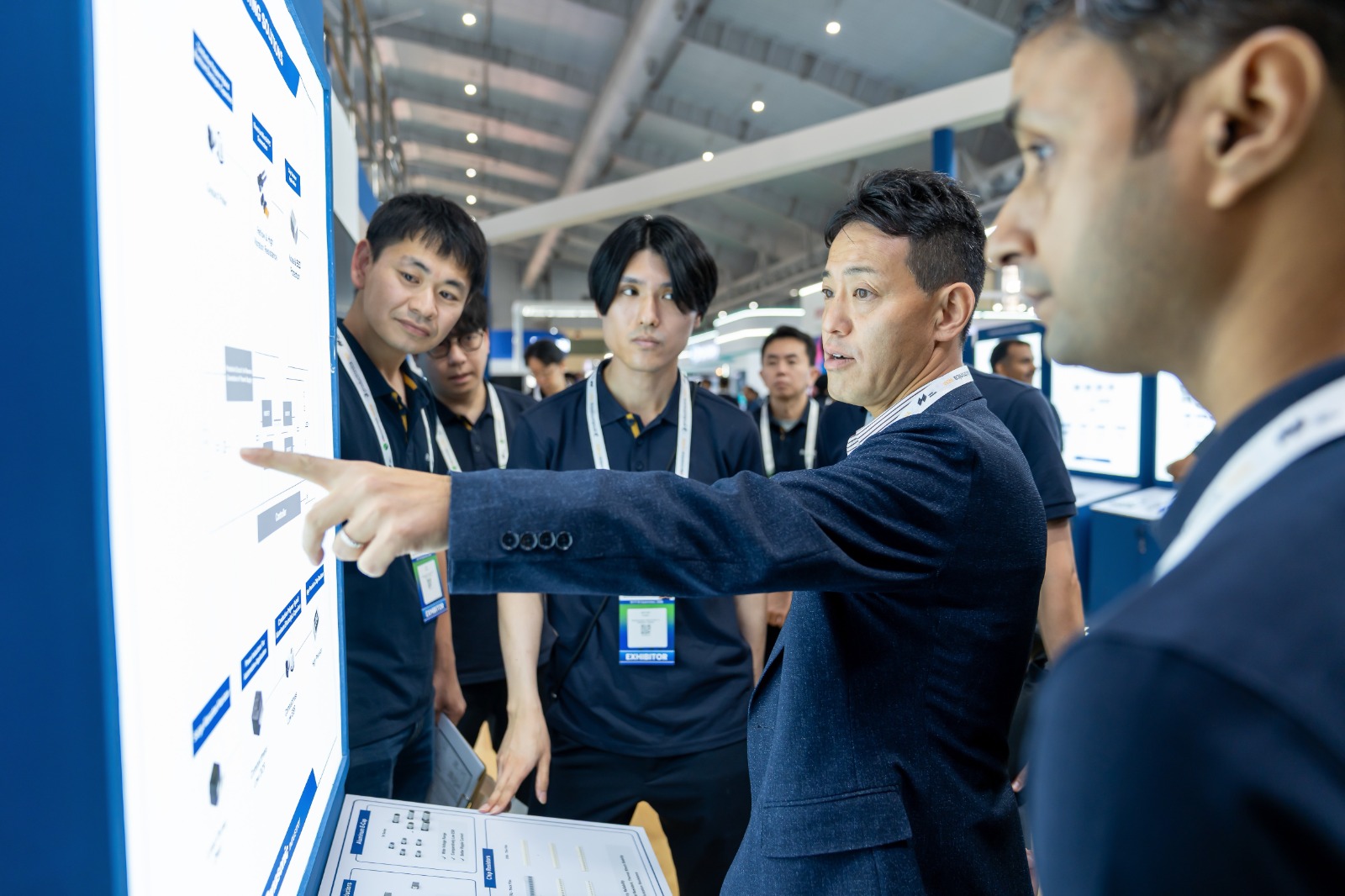
Naoki Nakazono, Managing Director, Global Sales Division, Panasonic Industry Co. Ltd., added, “Panasonic Industry has been supporting global innovation for over a century, and India is an increasingly important part of this journey. Through our participation at Electronica, we aim to showcase innovations and technologies that empower OEMs to drive efficiency, safety, and intelligence in applications ranging from AI and telecom to automotive and digital infrastructure.”
Further, Narayan Kumar, Chief Business Office, Panasonic Industry & Energy India (PIDEIN), Panasonic Life Solutions India (PLSIND), said, “We work very closely with our customers in India, who are looking for solutions that not only deliver performance but also ensure long-term reliability and cost efficiency. Whether it’s Polymer Capacitors for AI servers, high-frequency PCB laminate materials, or our new Fine Conductive Materials, every solution reflects our commitment to elevating their (customer/OEMs) manufacturing capabilities, which in turn advances industrial proficiency within the ecosystem in our country.”
The post Panasonic at Electronica: Next-gen Solutions for Industrial, Automotive, Telecom, and AI Applications on Display appeared first on ELE Times.
Tip: "no-clean" solder paste - clean it!
 | "no-clean" solder paste leaves really messy looking residues having fine pitch connectors (looks like a cracked salt deposition). The pictures show the before and after cleaning using an ultrasonic bath and flux remover agent (bath ph = 12, 50 °C, 5 min). Cleaning with isopropanol and flux-off using brushes did not work at all (hard to find a suitable brush, hair size vs hair hardness). Conclusion: Always clean your boards for best results. Connector pad specs: - 400 um pitch - 200 um pad width - 100 um mask dam (sliver) - 50 um mask expansion [link] [comments] |
Lumina Desk: The Restaurant Table That Takes Orders by Voice
Lumina Desk is a restaurant table that takes voice orders, without apps, QR menus, or waiters. A Raspberry Pi with microphone, speaker, and ePaper screen manages the entire cycle: the guest speaks, the system transcribes, interprets, shows the order on the display, communicates it to the kitchen, and collects payment via UPI QR. The project is by Shubhjaiswal408, and Shubhjaiswal408’s repository contains all the code to rebuild it.
The heart of the system is wake-word detection for ‘Hey Lumina’, handled by the on-device openWakeWord model. Once woken, the microphone captures the guest’s voice and transcribes it with Groq Whisper (whisper-large-v3-turbo) if there’s a connection, or with Vosk in offline mode. The text is then passed to an LLM, GPT-OSS-20B online or LFM2-700M offline, which interprets the intent. However, prices, wait times, and allergens are never left to the model: they are calculated in Python from the restaurant’s real menu.
For the most common requests, like ordering a pizza, asking for the bill, or checking an allergen, the system doesn’t even go through the LLM. A rule parser classifies them in under 5 ms, making the experience almost instantaneous. Additionally, the menu of the Auntyno-Z Pizza restaurant in Ghodasar includes 189 dishes, of which 66 are pizzas, and the parser handles them all without a hitch.
The data flow: from voice to order in the kitchenOnce the request is interpreted, the order state is published to an MQTT bus. Two services subscribe to this bus: the first generates an 800×480 pixel image and sends it to the ePaper panel on the table, so the guest sees the summary in real time. The second is the kitchen dashboard, which receives the order ready for preparation. This approach separates recognition logic from display, making the system modular and easy to extend.
Payment happens via a dynamic UPI QR code showing the exact bill amount. Payment confirmation is read directly from the merchant’s emails via IMAP, so the system knows when the order has been settled and can reset the table for the next customer. Everything runs on a single Raspberry Pi, which also handles confirmation audio through the speaker.
 The system runs entirely on a Raspberry Pi and keeps working without internet. (photo: Shubhjaiswal408)
The project aims to work even without an internet connection, an important choice for a noisy environment like a dining room. In offline mode, transcription uses Vosk and interpretation relies on the LFM2-700M model via Ollama. This 700M-parameter model runs on the Raspberry Pi’s CPU and takes about 9 seconds for processing. That’s an acceptable time for an order, but it shows the trade-off between accuracy and speed when working without the cloud.
To reduce wait times, the rule parser intercepts most phrases. For example, if the guest says ‘I’d like a margherita’, the parser recognizes the pizza, calculates the price from the menu, and publishes the order to MQTT without ever calling the LLM. This way, the system feels responsive in daily use and reserves the 9 seconds of computation only for more complex questions.
For voice synthesis of confirmations, the system uses Piper, a lightweight text-to-speech engine. Finally, image generation for the ePaper screen is handled by the Pillow library, which composes the order summary with high readability. Everything is orchestrated by Python scripts that communicate via MQTT, keeping the code clean and adaptable to other restaurants.
Anyone wanting to replicate the project will find in Shubhjaiswal408’s repository the code for speech recognition, menu management, and MQTT integration. The system was designed for a real restaurant with 189 dishes, so it’s not a demo: it’s a device that has faced noise, different languages, and the need for reliability. For hardware, the Raspberry Pi 5 with 2 GB is an adequate base, although the original project uses an earlier model. The 2 W speaker is sufficient for the short voice confirmations at the table.
Source: https://github.com/Shubhjaiswal408/lumina-desk-smart-restaurant
Related productsThe post Lumina Desk: The Restaurant Table That Takes Orders by Voice appeared first on Open Electronics.
Odisha Gears Up to Become a Force Worth Reckoning in India’s Semiconductor Growth Strategy
The state of Odisha has made its ambition clear: it intends to emerge as a leading semiconductor and electronics hub in the country. In a recent announcement from CM Mohan Charan Majhi at SEMICON India 2026, Odisha announced the development of an 870-acre Odisha Silicon Valley in Naraj, near Cuttack, which will host major Electronics & IT projects. This commitment comes alongside investment proposals worth approximately Rs 23,600 crore, with the potential to generate around 6,100 employment opportunities across the semiconductor and electronics ecosystem.
The CM led a series of high-level engagements with semiconductor and technology companies. The state is augmenting its growing investment pipeline to attract the next wave of investments across the semiconductor value chain. The engagements also saw the signing of a Letter of Intent (LoI) with QuadQuantum for a semiconductor facility to produce SiC Substrate wafers, further strengthening Odisha’s engagement with the semiconductor and technology ecosystem at SEMICON India 2026.
Why was Naraj Selected for Odisha’s Semiconductor Push?The area for Odisha Silicon Valley in Naraj offers a highly favourable strategic location regarding connectivity and industrial infrastructure. With seamless connectivity to the Cuttack–Bhubaneswar urban corridor, the site also provides efficient multimodal access to major ports such as Paradip and Dhamra, along with connectivity to key national highways. These advantages position Naraj as a potential strategic hub for the semiconductor supply chain, logistics and allied industries.
Semiconductor fabrication facilities and assembly units require reliable access to substantial quantities of water and power and the site’s proximity to the Mahanadi River provides a significant locational advantage for meeting industrial water requirements. Combined with its connectivity and infrastructure potential, Naraj offers a strong foundation for developing a world-class semiconductor and electronics ecosystem.
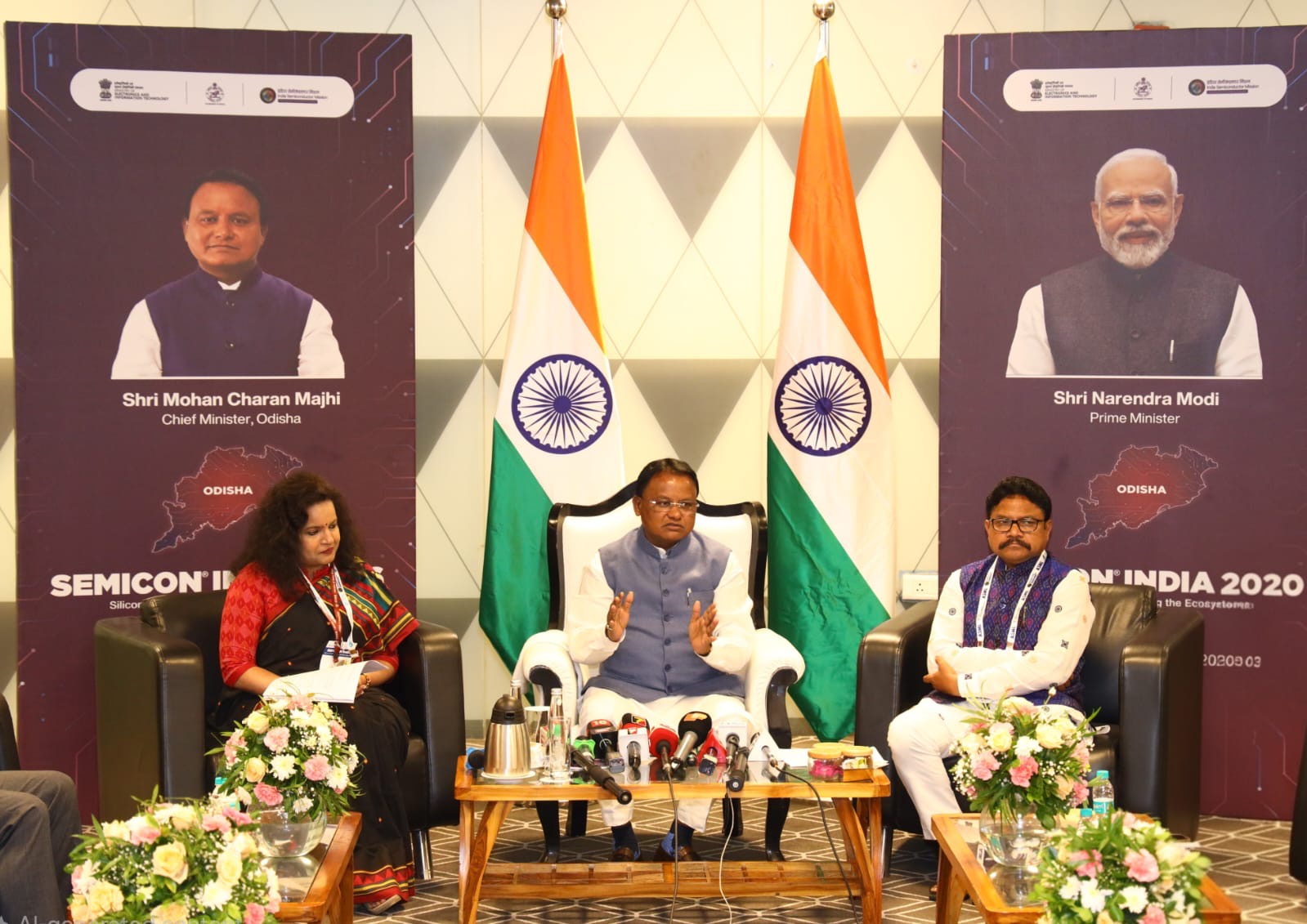
The engagements come as Odisha showcases the progress of its semiconductor journey at SEMICON India 2026. The Odisha Pavilion showcased projects from RIR Power, SiCSem, 3DGS, ARF Design and educational institutions designing the first batch of Made in India chips such as NIT Rourkela and PMEC Brahmapur.
From Sand to Silicon: Establishing the Semiconductor EcosystemOdisha’s journey towards building a semiconductor ecosystem is also being brought alive at the Odisha Pavilion through “Sand to Silicon”. The installation gives a distinctive Odisha expression to the state’s semiconductor journey, connecting its identity with its growing ambitions in silicon and advanced technology. It also ties into Odisha’s larger vision of moving from a “Mine Economy” to a “Mind Economy.”
Beyond the projects already underway, Odisha has been taking measures to build the wider ecosystem required to emerge as a leading semiconductor hub. The state has been among the early movers in aligning its Semiconductor Policy with the evolving India Semiconductor Mission 2.0. Its recent Third Policy Amendment further expanding support to critical parts of the semiconductor value chain.
Through the amendment, Odisha has extended 25% additional fiscal support to ISM-approved projects in semiconductor equipment manufacturing, semiconductor-grade gases, raw materials and supply-chain segments. The current policy framework also provides support for engineer relocation, manpower skilling, internships, international patents and R&D.
The post Odisha Gears Up to Become a Force Worth Reckoning in India’s Semiconductor Growth Strategy appeared first on ELE Times.
EEVblog 1774 - PayPal Here Part 2 - Security Boogaloo
Hello! I'm a beginner in electronics, and I've built a half-adder using 2N2222A.
 | submitted by /u/timofey2585 [link] [comments] |
CSconnected celebrates impact of Strength in Places Fund program
NewPhotonics and Tower begin high-volume shipments of laser-integrated, serviceable optical engine PICs for scale-out and scale-up AI interconnect
Tower highlighing high-volume silicon photonics and SiGe solutions at ECOC
onsemi unveils Embedded Power Platform
Mactini: the minimalist laptop built on an RP2350
The Mactini turns a satirical BBC meme into a real, working laptop. Tucker Osman built an ultra-small device with a single button that handles every function. The project shows how you can build a minimalist computer with modern components and salvaged materials. The technical documentation is complete, and the result is surprising in both size and engineering.
At the heart of the system is a small Waveshare board based on the RP2350. This board handles the display, audio, and input. The display is a 1.69-inch SPI LCD with an ST7789V2 controller. The resolution is enough for a basic text and graphics interface. Everything is housed in a 3D-printed case designed in FreeCAD.
Firmware and video handling with DMAThe firmware uses DMA to copy screen data, freeing up CPU cycles for other tasks. Video playback is handled through Motion JPEG decoding. This approach lets the device show animations and clips on the small display without overloading the processor. DMA also reduces latency and improves image smoothness.
Audio is handled by an iPad speaker and an amplifier salvaged from a scrap board. This recycling choice lowers costs and shows that parts from broken devices can be reused. The sound is clear, considering the size of the device. The mix of salvaged and modern components makes the project accessible.
3D-printed case and materialsThe case is 3D-printed and designed in FreeCAD. This open-source software lets you modify the design to suit your needs. The shell is compact and protects the internal components. 3D printing also lets you customize colors and finishes. The original project includes the files needed for printing.
To rebuild the project you need only a few key components: the Waveshare board with RP2350, the ST7789V2 display, and a salvaged speaker and amplifier. The full list is available in the documentation. In particular, anyone who wants to replicate the Mactini also needs a 3D printer and filament. The rest is soldering and patience.
The project is documented in detail. The project page on Hackaday.io collects photos, schematics, and a description of how it works. Tucker Osman also shared design choices and the difficulties he ran into. Anyone who wants to dig deeper can check that page to better understand each step. It is a valuable resource for anyone who wants to build their own Mactini.
The Mactini is an example of how a satirical idea can become a concrete object. The combination of a single button, a tiny display, and salvaged audio makes it unique. It also shows that you don’t need expensive parts to build a working computer. It is a perfect project for anyone who loves technical challenges and creative reuse.
Source: https://hackaday.io/contests
The post Mactini: the minimalist laptop built on an RP2350 appeared first on Open Electronics.
Some tips for electrical engineers

Chime in with your suggestions in the comments. We’ll even allow the mechanical engineers out there to participate. Well…maybe.
The following are a few of the tips, advice, rules, or guiding principles, I’ve discovered after many years of engineering and in various engineering positions. I’m not an expert in engineering management; this list is just items I’ve discovered from being in the engineering trenches (or should I say, cubes).
Do you have a memorable experience solving an engineering problem at work or in your spare time? Tell us your Tale
General engineering- Trust the math. We’re lucky to be in a profession where many design solutions can be derived using mathematics – it is more science than art. Use the math and trust its results.
- You can’t violate the laws of physics no matter how smart you are. I’ve been in a room when presentations have been made of a design, but where the basic concept violated some law of physics. These poor people spent a lot of time heading to the dead-end.
- Be clever only when it’s needed. Don’t design in an “interesting” part into a company project unless it is needed. Save that exploration for your home projects.
- Build on previous designs if you can. Reusing parts of a proven solution is very good for business, and for your career.
- Document everything – code, tests, schematics, simulations, sketches. This is for the next engineer and for possible patent filings. It leaves a nice trail of work done to get to a solution.
- Work on the biggest unknowns first. This brings the risk to a project down quickly. If these issues cannot be resolved, the project concept may be able to be changed to avoid the issue.
- Estimate a project’s tasks to 8-hour resolution – make a list of all pieces of the project – code to write, circuits to design, mechanical, docs, testing, etc. Typically, you bring a representative of each design section into a room for a number of days. You discuss all areas of the design down to the smallest detail. I have found that if you break it down to a one-day task level, your time estimates will be very accurate, and you also may discover some risks early. Also never assume an 8-hour workday means 8 hours of engineering – many things get in the way. I always use 80% for the actual engineering time in a day.
- Fight for your time estimates. Management may tell you that your time estimate is too long, and give you a number that is too short. If you do a deep estimate down to the 8-hour level, you should be confident of the estimate and you can, and should, defend it. Don’t get pushed into an impossible time line.
- Adding people to a project in the middle may slow it down. Management may say they will give you more people. It depends on the project and where in the project you are, but more people can also be a time-sapping burden.
- Focus on your piece and trust the others to focus on theirs. I often had people tell me how this other team will not be ready when their part is needed. This is for a project manager to worry about. Keep your eyes on your part and make sure you’re ready on time.
- There is a fog-of-war on large projects. Project details can get lost and confused, especially on a large project. Things get missed in the activity – this is one of the project managers main tracking jobs. Make sure your part is well documented and progress/issues well communicated.
- Always stay calm. Things will go wrong; project disasters will happen. If you stay calm during these times, you will see that fixing the issue will go much smoother.
- Make sure all applicable department managers have signed off on the product spec. If someone wants a change, all departments need to sign off after engineering re-quotes the time/cost requirement changes.
- Pay attention to anomalies. Anomalies are often dismissed, but these can be clues to an underlying problem. Document these anomalies for future reference.
- Ship what you tested – if you change anything, always retest. Don’t assume it will work.
- Use simulations but verify in the lab as there may be unaccounted-for parasitics. All components can have some level of parasitics; resistors can have capacitance and inductance. Capacitors can have resistance and inductance; capacitance values can change relative to the applied voltage. Inductors have resistance and winding to winding capacitance. Transistors, FETs, and all semiconductors can have various capacitance, inductive, and resistive parasitics. Don’t even get me started on crystals.
- None of us is irreplaceable. The company probably wouldn’t collapse if you were gone tomorrow. Management knows that – you need to know that, too.
- Take care of your career yourself. Don’t depend on your company to move you along in your career. Push for a position you want. Discuss wages if you want an increase. Work to get the training you want and need.
- Never assume a part can be substituted with one from a different manufacturer, product line, or value without retesting in the product.
- Understand basic practical thermodynamics as it applies to electronics design – this knowledge is needed often in electrical engineering (EE)-type projects. Calculations are needed when using things like heatsinks, PCB heat dissipation, thermal vias, active or convection cooling, heat pipes, etc. Much of this can be dealt with by an EE without the need for a mechanical engineer.
- Tell your manager that the first PCB assembly will have issues, the second works sometimes, and the third’s the charm. I’m not sure I’ve ever seen a PCB be perfect on the first pass (except maybe a very simple one). Problems can be EMI issues, schematic errors, assembly issues, pad/trace tweaks, mechanical issues, etc. The latest layout and simulation tools help a lot, but they won’t tell you that you spelled the company name wrong on the silkscreen.
- Don’t write obfuscated code. If it seems a bit cryptic, then document it well. ( I actually saw production code with the line “Bet you don’t know what this does”.)
- Stop using so many pointers.
- All code has bugs, even yours.
- Use a coding standard – consider MISRA guidelines.
- Use lots of comments – at the top of the program file, at the top of every procedure, the top of large conditionals, and on all cryptic statements.
- Adding your comments to AI-written code will help assure that you understand the code.
- No magic numbers in the code – if you have an actual number in a line of code, consider if it is better defined in something like a #define or const.
- Keep fixing code to remove all warnings from your compiled code – fix anything that shows an error code, at any level.
- Minimize the use of global level variables (I’m admittedly a serial violator of this crime.)
- Always check to see if pointers are in bounds. You may be creating unstable code along with security issues.
- Consider using AI, because it can often speed things up. Then again, though, it can also slow them down. My experience is that it can write very nice-looking code that typically compiles, but often there are subtle errors, especially on boundary conditions. So, don’t trust but verify, but suspect and test.
- Avoid dynamic memory allocation if you possibly can. This can very quickly lead to hard-to-understand crashes.
- Employees are expensive, and equipment is cheap if it speeds their work up. Get them what they ask for.
- Employee training is important – encourage and pay for expos and classes. Set up vendor presentations (and buy lunch).
- Encourage patent filings and implement bonuses for filed and granted patents. Patents are good for the company portfolio and the employee’s morale, as well as your recognition of support.
- All engineers have a type of engineering that they are good at. They may good at systems engineering, clean-sheet-of-paper designers (those that can design a device from scratch based solely on a concept) , lab test engineering, simulator/modeling, maintenance and component engineering, estimating/spec writing, customer facing or not, field engineering, analog and digital engineering, EMI/EMC experts, etc., etc. You wouldn’t assign a digital engineer to do a complex analog design; in the same fashion, don’t assign an engineer that’s good at analyzing field data to a clean-sheet-of-paper task (and vice-versa).
- If you lead, supervise, or manage, never ever micromanage. This is discouraging to an employee. If you think they’re not performing, ask if they need assistance. If you think they are in over their heads, back off their task list or move them to another task or project.
- The 50% rule – this is my rule that states that 50% of the information you get from a user, having an issue with a device you designed, will be misleading or untrue. That doesn’t (hopefully) mean that they lied. It means they exaggerated, interpreted what happened and gave you the interpretation, mis-remembered a sequence of events, or used incorrect terminology (for example, said that the device died instead of that the screen or keyboard locked up). All data from the field must be vetted before digging too deep. ( I’m being generous with 50% because I actually believe the occurrence of this is more like 75%.)
I’m sure all the engineers out there have many other tips to add to this list. Let’s see some of yours in the comments. We’ll even allow mechanical engineers to chime in.
Damian Bonicatto is a consulting engineer with decades of experience in embedded hardware, firmware, and system design. He holds over 30 patents.
Phoenix Bonicatto is a freelance writer.
The post Some tips for electrical engineers appeared first on EDN.
Pages




![[link]](https://i.redd.it/gh5anpypzgqh1.png)