


Feed aggregator
Critical Manufacturing to Showcase MES-Powered Industrial Operations Platform for Intelligent Semiconductor Manufacturing at SEMICON India 2026
Critical Manufacturing, the Industrial Operations Platform company that unites execution, connectivity, analytics and trusted AI, will exhibit at SEMICON India from September 17–19, demonstrating how semiconductor manufacturers can establish connected, data-driven operations that support intelligent production.
Exhibiting in collaboration with ASMPT, Critical Manufacturing will bring its vision of the factory of the future to life, showing how manufacturers can transform operational complexity into actionable intelligence through a unified platform.
India is moving from semiconductor ambition towards ecosystem development, with investment spanning fabrication, compound semiconductors, assembly and testing, advanced packaging and chip design. As new manufacturing capacity is established, companies will need to build digital production foundations that can support quality, traceability and coordination from the outset.
From execution to intelligenceAt SEMICON India, Critical Manufacturing will demonstrate how its Industrial Operations Platform extends beyond traditional Manufacturing Execution Systems (MES). MES acts as the execution core within a broader platform that continuously connects production data, analytics and AI, enabling a closed-loop system where insights are generated and acted upon in real time.
For manufacturers developing new semiconductor operations, decisions made at an early stage can shape production performance for years to come. Establishing consistent processes, data structures and traceability from the beginning helps prevent fragmented systems from developing as facilities, product portfolios and production volumes grow.
The platform captures data at source, structures it across equipment, systems and sites, and provides the operational context needed to support informed decisions. This gives manufacturers a foundation that can scale with their operations while maintaining control over quality and production processes.
Experience the Factory of the FutureVisitors will be invited to “step into the factory of the future” through live demonstrations showing how machines, processes and data can be connected across the shopfloor.
The demonstration will highlight how real-time information flows between equipment and manufacturing systems, helping teams understand relationships between process conditions and production outcomes. This supports a shift from reacting to problems towards anticipating and addressing issues before they affect quality, output or delivery.
Together, these capabilities reflect the industry’s transition from digital transformation to intelligence-driven operations. By incorporating connectivity and manufacturing intelligence from the beginning, manufacturers can support continuous learning and improvement while avoiding isolated systems that later become difficult and costly to integrate.
“India has an important opportunity to build modern semiconductor operations without being constrained by the fragmented legacy systems found in many established manufacturing environments,” said Weng Keong Lan, Managing Director of Critical Manufacturing Malaysia, responsible for India’s Go-to-Market. “As new facilities and capabilities are developed, manufacturers can put the right execution, connectivity and data foundations in place from the outset rather than attempting to integrate them later.”
AI copilots for smarter decision-makingA key feature of the demonstration will be Critical Manufacturing’s AI Copilots, embedded directly within the MES environment. The copilots enable users to interact with manufacturing data using natural language and generate dashboards, charts and insights without complex queries or specialist expertise.
By making production information easier to access and interpret, AI Copilots can help engineers, operators and decision makers investigate changing conditions, identify trends and respond with greater confidence.
A joint approach with ASMPTThe joint presence with ASMPT reinforces the importance of considering manufacturing equipment and software as part of one coordinated production environment. Closely connected equipment and software ecosystems can provide greater coordination, control and performance across the production lifecycle.
Lan added, “At SEMICON India, we will demonstrate how a unified Industrial Operations Platform can help manufacturers standardise processes, establish end-to-end traceability and maintain control as production scales. Building these capabilities early will be essential if India’s growing semiconductor ecosystem is to translate investment into reliable, high-quality manufacturing.”
Experience the platform in actionVisitors to SEMICON India 2026 can experience live demonstrations at the ASMPT booth 1346, where Critical Manufacturing experts will showcase how the Industrial Operations Platform supports connected and intelligent semiconductor manufacturing.
Attendees are invited to explore how the platform can help manufacturers establish scalable operations, maintain production traceability and manage increasing complexity as facilities and output grow.
The post Critical Manufacturing to Showcase MES-Powered Industrial Operations Platform for Intelligent Semiconductor Manufacturing at SEMICON India 2026 appeared first on ELE Times.
Microchip’s 1.2V Clock Buffers Link Latest SoCs and FPGAs with Higher Voltage Components
The demand for low-voltage clock drivers continues to grow with the rapid adoption of advanced FinFET process nodes used in high-performance FPGAs, SoCs, AI accelerators and next-generation CPUs. Printed circuit board designers face increasing challenges due to the limited availability of standard 1.2V LVCMOS clock buffers and level-translating buffers capable of converting higher-voltage clock signals to the lower-voltage levels required by these advanced devices. Conventional approaches that rely on discrete components and voltage-divider techniques can compromise signal integrity and clock duty cycle accuracy while increasing board complexity and component count.
Microchip Technology has introduced the SY757xx family, a comprehensive portfolio of 1.2V-output LVCMOS clock buffers, designed to address these challenges. The new devices simplify system design by eliminating the need for traditional discrete component implementations while delivering ultra-low additive jitter performance. To provide flexibility for supporting legacy board power supplies and different clock-source voltage levels, the devices support a broad range of supply voltage (VDD) and a wide operating frequency range. The SY757xx family enables ultra-low additive jitter clock distribution while maintaining the high clock resolution and signal integrity required for today’s high-speed FPGA, SoC and CPU platforms.
“Our SY757xx family of clock buffers helps customers overcome the growing clock distribution challenges associated with next generation high-performance FPGA, SoC and CPU platforms,” said Maamoun Abou Seido, appointed vice president of Microchip’s timing and communications business unit. “By combining ultra-low additive jitter performance with broad VDD and wide frequency support in a single-chip solution, the SY757xx devices simplify board design, reduce component count and help customers maintain the signal integrity and timing accuracy required in today’s high-performance computing applications.”
Microchip’s SY757xx family strengthens the clock buffer’s role as a critically important SoC and FPGA interface for clock distribution and clock fanout functionality in application platforms where signal integrity is paramount. These platforms demand high-speed parallel processing, hardware reconfigurability, low latency and efficient real-time computing. These capabilities are required for applications ranging from embedded vision and video processing to AI/ML acceleration, industrial control and IoT, networking and communications, and signal processing and embedded systems.
Launching three products in production and eight that are sampling in limited volumes, the family spans a wide array of configurations in three space-saving packaging options. The devices protect against clock distortion across a 0 Hz to 250 MHz frequency spectrum while also offering a broad range of power supply input and output options across the 1.2V to 3.3V voltage-translation input range. This includes a single-chip option that reliably interconnects 3.3V components to FPGAs and SoCs with a 1.2V clock signal requirement. Additive jitter is as low as 26 femtoseconds (fs).
Compared to traditional discrete component solutions for these FPGA and SoC applications, the Microchip buffers simplify design and reduce bill-of-materials costs while helping to optimize AC coupling and biasing and maintain signal integrity. Voltage dividers using discrete components may not provide adequate design margin and can degrade signal integrity by causing duty-cycle distortion.
Microchip clock buffers complement the company’s comprehensive range of flash-based FPGAs and SoC FPGAs spanning ultra low density to mid-range density devices. These and other Microchip products that range from microcontrollers and analog components to power management, timing, connectivity and memory devices are pre-engineered and validated to enable a simplified, lower-risk and more holistic approach to system design.
The post Microchip’s 1.2V Clock Buffers Link Latest SoCs and FPGAs with Higher Voltage Components appeared first on ELE Times.
Y2K Wrist Sequencer: Retro Music with ESP32
The Y2K wrist sequencer is a musical device worn like a watch. It composes music by selecting sounds for each step and playing them back in sequence. The transparent 3D-printed case and snap-band bracelet make it a fashion accessory as well as an instrument. The project comes from 3DSage, who chose simple components and a retro aesthetic that hits the mark.
The heart of the system is an ESP32, which handles the sequencer logic and sound generation. A rotary encoder enables the standard sequencer workflows: scroll through steps, select a sound, and store it in the desired position. The LCD display shows the state of the composition, while the speaker plays the tones. There is also a headphone jack for private listening.
How the Y2K wrist sequencer worksThe operation is simple and straightforward. For each step, the user selects a sound to store in that position, such as a square-wave A note at 440Hz. The rotary encoder allows navigating between options and confirming choices. The touch pins, made from brass bar, cover an octave and make the device work more like a Stylophone synthesizer. The sequential playback lets you hear all stored sounds, creating a rhythmic melody.
The ESP32 can produce more complex waveforms, but the basic square-wave tones chosen for the default sounds fit the aesthetic perfectly. This approach keeps the project simple and true to the Y2K spirit. Additionally, the choice of a rechargeable AA battery makes the device portable and easy to recharge. The transparent PETG case adds a visual touch that recalls late-1990s gadgets.
Why this project is interestingIt is a simple and stylish way to make music, with a retro Y2K aesthetic that hits the nostalgia sweet spot. You don’t need to be a synthesis expert to use it: the controls are immediate and the visual feedback on the display guides you step by step. Moreover, the project is fully reproducible with easily available components. To get started you need only a few parts: an ESP32 board with 32 GPIOs, a 12mm rotary encoder with knob, and a 0.25-watt speaker. The transparent case is printed in PETG, the same material chosen by 3DSage.
The choice of the rotary encoder is spot-on for physical interaction: rotation and pressure give tactile feedback that recalls old synthesizers. The brass pins, on the other hand, add a live performance element. The result is a device that can be used both for planned composition and for improvisation. Thanks to the transparent case, you can see the internal circuit, a detail makers will appreciate.
How to remake the projectTo build the Y2K wrist sequencer you need few components. Besides the ESP32, you need a rotary encoder, an LCD display, a speaker, and a rechargeable AA battery. The touch pins are made from a brass bar, while the case is 3D-printed in transparent PETG. The snap-band bracelet completes the wearable design.
- ESP32 for logic and sound generation
- Rotary encoder for navigation and selection
- LCD display for visual feedback
- Speaker and headphone jack for audio output
- Rechargeable AA battery for power
- Brass bar for touch pins
- Transparent PETG for the 3D-printed case
Assembly requires some soldering and 3D printing of the case. Once assembled, the device is worn on the wrist and you can start composing. The sequential playback makes everything immediate: press the pins, select sounds, and listen to the result. The 3DSage video shows the step-by-step build, from printing the case to mounting the brass pins.
For power, a rechargeable AA battery is sufficient thanks to the ESP32’s low consumption. If you want to experiment with other boards in the ESP32 family, you can easily adapt the code. The project is a great starting point for anyone wanting to explore music synthesis with open-source hardware. Finally, the transparent case is customizable: you can change the color or add decorations.
Source: https://youtu.be/RrWw1gm3UEo?si=SbXtYVeqWxJHxh0B
Related productsThe post Y2K Wrist Sequencer: Retro Music with ESP32 appeared first on Open Electronics.
Y2K Wrist Sequencer: Retro Music with ESP32
The Y2K wrist sequencer is a musical device worn like a watch. It composes music by selecting sounds for each step and playing them back in sequence. The transparent 3D-printed case and snap-band bracelet make it a fashion accessory as well as an instrument. The project comes from 3DSage, who chose simple components and a retro aesthetic that hits the mark.
The heart of the system is an ESP32, which handles the sequencer logic and sound generation. A rotary encoder enables the standard sequencer workflows: scroll through steps, select a sound, and store it in the desired position. The LCD display shows the state of the composition, while the speaker plays the tones. There is also a headphone jack for private listening.
How the Y2K wrist sequencer worksThe operation is simple and straightforward. For each step, the user selects a sound to store in that position, such as a square-wave A note at 440Hz. The rotary encoder allows navigating between options and confirming choices. The touch pins, made from brass bar, cover an octave and make the device work more like a Stylophone synthesizer. The sequential playback lets you hear all stored sounds, creating a rhythmic melody.
The ESP32 can produce more complex waveforms, but the basic square-wave tones chosen for the default sounds fit the aesthetic perfectly. This approach keeps the project simple and true to the Y2K spirit. Additionally, the choice of a rechargeable AA battery makes the device portable and easy to recharge. The transparent PETG case adds a visual touch that recalls late-1990s gadgets.
Why this project is interestingIt is a simple and stylish way to make music, with a retro Y2K aesthetic that hits the nostalgia sweet spot. You don’t need to be a synthesis expert to use it: the controls are immediate and the visual feedback on the display guides you step by step. Moreover, the project is fully reproducible with easily available components. To get started you need only a few parts: an ESP32 board with 32 GPIOs, a 12mm rotary encoder with knob, and a 0.25-watt speaker. The transparent case is printed in PETG, the same material chosen by 3DSage.
The choice of the rotary encoder is spot-on for physical interaction: rotation and pressure give tactile feedback that recalls old synthesizers. The brass pins, on the other hand, add a live performance element. The result is a device that can be used both for planned composition and for improvisation. Thanks to the transparent case, you can see the internal circuit, a detail makers will appreciate.
How to remake the projectTo build the Y2K wrist sequencer you need few components. Besides the ESP32, you need a rotary encoder, an LCD display, a speaker, and a rechargeable AA battery. The touch pins are made from a brass bar, while the case is 3D-printed in transparent PETG. The snap-band bracelet completes the wearable design.
- ESP32 for logic and sound generation
- Rotary encoder for navigation and selection
- LCD display for visual feedback
- Speaker and headphone jack for audio output
- Rechargeable AA battery for power
- Brass bar for touch pins
- Transparent PETG for the 3D-printed case
Assembly requires some soldering and 3D printing of the case. Once assembled, the device is worn on the wrist and you can start composing. The sequential playback makes everything immediate: press the pins, select sounds, and listen to the result. The 3DSage video shows the step-by-step build, from printing the case to mounting the brass pins.
For power, a rechargeable AA battery is sufficient thanks to the ESP32’s low consumption. If you want to experiment with other boards in the ESP32 family, you can easily adapt the code. The project is a great starting point for anyone wanting to explore music synthesis with open-source hardware. Finally, the transparent case is customizable: you can change the color or add decorations.
Source: https://youtu.be/RrWw1gm3UEo?si=SbXtYVeqWxJHxh0B
Related productsThe post Y2K Wrist Sequencer: Retro Music with ESP32 appeared first on Open Electronics.
PRAMA’s Tourism Security Solutions Helps Secure Tourists and Tourist Sites
India is one of the favourite destinations for international tourists, but security concerns often curtail the opportunities and growth prospects. The Indian tourism sector needs to tap this opportunity by sprucing up its act with adequate security measures and adoption of the latest security technologies to assure the large pool of tourists travelling to India’s popular tourist destinations.
When planning a security strategy for the tourism sector, one needs to understand the key challenges and threats that exist in India’s vast tourism sector. The Indian tourism sector includes popular tourist destinations, national monuments and cultural heritage sites. Religious tourism offers diverse options for tourists; there are many world-famous places of worship in India that attract millions of visitors from around the world. India offers a wealth of opportunities for religious tourism, attracting millions of pilgrims and spiritual seekers from around the world.
Tourism Security ChallengesTourism in India faces several security challenges that can impact both domestic and international travelers. Here are some of the key issues:
Safety and Security: Concerns about the safety of tourists, especially women, have been prominent. Incidents of theft, harassment, and even violence have been reported, which can deter potential visitors.
Infrastructure: Inadequate infrastructure, including poor transportation and healthcare facilities, can pose risks to tourists. This includes issues like unsafe roads and lack of emergency medical services.
Environmental Degradation: Overcrowding and lack of proper waste management at popular tourist spots can lead to environmental degradation, which not only affects the natural beauty but also poses health risks.
Regulatory Challenges: The tourism sector often faces regulatory hurdles, including complex visa processes and inconsistent enforcement of safety regulations.
Human Resources: There is a shortage of skilled manpower in the tourism and hospitality sectors, which can affect the quality of services and safety measures available to tourists.
Security & Safety Awareness: Insufficient media promotion about tourism security and safety awareness protocols and guidelines lead to uncertainity and misinformation among tourists.
Addressing these challenges requires coordinated efforts from the government, private sector, and local communities to ensure a safe and enjoyable experience for all tourists.
How Security Solutions Can Help the Tourism SectorAdvanced video security solutions can significantly enhance the safety and security of tourists in several ways:
Video Security and Monitoring: High-definition cameras installed at key tourist spots, hotels, and public transport hubs can monitor activity in real time. This helps quickly identify and respond to any suspicious behaviour or incidents.
Crime Deterrence: The presence of visible security cameras can deter potential criminals. Knowing they are being watched reduces the likelihood of theft, vandalism, and other crimes.
Incident Response: In the event of an incident, video footage can provide crucial evidence to law enforcement agencies. This helps in the swift resolution of cases and enhances the overall sense of security.
Crowd Management: Video analytics can help manage large crowds at popular tourist destinations. By analysing foot traffic patterns, authorities can prevent overcrowding and ensure smooth movement of people, reducing the risk of accidents.
Emergency Situations: In emergencies, such as natural disasters or terrorist attacks, video security can provide real-time information to emergency responders, helping them to coordinate their efforts more effectively.
Enhanced Visitor Experience: By ensuring a safe environment, video security solutions can enhance the overall visitor experience. Tourists are more likely to enjoy their stay and recommend the destination to others if they feel secure. Implementing these solutions requires collaboration among local authorities, private-sector stakeholders, and technology providers to create a comprehensive security network that prioritises the safety and well-being of tourists. Places of worship face several unique security challenges, balancing the need to be open and welcoming with the necessity of ensuring safety. Here are some of the key challenges:
Open Access: Places of worship are designed to be open and accessible to everyone, which can make it difficult to control who enters and exits the premises.
Vandalism and Theft: These locations can be targets for vandalism and theft, especially if they house valuable artefacts or donations.
Violence and Terrorism: Unfortunately, places of worship can be targets for violent attacks, including hate crimes and terrorism. Ensuring the safety of congregants during services and events is a significant concern.
Cybersecurity: With the increasing use of digital systems for managing operations and communications, places of worship are also vulnerable to cyberattacks. This includes threats like ransomware, data breaches, and online harassment.
Emergency Preparedness: Many places of worship may lack comprehensive emergency response plans. This includes preparedness for natural disasters, medical emergencies, and other unexpected incidents.
Addressing these challenges requires a holistic approach that includes physical security measures, community engagement, and emergency preparedness planning. Collaboration with local law enforcement and security experts can also enhance the safety and security of these important community spaces.
Securing Places of Worship: Installing video security cameras and security systems can significantly enhance safety and provide peace of mind for devotees. By implementing these measures, places of worship can create a secure environment that allows congregants to focus on their spiritual activities without safety concerns.
Protecting Cultural Heritage Sites: It requires a combination of advanced security systems and thoughtful planning to preserve their historical and aesthetic value. By combining advanced security measures, cultural heritage sites can be effectively protected while maintaining their historical integrity and ensuring a safe and enjoyable experience for visitors.
PRAMA Solutions Secure Tourist Locations & TouristsPRAMA offers advanced Security Solutions for Tourism, Cultural Heritage Sites and Religious Places. PRAMA offers a range of specialised security solutions tailored for tourism, cultural heritage sites, and religious places.
Here are some of the key offerings for the tourism sector:
Smart Video Security Systems: These include advanced CCTV cameras with AI capabilities for real-time monitoring and threat detection. The systems are designed to ensure the safety of tourists and protect valuable cultural assets.
Integrated Remote Monitoring Intrusion Solutions (IRMIS): This solution enables centralised monitoring across multiple sites, providing a comprehensive security overview and rapid response capabilities.
AI Sense Solutions: Utilising artificial intelligence, these solutions enhance security by identifying potential threats and unusual activity, enabling proactive measures.
Advanced Traffic Management Systems (ATMS): These systems help manage and monitor traffic around tourist sites and religious places, ensuring smooth and secure access for visitors.
Specialised Temple Solutions: Tailored for religious places, these solutions include high-definition cameras and access control systems to manage large crowds and ensure devotees’ safety. PRAMA India’s solutions are designed to provide robust security while maintaining the sanctity and accessibility of cultural and religious sites.
The post PRAMA’s Tourism Security Solutions Helps Secure Tourists and Tourist Sites appeared first on ELE Times.
Murata Expands Automotive-Grade Metal Power Inductor Line-up with Nine New Inductance Values
Murata Manufacturing Co., Ltd. has expanded the line-up of its automotive-grade metal power inductors in the DFE2MCPH_JL series by adding nine new inductance values. This expanded line-up enables broader support for the diverse circuit design requirements of automotive power circuits used in advanced driver assistance systems (ADAS), in-vehicle infotainment (IVI), and other automotive electronic equipment. Mass production has already begun.
In recent years, the increasing performance and functionality of ADAS and IVI systems have driven demand for automotive power circuits that are smaller, more efficient, and lower in power loss. At the same time, increasingly diverse power supply requirements across different applications have created the need for a wider range of inductance values, allowing designers to select the most suitable inductor for each power circuit.
To address these market requirements, Murata has added nine new inductance options to the DFE2MCPH_JL series. Despite their compact 0806-inch (2.0 × 1.6 mm) package, the new inductors achieve low DC resistance, high current capability, and 40 V withstand voltage. They are also compliant with the AEC-Q200 automotive qualification standard, making them well suited for power circuits used in increasingly sophisticated automotive electronics, including ADAS and IVI systems. By expanding the available inductance range, Murata enables designers to select the optimum inductance value according to application and power supply requirements, thereby improving design flexibility for automotive power circuits.
Murata will continue expanding its line-up of automotive-grade power inductors to meet evolving market needs and contribute to further advances in vehicle performance, functionality, and electrification.
≪DFE2MCPH_JL Seres Specifications≫
| Category | Part Number | Inducta-nce
Nomina l value (μH) |
Tolerance | DC
Resistance (Ω) Max |
Typ. |
Related current (mA) Based on
Inductance Change Max. |
Typ. |
Based on
temperature Rise Max. |
Typ. |
| New | DFE2MCPHR10MJLL
Q |
0.10 | ±20% | 0.01
0 |
0.00
7 |
11100 | 13900 | 7500 | 9400 |
| New | DFE2MCPHR15MJLL
Q |
0.15 | ±20% | 0.01
2 |
0.00
9 |
8400 | 10500 | 6500 | 8200 |
| New | DFE2MCPHR22MJLL
Q |
0.22 | ±20% | 0.01
5 |
0.01
2 |
8200 | 10200 | 5600 | 7000 |
| Existing | DFE2MCPHR33MJLL
Q |
0.33 | ±20% | 0.01
8 |
0.01
4 |
6900 | 8100 | 5100 | 6400 |
| Existing | DFE2MCPHR47MJLL
Q |
0.47 | ±20% | 0.02
2 |
0.01
9 |
5400 | 6300 | 4400 | 5500 |
| New | DFE2MCPHR68MJLL
Q |
0.68 | ±20% | 0.04
0 |
0.03
1 |
4400 | 5500 | 3400 | 4200 |
| New | DFE2MCPH1R0MJLL
Q |
1.0 | ±20% | 0.04
8 |
0.04
1 |
3900 | 4900 | 2900 | 3700 |
| New | DFE2MCPH1R5MJLL
Q |
1.5 | ±20% | 0.08
0 |
0.06
7 |
3100 | 3900 | 2300 | 2800 |
| New | DFE2MCPH2R2MJLL
Q |
2.2 | ±20% | 0.12
0 |
0.10
5 |
2600 | 3300 | 1800 | 2200 |
| New | DFE2MCPH3R3MJLL
Q |
3.3 | ±20% | 0.23
0 |
0.19
0 |
2000 | 2500 | 1300 | 1600 |
| New | DFE2MCPH4R7MJLL
Q |
4.7 | ±20% | 0.36
0 |
0.30
0 |
1600 | 2000 | 1000 | 1200 |
The post Murata Expands Automotive-Grade Metal Power Inductor Line-up with Nine New Inductance Values appeared first on ELE Times.
Control knobs are customizable and production-ready

OKW’s award-winning CONTROL-KNOBS for rotary potentiometers and encoders can now be specified customized and ‘production line ready’.
These ergonomic knobs, which won an iF DESIGN AWARD, are ideal for touch/click functions on menu-driven interfaces. Applications include measurement and control, medical/wellness, laboratory equipment, HVAC, communications, building control systems and Smart Factory technology.
CONTROL-KNOBS can now be specified custom machined and printed with legends, logos and graphics. OKW can also supply the knobs with laser marking – perfect for consecutive numbering or machine-readable QR codes, bar codes and DataMatrix codes. Other customization services include installation/assembly of accessories.
These ergonomic collet knobs combine a robust polycarbonate inner body with a soft-touch TPE outer shell for anti-slip operation. Functional grooves on the edge ensure a good grip.
 CONTROL-KNOBS for rotary potentiometers and encoders (Source: OKW Enclosures Inc.)
CONTROL-KNOBS can be specified (as standard) with or without a pointer line on the side for fine scaling. Optional LED illumination and a translucent optic ring enable operation in low light conditions and further enhance the aesthetics. Energy-saving (5 V) SMD RGB LEDs allow individual illumination and colors.
The knobs are available in two diameters, ø36 mm and ø46 mm – both for 6 mm, 1/4″ boreholes – and in two standard colors: nero and volcano. Top covers and bases (accessories) can also be specified in these colors. Accessories also include round nuts and a spanner.
The minimum component specification for one CONTROL-KNOB without illumination is a knob and cover; a base can be added if required. A base and illumination kit (accessory) are essential for the LED backlit version. On request, OKW can supply the knobs with accessories pre-assembled.
For more information, view the OKW website: https://www.okwenclosures.com/en/Potentiometer-Tuning-knobs/Control-Knobs.htm
The post Control knobs are customizable and production-ready appeared first on EDN.
Bodge upon bodge upon bodge
 | And somehow it’s working. [link] [comments] |
IVWorks strengthens GaN epi with AI-driven production system upgrade
"Oh wow I sure love being alive" the Angry 400v cylinder:
 | submitted by /u/Sharp_Application521 [link] [comments] |
Motorized welding turntable with Arduino UNO
Building a motorized welding turntable solves a common problem: welding around circular or cylindrical objects without walking around the workpiece. Greenhill Forge’s project creates a large motorized lazy Susan with adjustable speed and a modest budget. The table rotates the piece under the torch, so the welder stays still and both hands are free to guide the arc.
The heart of the system is a stepper motor mounted under the table surface. Rotation passes through a gear reducer and a standard spider coupling, which transmits motion to the top plate. The reducer increases torque and lowers speed, so the table moves smoothly even with heavy parts. Everything is controlled by an Arduino UNO Rev3 board, which drives the motor and reads user commands.
Speed control and user interfaceThe user adjusts rotation speed with a rotary encoder. The knob is comfortable to use even with welding gloves. A small OLED screen shows the set speed, so control is immediate and precise. The firmware on the Arduino UNO reads the encoder, updates the display, and drives the stepper motor with the correct pulse frequency.
For those who want to replicate the project, choosing components is straightforward. A Uno R3 with ATmega328 is the same board used in the original project. A NEMA 17 stepper motor rated at 1.2 A has the right torque for a table of this size, which rotates through a reducer anyway. A 12 mm rotary encoder with knob connects directly to digital pins and can be turned even with welding gloves. Finally, a 128×64 OLED display shows parameters clearly.
- Stepper motor with gear reducer for torque
- Spider coupling to connect shaft and table
- Lazy Susan bearing for rotating support
- Rotary encoder for adjustment
- OLED display for visual feedback
An important detail is grounding management. In welding, current must return to the generator through the workpiece. If the turntable is not grounded, current passes through the lazy Susan bearings, causing arcs that damage them quickly. Greenhill Forge solves the problem with a ground strap that runs through the motor shaft.
The strap maintains conductivity between the table surface and the workpiece. This way, welding current has a dedicated path and the bearings stay protected. The strap is a wear item, but with normal use it should last a long time. Also, replacement cost is minimal, so maintenance stays economical.
The project is documented in a Greenhill Forge video, which follows the entire process: cutting and welding the frame, mounting the motor under the table, and grounding. At the end, the table is shown in action during a real weld, with speed adjusted on the fly.
Why build a turntableThis project appeals to both beginners and experienced welders. Construction is simple and requires few tools. Moreover, electronic control with Arduino UNO opens the door to future modifications, such as programmed rotation or foot pedal control. The modest cost makes the project accessible to many makers.
The welding turntable is an example of how a stepper motor, an encoder, and an OLED display can turn a simple support into a professional tool. Well-designed grounding protects components and ensures quality welds. Finally, adjustable speed lets you adapt rotation to any type of work.
Source: https://youtu.be/WQSzLMcc9zQ?si=DB7dDrRwHsfXU1OI
Related productsThe post Motorized welding turntable with Arduino UNO appeared first on Open Electronics.
Motorized welding turntable with Arduino UNO
Building a motorized welding turntable solves a common problem: welding around circular or cylindrical objects without walking around the workpiece. Greenhill Forge’s project creates a large motorized lazy Susan with adjustable speed and a modest budget. The table rotates the piece under the torch, so the welder stays still and both hands are free to guide the arc.
The heart of the system is a stepper motor mounted under the table surface. Rotation passes through a gear reducer and a standard spider coupling, which transmits motion to the top plate. The reducer increases torque and lowers speed, so the table moves smoothly even with heavy parts. Everything is controlled by an Arduino UNO Rev3 board, which drives the motor and reads user commands.
Speed control and user interfaceThe user adjusts rotation speed with a rotary encoder. The knob is comfortable to use even with welding gloves. A small OLED screen shows the set speed, so control is immediate and precise. The firmware on the Arduino UNO reads the encoder, updates the display, and drives the stepper motor with the correct pulse frequency.
For those who want to replicate the project, choosing components is straightforward. A Uno R3 with ATmega328 is the same board used in the original project. A NEMA 17 stepper motor rated at 1.2 A has the right torque for a table of this size, which rotates through a reducer anyway. A 12 mm rotary encoder with knob connects directly to digital pins and can be turned even with welding gloves. Finally, a 128×64 OLED display shows parameters clearly.
- Stepper motor with gear reducer for torque
- Spider coupling to connect shaft and table
- Lazy Susan bearing for rotating support
- Rotary encoder for adjustment
- OLED display for visual feedback
An important detail is grounding management. In welding, current must return to the generator through the workpiece. If the turntable is not grounded, current passes through the lazy Susan bearings, causing arcs that damage them quickly. Greenhill Forge solves the problem with a ground strap that runs through the motor shaft.
The strap maintains conductivity between the table surface and the workpiece. This way, welding current has a dedicated path and the bearings stay protected. The strap is a wear item, but with normal use it should last a long time. Also, replacement cost is minimal, so maintenance stays economical.
The project is documented in a Greenhill Forge video, which follows the entire process: cutting and welding the frame, mounting the motor under the table, and grounding. At the end, the table is shown in action during a real weld, with speed adjusted on the fly.
Why build a turntableThis project appeals to both beginners and experienced welders. Construction is simple and requires few tools. Moreover, electronic control with Arduino UNO opens the door to future modifications, such as programmed rotation or foot pedal control. The modest cost makes the project accessible to many makers.
The welding turntable is an example of how a stepper motor, an encoder, and an OLED display can turn a simple support into a professional tool. Well-designed grounding protects components and ensures quality welds. Finally, adjustable speed lets you adapt rotation to any type of work.
Source: https://youtu.be/WQSzLMcc9zQ?si=DB7dDrRwHsfXU1OI
Related productsThe post Motorized welding turntable with Arduino UNO appeared first on Open Electronics.
A comparison of traditional and DSP-enabled ADCs in radio receivers

In a radio receiver, the analog-to-digital converter (ADC) sampling rate and the complexity of the analog anti-alias filter in front of it are not independent choices. A sampled system can uniquely represent signals only over a bandwidth of Fs/2, so any content falling outside the chosen Nyquist zone must be removed before it reaches the converter. The closer the sampling rate sits to the theoretical minimum, the narrower the filter’s transition band becomes, and the higher the filter order required to reach a given attenuation.
Sampling faster relaxes that filter. The reason designers do not simply sample much faster is the cost on the other side: a higher sampling rate means a more expensive converter and more data for the downstream FPGA or ASIC to process. The optimum sits wherever those two costs balance, and in a conventional signal chain, it’s the digital side that limits how far the balance can move.
That constraint changes when the converter itself performs the processing. ADCs are now available that integrate a DSP block alongside the ADC cores, providing decimation, digital downconversion (DDC), and IQ mismatch correction on chip.
Because the decimator reduces the output data rate, sampling faster no longer adds to the downstream burden; in fact, it can reduce it. The optimum moves toward higher sampling rates with relaxed analog filtering, and a significant portion of the digital front-end moves off the FPGA at the same time.
This article works through three radio receiver designs: a direct conversion receiver, a direct conversion receiver with digital channel selection, and an IF sampling receiver. These are each built around a 14-bit dual-channel ADC with an embedded DSP block from Silanna’s SD1148 family, which offers sample rates from 40 to 250 MS/s.
- Direct conversion receiver
The direct conversion, or zero-IF, receiver architecture shown in Figure 1 uses a quadrature RF mixer that converts the RF signal directly to baseband. The signal chain starts with a band-select filter followed by a low noise amplifier (LNA), and the local oscillator (LO) is centered on the RF signal band.

Figure 1 Here is a simplified architecture of a direct conversion receiver. Source: Silanna
The mixer has two paths, one producing the in-phase (I) output and the other the quadrature (Q) output. So, a quadrature LO signal with sine and cosine components is required.
The baseband IQ signal path following the mixer typically consists of a programmable gain stage, an anti-alias filter, and finally the ADC. Many implementations include additional filtering along the signal chain and some amount of RF gain control. Channel selection can be either analog (by changing the LO frequency) or digital, in which case the LO frequency is fixed.
The entire band of interest is digitized by the ADC, and digital downconversion plus filtering are used to select the desired channel. Even with analog channel selection, channel-select filtering is often performed partially in the digital domain.
Implementation challenges
The direct conversion architecture does not have to deal with image rejection, as the signal is its own image. Its implementation challenges lie in LO feedthrough, 1/f noise, and gain transients. In the baseband, these issues are concentrated in the vicinity of DC and are most severe for systems using narrow channel widths, measured in kHz.
They are easier to deal with when using wider channel widths and modulations that are less sensitive to low-frequency content. When digital channel selection is used, placing the LO between channels largely solves them.
Another challenge is IQ mismatch: amplitude and phase mismatch between the I and Q components, which results in leakage between the I and Q signal paths. All baseband blocks, the mixer, and the LO contribute to this mismatch.
Differential gain errors between the I and Q paths in the mixer, amplifiers, and ADCs, together with the filter passband gain, contribute to gain mismatch. Phase mismatch is caused primarily by phase error between the LO sine and cosine components, by mismatch in the filter frequency response, and, to a lesser degree, by clock phase mismatch between the two ADCs.
Using dual devices for the amplifier and the ADC that are specifically designed for IQ applications significantly reduces the contribution from these blocks. Calibration is commonly required to suppress the remaining mismatch to a tolerable level. For signals with modest bandwidths, a frequency-independent calibration is typically sufficient.
Sampling rate and anti-alias filtering
ADC sampling-rate selection and baseband filtering are tightly coupled. Sampled systems, including ADCs, can uniquely represent signals only over a bandwidth of Fs/2, where Fs is the ADC sampling frequency. This condition is known as the Nyquist criterion.
If the ADC input contains spectral content in both the region from 0 to Fs/2 (the first Nyquist zone) and the region from Fs/2 to Fs (the second Nyquist zone), the sampling process folds frequency components from these regions onto one another. This effect is called aliasing and must be avoided. Either region can be used to place the signal of interest, but not both simultaneously.
The anti-alias filter is an analog filter placed in front of the ADC to suppress unwanted signal and noise content outside the selected Nyquist zone prior to sampling. When the signal band extends to Fs/2 − Δf, the frequencies that must be fully rejected by the filter begin at Fs/2 + Δf, giving a transition band 2Δf wide.
The narrower the transition band, the higher the filter order required to achieve a given attenuation. For this reason, it’s advantageous to increase the ADC sampling rate beyond the theoretical minimum stated by the Nyquist criterion in order to relax the filter specification. This margin is typically at least 30% and is often higher.
The trade-off is higher ADC cost and increased digital signal-processing requirements versus the cost and complexity of analog filtering. An ADC with an embedded DSP block offsets the digital processing burden, which shifts the optimum toward higher sampling rates with relaxed analog filtering.
Design example
The first example uses the dual ADC in a direct conversion receiver. The RF signal is a 26 MHz-wide band centered at 915 MHz. After downconversion, the baseband I and Q signals extend from 0 to 13 MHz. The ADC sampling rate is set to 65 MS/s, which provides a relaxed anti-alias filter transition band from 13 MHz to 52 MHz.

Figure 2 The above configuration represents a direct conversion receiver application. Source: Silanna
As shown in Figure 2, the DSP block offers adders and multipliers that can be programmed to correct the DC offset and the IQ gain mismatch. Hardware for IQ phase correction is also present. The user provides the control values for these blocks.
The DSP block includes a decimator that can be programmed for rates of two and four; in this case the rate is set to two. The decimation process includes a digital finite impulse response (FIR) low-pass filter whose passband is 40% of the output sampling rate, which here is 0.4 × 65 MHz/2 = 13 MHz, matching the requirement.
When a low-pass filter is applied to the I and Q paths separately, the combined effect produces a symmetric band-pass response centered at 0 Hz, resulting in a passband from −13 MHz to +13 MHz. Figure 3 shows the frequency-domain signals at each step of this direct conversion receive chain.

Figure 3 Here is how frequency domain signals look like in a direct conversion receiver. Source: Silanna
The decimator has reduced the output sampling rate to 32.5 MS/s. The combination of oversampling and digital filtering improves the signal-to-noise ratio by about 3 dB for every decimation factor of two.
One consequence is worth noting. Because the decimation filter suppresses signals in its stop band, it can affect the gain control loop of the system. If a strong signal is present at the ADC input, but is filtered out of the digital output, a loop that monitors the output might not detect that the ADC is starting to clip. This can be avoided by incorporating the overrange bit provided by the ADC into the gain control algorithm.
- Direct conversion receiver with digital channel selection
The second example operates on the same 26 MHz RF band, now divided into four 6.5-MHz channels. The application receives one channel at a time, occasionally switching between channels.


Figure 4 The radio receiver design uses a built-in DDC to perform channel selection within the digitized band. Source: Silanna
The RF and analog portion of the receiver remains the same as in the first example. We enable the digital downconverter built into the ADC, shown in Figure 4, and tune the numerically controlled oscillator (NCO), which provides the digital LO to the center frequency of the desired channel. This shifts the selected channel to 0 Hz, as shown in Figure 5. The decimation factor can then be programmed to four, reducing the output sampling rate to 16.25 MS/s.


Figure 5 Frequency domain signals are shown in a direct conversion receiver using digital channel selection within the digitized band. Source: Silanna
We can also consider reducing the ADC sampling rate from 65 MS/s to the 50–55 MS/s range, which maintains reasonable anti-alias filter requirements while further reducing the output data rate. Using these DSP blocks offloads a significant amount of digital signal processing from the FPGA to the ADC, providing both cost and power savings.
- IF sampling receiver
The third example uses an IF sampling radio architecture, which is essentially a superheterodyne receiver in which the second downconversion stage is implemented digitally. A simplified block diagram is shown in Figure 6. The RF signal is converted to baseband in two steps: first to an IF, where it is digitized, and then to baseband using a digital mixer.

Figure 6 IF sampling receiver converts RF signal to baseband in two steps. Source: Silanna
This architecture eliminates the IQ matching issues and the challenges in the vicinity of DC associated with direct conversion receivers. The improvement comes at a cost: the system must achieve image rejection, which typically requires more analog filtering.
In addition, the ADC input is at a higher frequency, which demands a higher-performance ADC and places tighter requirements on sampling-clock jitter. A common way to keep the ADC sampling rate reasonable is to locate the input signal in the second (or third) Nyquist zone. In the IF sampling receiver, the ADC input signal is real, requiring only a single ADC per receive chain instead of a dual-channel device.

Figure 7 IF sampling receiver is show with DSP’s DDC and decimation functions enabled. Source: Silanna
In this example, we process a 40 MHz RF signal in the 2.4 GHz ISM band. This requires an increased sampling rate than in previous examples, and the 210-MHz device from the same family was selected. The IF is chosen as 150 MHz, which places the image 300 MHz away from the desired signal at RF.
The ADC sampling rate is chosen as 200 MS/s, which centers the IF in the second Nyquist zone. Operating in higher Nyquist zones requires band-pass anti-alias filtering; in this case the lower stopband is from DC to 70 MHz, the passband is from 130 MHz to 170 MHz, and the upper stopband is from 230 MHz and above.

Figure 8 See the frequency domain signals in IF sampling receiver. Source: Silanna
The aliasing effect, which in this case is a useful feature of the sampling process, is used to bring the signal to a 50 MHz center frequency. It’s worth noting that a signal sampled from the second Nyquist zone appears spectrally inverted, so the alias that lands in the first Nyquist zone is flipped relative to the original. Figure 8 shows the spectrum of the signal throughout the signal chain.
Negative frequencies are typically omitted when dealing with real signals, as they are a mirror image of the positive frequencies. Here, however, it’s useful to note that the signal image in the negative frequencies is not flipped relative to the original analog signal. With this insight, we can enable the DDC and program the digital LO to −50 MHz. This rotates the spectrum by 50 MHz toward the positive frequencies, bringing the band to a 0-Hz center frequency with the proper orientation.
The image originally in the positive frequencies is now shifted toward Fs/2 and partially appears in the negative frequencies around −Fs/2. To remove this unwanted image and reduce excess bandwidth, the decimator must be enabled with a decimation factor of two or more. The 40-MHz signal bandwidth permits additional decimation, so the decimator is set to decimate-by-four.
This reduces the output sampling rate to 50 MS/s. Because we have translated a real signal into a complex one, we now have both I and Q components, which together carry the same data rate as a real 100 MS/s signal. The 40% decimator filter bandwidth results in a passband from −20 MHz to +20 MHz, a good fit for the 40-MHz signal band.
Common pattern in three RF architectures
The same pattern holds across all three architectures: moving decimation, digital downconversion, and IQ correction into the converter relaxes the analog filtering in front of it while reducing, rather than increasing, the data rate behind it.
In the direct conversion example, raising the sampling rate from 40 MS/s to 65 MS/s widened the anti-alias transition band by 2.8×, added 2.1 dB of oversampling gain, and still lowered the output data rate by 19%. In the channel-selection example, the output rate fell to 16.25 MS/s and the channel filter moved off the FPGA entirely. In the IF sampling example, a real 200-MS/s input became a complex 50 MS/s output with the unwanted image removed on chip.
The practical consequence is that the sampling-rate-versus-filter-order trade-off no longer must be settled in the analog domain alone. Where the digital front-end processing is effectively free, because it happens inside the converter, the optimum moves toward faster sampling and simpler analog filters, and a meaningful portion of the FPGA workload moves with it.
Mikko Waltari is director of data converter designs at Silanna.
Related Content
- Radio Architectures: ADCs and Receivers
- RF-sampling ADCs for multiband receivers
- A checklist for designing RF-sampling receivers
- Analyzing ADC Noise Impacts on Wireless System Performance
- ADC Parameters for Your Wideband Telecommunications Receiver
The post A comparison of traditional and DSP-enabled ADCs in radio receivers appeared first on EDN.
Mouser will stop selling and representing ADI
 | I was asking Mouser costumer support because I could not find some ADI chips in stock in their webpage and after some emails, they answered me with the image attached. English translation: "As for ADI's distribution, we will no longer be distributors; it's not that certain ADI products will be restricted, but rather that we will no longer represent them." So this confirms what has been talked several times about online sellers suddenly requiring identification for ADI purchases and stopping the B2C sells. --- For the mods: I know this is not a component level circuit question, but perhaps the topic is important enough to be posted. -- The black bars are there to hide personal names. [link] [comments] |
Fun with third-order active filters

Butterworth response circuits come in both low- and high-pass versions, as well as ideal, Sallen-Key, emitter follower and DC accurate variants.
Many decades ago, I published a Design Idea about using equal value resistors and capacitors to implement a third-order active filter with the classic Butterworth response. This topology required two or three unity gain op-amps, depending on where the first-order RC section was located. And by swapping the positions of the resistors and capacitors, you could switch from a low-pass to a high-pass Butterworth response, while the 3 dB corner response remains the same at 1/(2*pi*R*C).
Wow the engineering world with your unique design: Design Ideas Submission Guide
The normalized Butterworth polynomial of S^3 + 2*S^2 + 2*S +1 can be factored into (S + 1)*( S^2 + S + 1), thereby revealing a multiplied first-order and second-order quadratic. In the original filter, the first-order section could be placed either ahead of or behind the second-order section, with the later yielding a two op-amp version; the op-amps are unity gain and provide isolation between the sections. These are the Type I versions.
A while back, I began working with different active filter topologies, including a revisit of the original Sallen-Key Type I version with an emitter follower implementation used much earlier in a car radar application. In the process, I discovered another filter version, where the factored Butterworth polynomial is directly implemented with a single op-amp. This approach, which also works with equal-value resistors and capacitors as well as an op-amp configured with a gain of 2, is called a Sallen-Key Type II. This particular configuration has a pass band gain of 2, while the Type I has a gain of 1.
The emitter follower version was implemented by replacing the unity gain op-amps in the Sallen-Key Type I with an emitter follower, and can use either two or three emitter followers similar to the op-amp version Type I. With both versions, the emitter followers can be complementary (NPN and PNP, or visa versa) which achieves a better effective input-to-output DC offset voltage, since the VBEs cancel. Since the emitter follower has a voltage gain of slightly less than unity, this characteristic causes the amplitude response to fall between Butterworth and Bessel regions, although the phase response follows the classic Butterworth.
While continuing my investigation of various active filters, another topology popped up that apparently dates way back to early 70s Fluke DMMs (digital multimeters). Known as the DC accurate second-order low-pass filter, it was utilized as a voltage reference noise filter. This filter is quite interesting in that the filtering is achieved by shunt capacitors working against an input series resistance; the active op-amp has no resistive connection to the input or output and therefore contributes no offset voltage or bias current.
It’s also interesting (to me, at least!) that if the op-amp 2*R resistor feedback resistance is implemented with two separate series resistors of value R, along with a shunt capacitor to ground installed between them, this configuration transforms into a third-order Butterworth low-pass filter with equal-value resistors and capacitors. If the shunt capacitor to ground is then removed, the filter reverts back to a second-order Butterworth, albeit with a lower corner frequency by a factor of 2/pi. I found it quite amazing that removing a shunt capacitor to ground actually lowers the corner frequency of a low-pass filter!
Figure 1 shows the various forms of these low-pass filters for simulations, including an ideal filter version with the Butterworth transfer function.

Figure 1 The various third-order active Butterworth response low-pass filters discussed in this Design Idea include ideal, Sallen-Key Type I and II, emitter follower and DC accurate variants.
Figure 2 shows LTspice AC simulation results, illustrating the limitations of the op-amp output impedance on the stop-band rejection. Note that the emitter follower version has slightly less than unity gain and a slight deviation from the ideal response, as expected.

Figure 2 In these LTspice linear AC low-pass filter simulations, note the stop band attenuation limits due to op-amp model finite output impedance.
Figures 3a and 3b show actual lab measurements performed with a DSO (digital storage oscilloscope)/AWG (arbitrary waveform generator) combination, utilizing the built-in Bode feature, for various low-pass filters. Compare them with the previous simulations shown in Figure 2, and note the stop band limitations due to the finite op-amp output impedance.
 |
 |
Figure 3 Low-pass filter Bode measurements in the lab show stop band effects due to physical op-amp output impedance limitations (a, left). In the emitter follower version’s Bode plot, note that the DC gain is -0.6 dBV (b, right).
So far so good; this is getting increasingly fun for me as I move through these various active filter topologies, and hopefully you agree! The detailed analysis for each of these filter topologies, left as an exercise for the reader, is an interesting adventure that helps illustrate what’s going on. For now, there’s more exploration to come!
Now, lets swap the resistors and capacitors in each filter topology, thereby transforming each filter from a low-pass to a high-pass version (Figure 4). The only filter to complete this transformation with any negative effects whatsoever is the DC accurate version. With this particular filter, the DC isolation due to the shunt capacitors is now replaced with shunt resistors, which obviously couple the op-amp input and output offset to the filter output. Otherwise, this filter, like its peers, behaves as expected in its high-pass form.

Figure 4 Swapping resistors and capacitors results in high-pass versions of the circuits previously seen in Figure 1.
Figure 5 illustrates the simulation results with the resistor and capacitor swaps made to each previous filter type, thereby transforming it from a low-pass to a high-pass filter with the same characteristic (i.e., Butterworth) and 3dB corner of 1/(2*pi*R*C).

Figure 5 Shown here are simulations of the high-pass filter derivations of Figure 1’s circuits, i.e., the circuits shown in Figure 4, in each case achieved by swapping resistors (R) and capacitors (C).
Figure 6a and 6b are actual lab measurements which reveal some of the measurement setup and equipment limitations in dynamic range at the low-frequency end.
 |
 |
Figure 6 In these lab-based Bode high-pass filter measurements (again, a at left, b at right), note the dynamic range limitations at lower frequencies.
I hope that the Bode Plot lab measurements on actual hardware for both the various low-pass and high-pass filters, for comparisons with the simulation results, are helpful for you. The circuit were built using 1% tolerance resistors and 10% tolerance film capacitors, on plug-in protoboards. You can judge for yourselves as to whether the lab measurements and simulations are in reasonable agreement; reader thoughts on this topic or anything else regarding this Design Idea are welcomed in the comments. More generally, have fun with these active filters!
Michael A Wyatt is a life member with the IEEE and has continued to enjoy electronics ever since his childhood. Mike has a long career spanning Honeywell, Northrop Grumman, Insyte/ITT/Ex-elis/Harris, ViaSat and retiring (semi) with Wyatt Labs. During his career he accumulated 32 US Patents and in the past published a few EDN articles including Best Idea of the Year in 1989.
Related Content
- Dual amplifier active filters
- Toward better behaved Sallen-Key low pass filters
- Component tolerance sensitivities of single op-amp filter sections
The post Fun with third-order active filters appeared first on EDN.
GaN Power transistors: What 700 V and 100 V PowerGaN Bring to Power-Supply Design
Power designs now face the same demands at the same time: higher efficiency, smaller size, lower cost, and more power from the same space. For years, silicon has supported these designs. However, in a growing number of applications, it is close to its practical limits, and further optimisation increases losses and heat.
For this reason, gallium nitride (GaN) power transistors are receiving significant attention. ST has added a new 700 V and 100 V PowerGaN family to its portfolio and brings these advantages to mainstream power conversion. This article explains what the technology offers power designs and why it matters now.
Why Use GaN Power TransistorsGallium nitride is a wide-bandgap semiconductor and, in a power converter, its main advantage is speed. Gallium nitride (GaN) power transistors, also called gallium nitride high electron mobility transistors (GaN HEMTs), switch much faster than silicon devices and lose less energy each time they turn on and off. Two effects follow from this behaviour. Less energy is wasted as heat, and the converter can operate at a higher switching frequency without losses increasing as they do with silicon.
Almost every benefit of GaN results from these two effects. Until recently, the technology appeared mainly in specialised, high-end products where the cost was justified. With a broad 700 V to 100 V family now in production, GaN has become a practical choice for everyday power conversion across a wide range of designs.
Improved EfficiencyThe clearest benefit is efficiency. Because GaN has low conduction and switching losses, more of the input power reaches the load, and less of the power turns into heat. In ST reference designs, PowerGaN has achieved power-supply efficiency of up to 98.6%. Higher efficiency affects the entire design: lower operating costs, less energy consumption over the product life cycle, and lower demand on the cooling system.
For equipment that operates continuously, such as power supplies, lighting, and energy systems, even a small efficiency gain accumulates over thousands of operating hours. Efficiency is usually the first reason that a design team considers GaN, and it leads directly to the next two benefits.
Increased Power DensityThe second benefit is size. A higher switching frequency allows the bulky magnetic components and filters in a converter to shrink, and the rest of the design shrinks with them. That creates two options for a design team: deliver the same power in a smaller, lighter product, or fit more power into an existing enclosure.
Gallium nitride (GaN)-based designs have reached an average size reduction of around 50%, compared with earlier silicon equivalents, at power densities above 100 watts per cubic inch. For products with tight space and weight constraints, such as compact adapters, chargers, and on-board systems, that extra headroom can determine whether a design fits at all. Increased power density is where the move to GaN becomes visible in the finished product.
Reduced System CostThe third pillar is lower system cost. It results as much from the design around the transistor as from the device itself. A gallium nitride (GaN)-based converter uses smaller passive components and fewer passive components and often requires little or no heat sink. As a result, the overall system cost decreases, and the design is simpler.
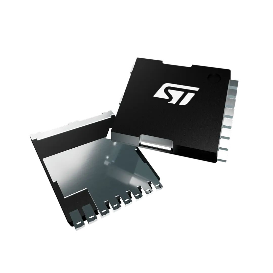
Cooler operation also improves reliability and life cycle, which means that the system tends to last longer and requires less servicing. Lower energy consumption over the product life cycle adds to the savings. Together, these effects reduce the cost of building and operating the system, and they are a large part of why GaN deserves its place in a design.
Where 700 V & 100V PowerGaN FitsThese benefits are not tied to a single product type. The same value higher efficiency, greater density, and lower total cost) extends across a broad range of designs, including AC-DC and DC-DC power supplies, USB Type-C adapters and chargers, LED lighting, motor control, AI servers, robotics, industrial systems, and advanced consumer applications such as home appliances, as well as power and energy systems such as solar and storage. The same value also supports the growing power demands of computing and electrification.
Across these areas, priorities differ, but the same three advantages apply. A choice of package options allows a design team to match the device to the power level and board layout of each application. Because the 700 V & 100V PowerGaN family is already in production and available, these benefits can already be built into designs today.
Backed by a Broad PortfolioAdopting a new switching technology is a decision about support as much as about the device itself. Alongside the 700 V and 100 V family, ST brings decades of power semiconductor experience, a broad product portfolio, a reliable supply chain, and strong technical support. For a team that works with GaN for the first time, that combination reduces the risk of the transition and shortens the path from an idea to a working design. It is part of what makes the value of PowerGaN practical rather than theoretical.
Why GaN, And Why NowGaN power transistors provide higher efficiency, greater power density, and lower system cost for power conversion. The new 700 V and 100 V PowerGaN family makes these benefits available to mainstream designs. For a design team that is considering the move to GaN, the technology has reached the point at which its advantages are practical today rather than promised for tomorrow.
The post GaN Power transistors: What 700 V and 100 V PowerGaN Bring to Power-Supply Design appeared first on ELE Times.
RFID with RC522: Radio-Frequency Identification with Arduino
Let’s get to know and learn how to use a board for RF tag identification, easily paired with Arduino.
We have covered radio-frequency identification, better known as RFID, several times before; for example, in issue no. 254 we dedicated an in-depth look at it with a thorough theoretical introduction and some usage examples based on the RFID PN522 module, accompanied by the ever-present Arduino board. In this article, we pick up the discussion again by experimenting with another module, the RFID-RC522, based on the MFRC522 chip produced by NXP (the datasheet is available at the web link https://www.nxp.com/docs/en/data-sheet/MFRC522.pdf).
The RFID-RC522 moduleThe MFRC522 is a highly integrated RFID reader/writer for contactless communication at 13.56 MHz, supporting the ISO/IEC14443A/MIFARE and NTAG standards.
The transmitter inside the MFRC522 can drive an antenna designed to communicate with cards and transponders without additional active circuits. The internal receiver can efficiently demodulate and decode signals from cards and transponders compatible with the standards listed above.
The MFRC522 supports the MF1xxS20, MF1xxS70, and MF1xxS50 models. It also supports contactless communication with MIFARE transfer rates up to 848 kB (kiloBaud) in bidirectional mode.
The MFRC522 is compatible with all variants of the MIFARE identification protocols MIFARE Mini, MIFARE 1K, MIFARE 4K, MIFARE Ultralight, MIFARE DESFire EV1, and MIFARE Plus RF, grouped under the generic term MIFARE.
Below we summarize the main technical features of the module:
- analog circuit to demodulate and decode responses;
- buffered drivers for connecting an antenna with a reduced number of external components;
- supports ISO/IEC 14443 A/MIFARE and NTAG;
- typical operating distance in read/write mode up to 50 mm depending on antenna size and tuning;
- supports MF1xxS20, MF1xxS70, and MF1xxS50 encryption in read/write mode;
- supports ISO/IEC 14443 with high transfer rate communication up to 848 kbaud;
- supports MFIN/MFOUT;
- additional internal power supply to the smart card IC connected via MFIN/MFOUT;
- supported host interfaces: SPI up to 10 Mbit/s, I²C-Bus up to 400 kBd in Fast mode, up to 3400 kBd in High-speed mode, serial UART RS232 up to 1,228.8 kB/s, with voltage levels depending on the pin supply voltage;
- the FIFO buffer manages sending and receiving at 64 bytes;
- flexible interrupt modes;
- hard reset with low-power function;
- software power-down;
- programmable timer;
- supply voltage from 2.5 to 3.3 V;
- programmable I/O pins.
The RFID-RC522 module is detailed in Fig. 1, where you can see all the available connections.
 Fig. 1 The RFID-RC522 module
Since all current libraries for using the module with Arduino reuse the SPI connection, we will focus only on that; Fig. 2 illustrates the connection to make for the subsequent tests with Arduino UNO.
 Fig. 2 RC522_ISP connections
In Table 1 we describe the connections analytically with their signals: on the left are those of the Arduino UNO and on the right the contacts of the RFID-RC522 module with the corresponding wire colors in the diagram in Fig. 2. The IRQ pin of the RFID module should be left unconnected because we do not manage it in this project and do not need it.
 Table 1 Connections between the RFID-RC522 module and Arduino
Of course, you must be very careful, because swapping just two wires will cause the module to fail; another important thing is power: the module requires 3.3 V, and the corresponding pin on Arduino is right next to the 5 V one; a moment of distraction would almost certainly damage the module.
The board (the RFID module used in the project) comes with two 8-pin strip headers (one straight and one at 90°) to solder as you prefer into the appropriate signal holes, an RFID Tag Card, and an RFID keychain Tag for initial testing.
Libraries for RC522Using this module is made easier by the availability of specific libraries, of which we have selected two: the one from Velleman and the one written by Miguel Balboa.
Velleman: it is a minimal library consisting of only two files (RFID.h and RFID.cpp). Once downloaded from the link: https://www.velleman.eu/downloads/29/vma405_library.zip, you need to include it by opening a new sketch with an updated version of the IDE (in our case 1.8.12). Run the command Sketch – Include Library – Add .ZIP Library… and select the .zip file (Fig. 3), then close the IDE; it will be available when you reopen it.
 Fig. 3 Including the vma405 library
Miguel Balboa: this library, much more powerful and articulated, is recommended by the official Arduino website; it is constantly updated, so it is always best to go to the link https://www.arduino.cc/reference/en/libraries/mfrc522/ or directly to the GitHub https://github.com/miguelbalboa/rfid; at the time of writing, the latest version is 1.4.8.
Its inclusion in the IDE is done in the same way as seen before. This library is quite demanding and requires considerable skills in RFID and programming to exploit it, so we only point it out to more experienced readers, while for the test we will see later we will use the one distributed by Velleman.
Functionality testLet’s start with a test to verify the connections and the correct installation of the vma405 library. We have prepared a sketch named “RFID_TAG_CODE”; open it in the IDE and upload it to the Arduino UNO, then open the Serial Monitor, which will show the message “Avvicina un Tag al Modulo” (Bring a Tag close to the Module); at this point, bring the Tag close to the part of the module where the radio wave symbols are silkscreened (Fig. 4).
 Fig. 4 Reading a Tag with the RC522 module
Keep in mind that the module should always be kept away from devices that can generate electric or electromagnetic fields, otherwise it might not work correctly.
The moment the Tag is recognized, the module reads its UID (unique identification code) and displays it on the Serial Monitor, both in decimal and hexadecimal format; in Fig. 5 we can observe the successive reading of two Tags.
 Fig. 5 Reading the UID of two Tags
If after the first identification you bring the same Tag close again, nothing will happen because we have not included an alternative action in the sketch; bringing another Tag close instead will give its UID in both formats.
When this test succeeds, you need to decide which Tag will be the “System Administrator” of the circuit we have prepared for experimenting with this module and note the five decimal numbers that make up its UID. For our example, we will use the first group visible in the figure (197, 5, 190, 35, 93).
Access control projectWith the help of a breadboard and very few other components, let’s now build a circuit to simulate an access control system using RFID technology with our RC522 module.
The sketch we have prepared can be downloaded and is called Access_Control.rar; it consists of two tabs, and the folder obtained from decompressing the file must be placed in the sketch folder of your IDE; the vma405_library must have been installed beforehand.
The idea is a hypothetical access control system, where the acceptance of a Tag is indicated by the alternating on/off of a blue LED, while rejection is represented by a red LED turning on for about 3 seconds.
Authorized Tags are pre-stored in the EEPROM of the Arduino microcontroller; our sketch supports up to three, but they can be increased up to the availability of the EEPROM. Storage only happens with prior authorization from the “System Administrator,” who has an RFID CARD Tag whose UID must be manually entered in the sketch and which, once read by the module, allows other Tags to be brought close to accredit them and store them in the EEPROM.
From this point on, when you bring an authorized tag near the module, the blue LED will turn on or off with each pass, toggling its state. The red LED, on the other hand, will light up for three seconds when someone tries to gain access with an unregistered tag, effectively denying authorization, and then it will turn off.
Before uploading the sketch to the Arduino, you need to open it and assign the corresponding decimal values of the chosen tag’s UID to the five variables dec_code0 through dec_code4 (Fig. 6), replacing the pre-stored values you will find there.
 Fig. 6 Entering the administrator UID in the sketch
At this point you can upload the sketch to the Arduino and then disconnect the USB cable to remove power. Next, move on to building the practical layout shown in Fig. 7, which explains how to connect all the required components.
 Fig. 7 Wiring diagram of the access control
The materials needed to build the project are:
- RFID-RC522 module
- Arduino UNO
- Breadboard with side power rails (red and black, or red and blue)
- 6×6 mm push button
- Red LED
- Blue LED (or another color of your choice)
- 2 resistors of 220 Ohm
- 1 resistor of 10 kOhm
- 5 M-M jumper wires
- 7 M-F jumper wires
- 1 jumper bridge, 3-pin
- 1 jumper bridge, 5-pin
- 1 jumper bridge, 19-pin
- 4 tags, one of which marked as administrator
Note that regarding jumper wires and bridges, we provided the list to replicate our exact practical layout; of course you can make any variation, as long as you correctly make the proposed connections, otherwise the circuit will not work. Above all, be extremely careful not to reverse the power supply (3.3V and GND), otherwise you risk burning the module!
A special note about the breadboard: during our tests we came across a model with the power rails interrupted in the middle section. This was actually clearly indicated by the break in the red and blue silkscreen lines, but since it is unusual, we initially did not notice it. As a result, the RC522 module’s LED still turned on (due to current carried by the signals), but tag reading did not work. We therefore had to add two jumper wires to connect the two rails along their entire length (Fig. 8), i.e., to bridge them.
 Fig. 8 Detail of the connection of the breadboard power rails
Once the circuit is complete on the breadboard and the connections are checked, to begin simply reconnect the USB cable from the PC to the Arduino UNO board. You will see the RC522 module’s red LED light up (but as explained earlier, this does not indicate correct power supply), while the two red and blue LEDs on the breadboard remain off.
Now open the Serial Monitor of the Arduino IDE, and the message “Controllo accessi attivo” will appear. The first operation to perform is to bring the Administrator tag near the module. If everything is in order, the two LEDs will blink simultaneously three times and remain on; the Serial Monitor will also show the message visible in Fig. 9, indicating that Administrator mode is active.
 Fig. 9 Administrator mode
If at first power-up a number other than 0 appears (usually it will be 255), you need to reset the EEPROM. Simply press the push button mounted on the breadboard to achieve the desired result (Fig. 10).
 Fig. 10 EEPROM reset
After the reset, you will exit Administrator mode and the LEDs will turn off. You must pass the Administrator tag again to re-enter, then simply bring the tag you want to authorize near the module to store its UID (Fig. 11).
 Fig. 11 Storing an authorized tag
This operation can be performed for a maximum of three tags; after that, no more can be stored unless you modify the sketch accordingly.
Daily use of the systemAt this point we can observe the circuit’s behavior depending on the type of tag we bring near the RFID reader; there are two possibilities.
Unregistered tag: the red LED turns on for about three seconds, then turns off; authorization is denied.
Registered tag: if the blue LED is off, it turns on, indicating that authorization has been granted; the LED stays on until you pass the same tag or another registered tag, at which point it turns off.
One last curiosity: if you lack other tags to simulate unauthorized access, you can use your own smartphone. If you have a phone with an NFC chip running Android 5.0 or later, simply enable NFC in the settings and then use the smartphone as if it were a tag.
In fact, when you bring it near the module with the chip side facing it, it will be recognized as a tag, but with a peculiarity that prevents its use as an authorized tag: with each new read, the UID turns out to be different from the previous read. This is easily verifiable with the “RFID_TAG_CODE” sketch. So even if you store the chip as authorized, it will not be recognized on subsequent reads.
In some rare cases, the smartphone may need a specific app to function as a tag. Simply download “NFC Tools” from the Play Store and leave it active, without doing anything else.
ConclusionsWe end this article with a suggestion: as you can easily imagine, this project can be expanded by adding, for example, a relay driven by the same pin as the blue LED, which would allow you to activate an actuator such as an electric lock. The only limits are those of your imagination.
Naturally, the greater the complexity of the expansion, the more variations and implementations you will need to make to the sketch, but it will all be a useful programming exercise that will increase your skills and give you great satisfaction.
The post RFID with RC522: Radio-Frequency Identification with Arduino appeared first on Open Electronics.
RFID with RC522: Radio-Frequency Identification with Arduino
Let’s get to know and learn how to use a board for RF tag identification, easily paired with Arduino.
We have covered radio-frequency identification, better known as RFID, several times before; for example, in issue no. 254 we dedicated an in-depth look at it with a thorough theoretical introduction and some usage examples based on the RFID PN522 module, accompanied by the ever-present Arduino board. In this article, we pick up the discussion again by experimenting with another module, the RFID-RC522, based on the MFRC522 chip produced by NXP (the datasheet is available at the web link https://www.nxp.com/docs/en/data-sheet/MFRC522.pdf).
The RFID-RC522 moduleThe MFRC522 is a highly integrated RFID reader/writer for contactless communication at 13.56 MHz, supporting the ISO/IEC14443A/MIFARE and NTAG standards.
The transmitter inside the MFRC522 can drive an antenna designed to communicate with cards and transponders without additional active circuits. The internal receiver can efficiently demodulate and decode signals from cards and transponders compatible with the standards listed above.
The MFRC522 supports the MF1xxS20, MF1xxS70, and MF1xxS50 models. It also supports contactless communication with MIFARE transfer rates up to 848 kB (kiloBaud) in bidirectional mode.
The MFRC522 is compatible with all variants of the MIFARE identification protocols MIFARE Mini, MIFARE 1K, MIFARE 4K, MIFARE Ultralight, MIFARE DESFire EV1, and MIFARE Plus RF, grouped under the generic term MIFARE.
Below we summarize the main technical features of the module:
- analog circuit to demodulate and decode responses;
- buffered drivers for connecting an antenna with a reduced number of external components;
- supports ISO/IEC 14443 A/MIFARE and NTAG;
- typical operating distance in read/write mode up to 50 mm depending on antenna size and tuning;
- supports MF1xxS20, MF1xxS70, and MF1xxS50 encryption in read/write mode;
- supports ISO/IEC 14443 with high transfer rate communication up to 848 kbaud;
- supports MFIN/MFOUT;
- additional internal power supply to the smart card IC connected via MFIN/MFOUT;
- supported host interfaces: SPI up to 10 Mbit/s, I²C-Bus up to 400 kBd in Fast mode, up to 3400 kBd in High-speed mode, serial UART RS232 up to 1,228.8 kB/s, with voltage levels depending on the pin supply voltage;
- the FIFO buffer manages sending and receiving at 64 bytes;
- flexible interrupt modes;
- hard reset with low-power function;
- software power-down;
- programmable timer;
- supply voltage from 2.5 to 3.3 V;
- programmable I/O pins.
The RFID-RC522 module is detailed in Fig. 1, where you can see all the available connections.
Fig. 1 The RFID-RC522 module
Since all current libraries for using the module with Arduino reuse the SPI connection, we will focus only on that; Fig. 2 illustrates the connection to make for the subsequent tests with Arduino UNO.
Fig. 2 RC522_ISP connections
In Table 1 we describe the connections analytically with their signals: on the left are those of the Arduino UNO and on the right the contacts of the RFID-RC522 module with the corresponding wire colors in the diagram in Fig. 2. The IRQ pin of the RFID module should be left unconnected because we do not manage it in this project and do not need it.
Table 1 Connections between the RFID-RC522 module and Arduino
Of course, you must be very careful, because swapping just two wires will cause the module to fail; another important thing is power: the module requires 3.3 V, and the corresponding pin on Arduino is right next to the 5 V one; a moment of distraction would almost certainly damage the module.
The board (the RFID module used in the project) comes with two 8-pin strip headers (one straight and one at 90°) to solder as you prefer into the appropriate signal holes, an RFID Tag Card, and an RFID keychain Tag for initial testing.
Libraries for RC522Using this module is made easier by the availability of specific libraries, of which we have selected two: the one from Velleman and the one written by Miguel Balboa.
Velleman: it is a minimal library consisting of only two files (RFID.h and RFID.cpp). Once downloaded from the link: https://www.velleman.eu/downloads/29/vma405_library.zip, you need to include it by opening a new sketch with an updated version of the IDE (in our case 1.8.12). Run the command Sketch – Include Library – Add .ZIP Library… and select the .zip file (Fig. 3), then close the IDE; it will be available when you reopen it.
Fig. 3 Including the vma405 library
Miguel Balboa: this library, much more powerful and articulated, is recommended by the official Arduino website; it is constantly updated, so it is always best to go to the link https://www.arduino.cc/reference/en/libraries/mfrc522/ or directly to the GitHub https://github.com/miguelbalboa/rfid; at the time of writing, the latest version is 1.4.8.
Its inclusion in the IDE is done in the same way as seen before. This library is quite demanding and requires considerable skills in RFID and programming to exploit it, so we only point it out to more experienced readers, while for the test we will see later we will use the one distributed by Velleman.
Functionality testLet’s start with a test to verify the connections and the correct installation of the vma405 library. We have prepared a sketch named “RFID_TAG_CODE”; open it in the IDE and upload it to the Arduino UNO, then open the Serial Monitor, which will show the message “Avvicina un Tag al Modulo” (Bring a Tag close to the Module); at this point, bring the Tag close to the part of the module where the radio wave symbols are silkscreened (Fig. 4).
Fig. 4 Reading a Tag with the RC522 module
Keep in mind that the module should always be kept away from devices that can generate electric or electromagnetic fields, otherwise it might not work correctly.
The moment the Tag is recognized, the module reads its UID (unique identification code) and displays it on the Serial Monitor, both in decimal and hexadecimal format; in Fig. 5 we can observe the successive reading of two Tags.
Fig. 5 Reading the UID of two Tags
If after the first identification you bring the same Tag close again, nothing will happen because we have not included an alternative action in the sketch; bringing another Tag close instead will give its UID in both formats.
When this test succeeds, you need to decide which Tag will be the “System Administrator” of the circuit we have prepared for experimenting with this module and note the five decimal numbers that make up its UID. For our example, we will use the first group visible in the figure (197, 5, 190, 35, 93).
Access control projectWith the help of a breadboard and very few other components, let’s now build a circuit to simulate an access control system using RFID technology with our RC522 module.
The sketch we have prepared can be downloaded and is called Access_Control.rar; it consists of two tabs, and the folder obtained from decompressing the file must be placed in the sketch folder of your IDE; the vma405_library must have been installed beforehand.
The idea is a hypothetical access control system, where the acceptance of a Tag is indicated by the alternating on/off of a blue LED, while rejection is represented by a red LED turning on for about 3 seconds.
Authorized Tags are pre-stored in the EEPROM of the Arduino microcontroller; our sketch supports up to three, but they can be increased up to the availability of the EEPROM. Storage only happens with prior authorization from the “System Administrator,” who has an RFID CARD Tag whose UID must be manually entered in the sketch and which, once read by the module, allows other Tags to be brought close to accredit them and store them in the EEPROM.
From this point on, when you bring an authorized tag near the module, the blue LED will turn on or off with each pass, toggling its state. The red LED, on the other hand, will light up for three seconds when someone tries to gain access with an unregistered tag, effectively denying authorization, and then it will turn off.
Before uploading the sketch to the Arduino, you need to open it and assign the corresponding decimal values of the chosen tag’s UID to the five variables dec_code0 through dec_code4 (Fig. 6), replacing the pre-stored values you will find there.
Fig. 6 Entering the administrator UID in the sketch
At this point you can upload the sketch to the Arduino and then disconnect the USB cable to remove power. Next, move on to building the practical layout shown in Fig. 7, which explains how to connect all the required components.
Fig. 7 Wiring diagram of the access control
The materials needed to build the project are:
- RFID-RC522 module
- Arduino UNO
- Breadboard with side power rails (red and black, or red and blue)
- 6×6 mm push button
- Red LED
- Blue LED (or another color of your choice)
- 2 resistors of 220 Ohm
- 1 resistor of 10 kOhm
- 5 M-M jumper wires
- 7 M-F jumper wires
- 1 jumper bridge, 3-pin
- 1 jumper bridge, 5-pin
- 1 jumper bridge, 19-pin
- 4 tags, one of which marked as administrator
Note that regarding jumper wires and bridges, we provided the list to replicate our exact practical layout; of course you can make any variation, as long as you correctly make the proposed connections, otherwise the circuit will not work. Above all, be extremely careful not to reverse the power supply (3.3V and GND), otherwise you risk burning the module!
A special note about the breadboard: during our tests we came across a model with the power rails interrupted in the middle section. This was actually clearly indicated by the break in the red and blue silkscreen lines, but since it is unusual, we initially did not notice it. As a result, the RC522 module’s LED still turned on (due to current carried by the signals), but tag reading did not work. We therefore had to add two jumper wires to connect the two rails along their entire length (Fig. 8), i.e., to bridge them.
Fig. 8 Detail of the connection of the breadboard power rails
Once the circuit is complete on the breadboard and the connections are checked, to begin simply reconnect the USB cable from the PC to the Arduino UNO board. You will see the RC522 module’s red LED light up (but as explained earlier, this does not indicate correct power supply), while the two red and blue LEDs on the breadboard remain off.
Now open the Serial Monitor of the Arduino IDE, and the message “Controllo accessi attivo” will appear. The first operation to perform is to bring the Administrator tag near the module. If everything is in order, the two LEDs will blink simultaneously three times and remain on; the Serial Monitor will also show the message visible in Fig. 9, indicating that Administrator mode is active.
Fig. 9 Administrator mode
If at first power-up a number other than 0 appears (usually it will be 255), you need to reset the EEPROM. Simply press the push button mounted on the breadboard to achieve the desired result (Fig. 10).
Fig. 10 EEPROM reset
After the reset, you will exit Administrator mode and the LEDs will turn off. You must pass the Administrator tag again to re-enter, then simply bring the tag you want to authorize near the module to store its UID (Fig. 11).
Fig. 11 Storing an authorized tag
This operation can be performed for a maximum of three tags; after that, no more can be stored unless you modify the sketch accordingly.
Daily use of the systemAt this point we can observe the circuit’s behavior depending on the type of tag we bring near the RFID reader; there are two possibilities.
Unregistered tag: the red LED turns on for about three seconds, then turns off; authorization is denied.
Registered tag: if the blue LED is off, it turns on, indicating that authorization has been granted; the LED stays on until you pass the same tag or another registered tag, at which point it turns off.
One last curiosity: if you lack other tags to simulate unauthorized access, you can use your own smartphone. If you have a phone with an NFC chip running Android 5.0 or later, simply enable NFC in the settings and then use the smartphone as if it were a tag.
In fact, when you bring it near the module with the chip side facing it, it will be recognized as a tag, but with a peculiarity that prevents its use as an authorized tag: with each new read, the UID turns out to be different from the previous read. This is easily verifiable with the “RFID_TAG_CODE” sketch. So even if you store the chip as authorized, it will not be recognized on subsequent reads.
In some rare cases, the smartphone may need a specific app to function as a tag. Simply download “NFC Tools” from the Play Store and leave it active, without doing anything else.
ConclusionsWe end this article with a suggestion: as you can easily imagine, this project can be expanded by adding, for example, a relay driven by the same pin as the blue LED, which would allow you to activate an actuator such as an electric lock. The only limits are those of your imagination.
Naturally, the greater the complexity of the expansion, the more variations and implementations you will need to make to the sketch, but it will all be a useful programming exercise that will increase your skills and give you great satisfaction.
The post RFID with RC522: Radio-Frequency Identification with Arduino appeared first on Open Electronics.
Q2 smartphone production down just 8% year-on-year, to 275 million units
From Silicon to Scale: Aheesa Signs Packaging MoU with Optilink Networks
Aheesa Digital Innovations, a DLI-scheme backed fabless semiconductor company headquartered in Chennai, has signed a Memorandum of Understanding (MoU) with Optilink Networks Pvt. Ltd., onboarding the company as its packaging partner for VIHAAN-I, Aheesa’s indigenous RISC-V broadband networking System-on-Chip (SoC). The partnership marks another step towards commercialising VIHAAN-I, strengthening the pathway from indigenous chip design and silicon validation to packaging, distribution and market deployment.
The partnership brings together two complementary parts of the broadband technology ecosystem. Optilink has supported the VIHAAN-I journey through testing, validation and engineering support, with its in-house capabilities across product design, firmware development and hardware integration. Under the MoU, Optilink will support end-to-end product development from prototyping to packaging, while the companies work towards developing, qualifying and commercialising ONT/CPE products based on the VIHAAN-I chipset. The collaboration is aimed at delivering solutions that are cost-efficient and comply with Indian and global standards, while accelerating commercialisation through Optilink’s engineering and manufacturing expertise.
This further advances Aheesa’s ambition to establish itself as a semiconductor design house with a portfolio of Indian-designed chips serving both domestic and global markets. With design, silicon validation, packaging and distribution capabilities progressively coming together, Aheesa is now leaping towards commercial deployment in early 2027.
The partnership comes in a landmark year for Aheesa. VIHAAN-I achieved tape-out on Republic Day 2026, followed by Aheesa securing investment from the Tamil Nadu Infrastructure Fund Management Corporation (TNIFMC) through the Tamil Nadu Emerging Sector Seed Fund. On this Independence Day, the chip achieved first-pass silicon success on its very first attempt.
Commenting on the partnership, Sridharan Mani, Founder and CEO, Aheesa Digital Innovations, said, “Building a chip is only half the journey as the real test is turning that silicon into a product people can use. No semiconductor ecosystem thrives on the strength of one player alone; it takes multiple partners, each doing their part, to carry a design to the consumer and make this sector succeed. With Optilink joining us for packaging, VIHAAN-I takes a step closer to that reality. We have spent years estabilishing that world-class semiconductor design can happen in India. Now with Optilink, we’re building the pathway to take it from systems to scale.”
Devchand Haria, Managing Director, Optilink Networks Pvt. Ltd said, “At Optilink, we’ve spent close to two decades building the networking hardware that connects Indian homes from fiber access to broadband CPE. Partnering with Aheesa for VIHAAN-I lets us bring that same experience to an Indian-designed chip, taking it from silicon to the products that will actually sit in Indian households. This is exactly the kind of collaboration our sector needs, that is Indian design and Indian manufacturing expertise working together to put homegrown silicon inside the devices people use every day.”
Founded in 2005 and headquartered in Mumbai, Optilink Networks Pvt. Ltd. is an Indian Original Equipment Manufacturer (OEM) that designs, manufactures and distributes IP-based networking hardware, Fiber-to-the-Home (FTTH) solutions and IP Television (IPTV) technologies. Serving ISPs, telecom operators, cable and MSO networks, enterprises and government customers, Optilink has built a strong B2B presence through its channel partners, distributors and system integrators across India.
Aheesa’s work spans indigenous semiconductor and networking technologies across telecom, broadband, cybersecurity and edge computing. This partnership now reflects the wider momentum in India’s semiconductor design ecosystem, now scaling under Semicon 2.0 — the ₹1,27,500 crore programme approved in July 2026 to build a globally competitive supply chain across chip design, manufacturing, packaging and materials. As indigenous designs move from validation towards commercial adoption, it is partnerships like this, pairing Indian chip design with the reach to deploy it, that will help define how homegrown silicon scales.
The post From Silicon to Scale: Aheesa Signs Packaging MoU with Optilink Networks appeared first on ELE Times.
Pages




![[link]](https://i.redd.it/a9r8xszzqcoh1.jpeg)
![[link]](https://i.redd.it/w8u7wjxupaoh1.png)