
Feed aggregator
Акредитація освітніх програм КПІ ім. Ігоря Сікорського 2025/06/10

🏆 10 червня 2025 року відбулося чергове засідання Національного агентства із забезпечення якості вищої освіти (НАЗЯВО). За результатами засідання було прийняте рішення про акредитацію п'яти освітніх програм (ОП) нашого університету за повною процедурою терміном на 5 років!
I weaved 64 bytes of magnetic core memory
 | submitted by /u/AdEast7904 [link] [comments] |
A simulated 100-MHz VFC

Stephen Woodward, a prolific circuit designer with way more than 100 published Design Ideas (DIs), had his “80 MHz VFC with prescaler and preaccumulator” [1] published on October 17, 2024, as a DI on the EDN website.
Upon reading his article, I was eager to simulate it and try to push its operation up to 100 MHz, if possible, while maintaining its basic simplicity and accuracy. However, Stephen Woodward got there before I did [2]! For the record, I had almost finished my design before I saw his latest one on the EDN website.
I won’t discuss the details of the circuit operation because they are so similar to those of the above-referenced DIs. However, there are added features, and the functionality has been tested by simulation.
Wow the engineering world with your unique design: Design Ideas Submission Guide
FeaturesMy voltage-to-frequency converter (VFC) circuit (Figure 1) has a high impedance input stage, it can operate reliably beyond 100 MHz, it can be operated with a single 5.25-V supply (or a single 5-V supply with a few added components), and it has been successfully simulated. Also, adjustments are provided for calibration.
Figure 1 VFC design that operates from 100 kHz to beyond 100 MHz with a single 5.25-V supply, providing square wave outputs at 1/2 and 1/4 the main oscillator frequency.
This circuit provides square wave outputs at one-half and one-fourth the main oscillator frequency. These signals will, in many cases, be more useful than the very narrow oscillator signal, which will be in the 2 ns to 5 ns range.
The NE555 (U8) provides a 500 kHz signal, which drives both a negative voltage generator for a -2.5-V reference and a voltage doubler used to generate a 5.25-V regulated supply that is used when a single 5-V supply is desired. TLA431As are used as programmable Zener diodes, NOT TL431As. Unlike the TL431A, the TLA431A is stable for all values of capacitance connected from the cathode to the anode.
Two adjustments are provided: Both a positive and a negative offset adjustment are provided by R11, and R9 adjusts the gain of the current-to-voltage converter, U2. I suggest using R11 to set the 100-kHz signal with 5 mV applied to the input and using R9 to set the 100-MHz signal with a 5-V input. Repeat this procedure as required to maximize the accuracy of the circuit.
Possible limitationsThis circuit may not give highly accurate operation below 100 kHz because of diode and transistor leakage currents, but I expect it to operate at the lower frequencies at least as well as Woodward’s circuits. Operation down to 1 Hz or 10 Hz is, in my opinion, mostly for bragging rights, and I am not concerned about that.
I expect this VFC to be useful mostly in the 100 kHz to 100 MHz frequency range: a 1 to 1000 span. Minute diode/transistor leakage currents in the nanoamp range and PCB surface leakage may cause linearity inaccuracies at the lower frequencies. The capacitor charging current provided by transistor Q1 is in the several microamps range at 100 kHz; below that, it is in the nanoamp range. Having had some experience with environmental testing, I think it would be difficult to build this circuit so that it would provide accurate operation below 100 kHz in an environment of humidity/temperature of 75%/50oC.
Some detailsWhen simulated with LTspice, the Take Back Half circuit [3] with 1N4148 diodes did not provide acceptable results above about 3.5 MHz when driven by a square wave signal with 2-ns rise/fall times, so I used Schottky barrier diodes instead, which worked well beyond 25 MHz, the maximum frequency seen by the Take Back Half circuit [1,3]. The Schottky diodes have somewhat higher leakage current than the 1N4148s, but the 1N4148 diodes would require the highest frequency signal to be divided down to 3.5 MHz to operate well in this application.
I used two 74LVC1G14s to drive C4, the ramp capacitor, because I was not convinced one of them was rated to continuously drive the peak or rms current required to reset the capacitor when operating at or near 100 MHz. And using a 25-pF capacitor instead of just using parasitic and stray capacitance allows better operation at low frequencies because leakage currents are a smaller percentage of the capacitor charging current. (Obviously, more ramp capacitance requires more charging current.)
The op-ampIf you want to use a different op amp, check the specs to be sure the required supply current is not greater than 3 mA worst case. Also, it must accommodate the necessary 7.75 V with some margin. Critically, the so-called rail-to-rail output must swing to within 100 mV of the positive rail with a 1.3-mA load at the maximum operating temperature.
Be advisedLook at renowned Jim Williams’ second version of his 1 Hz to 100 MHz VFC for more information about the effort required to make his circuit operate well over the full frequency range [4][5]. See reference 5 and look at the notes in Figure 1 and Table 1.
Jim McLucas retired from Hewlett-Packard Company after 30 years working in production engineering and on design and test of analog and digital circuits.
References/Related Content
- 80 MHz VFC with prescaler and preaccumulator
- 100-MHz VFC with TBH current pump
- Take-Back-Half precision diode charge pump
- Designs for High Performance Voltage-to-Frequency Converters
- 1-Hz to 100-MHz VFC features 160-dB dynamic range
The post A simulated 100-MHz VFC appeared first on EDN.
Infineon expands government ID portfolio with SECORA ID V2 and eID-OS for enhanced flexibility and faster time-to-market
Electronic identification (eID) documents are seeing growing demand worldwide as governments push ahead with their digitalization efforts. To meet these rapidly evolving requirements more quickly and flexibly, Infineon Technologies AG has introduced two new solutions: SECORA ID V2 and the eID-OS. These solutions offer local security printers and card manufacturers greater flexibility in selecting the right solution for their specific project requirements, while helping to reduce development time and accelerate deployment.
“Our broad range of solutions is a clear commitment to our customers and their individual, local requirements in the field of ID projects,” says Maurizio Skerlj, Senior Vice President and Product Line Manager for Authentication and Identity Solutions at Infineon Connected Secure Systems. “With our all-in-one solutions, including innovative packaging options such as our coil-on-module technology and our antenna design support, we enable our customers to get their products to market faster, develop a flexible solution to their specific requirements, and realize new applications.”
SECORA ID V2: improved security features and faster transaction speeds
SECORA ID V2 is the successor to the SECORA ID V1 Java Card solution for electronic ID and authentication applications in the public sector. The V2 version of SECORA ID increases transaction speed by up to 80 percent compared to its predecessor. It is based on a 40 nm hardware architecture and can transfer data at speeds of up to 6.8 MBit/s. This enables faster personalization and processing of ID documents and allows for quick and smooth identity checks at borders and security checkpoints. SECORA ID V2 is based on the latest Java Card 3.1 standard and supports biometric match-on-card functions to increase user data protection. Customers benefit from Infineon’s broad applet toolset. It also supports payment tools such as Visa, Mastercard, and Calypso as well as the crypto vision ePasslet Suite. This wide range of applets enables developers to easily integrate and quickly deploy highly customized ID solutions. Furthermore, the sandbox enables the integration of native code without compromising security standards. The SECORA ID V2 platform is Common Criteria EAL6+(high) certified and EMVCo approved.
Infineon eID-OS: Ready-to-use and low operating expenses
Infineon eID-OS is the latest addition to the portfolio of native solutions, combining the latest TEGRION security controller with a native operating system. Designed for basic ID application projects, it offers a performance- and cost-optimized solution with fast time-to-market. The standards-compliant solution is targeting CC EAL 5+ eMRTD (Common Criteria Evaluation Assurance Level for electronic Machine-Readable Travel Document) certification and is housed in advanced packaging technology. It optimizes the development process, enables rapid deployment, and reduces maintenance costs. Featuring a powerful 32-bit CPU, advanced cryptography accelerators, and the robust Integrity Guard 32 security architecture, eID-OS enables fast and secured transactions with processing times of less than 0.5 seconds. Thanks to simplified implementation, personalization, and administration, as well as a secured chain of trust and automatic data size detection, customers benefit from low total cost of ownership. In addition, Infineon’s ultra-thin contactless coil-on-module package supports thinner electronic data pages, reducing document costs and the carbon footprint. The space saved can alternatively be used for an additional security layer, making this solution ideal for modern eID projects.
The post Infineon expands government ID portfolio with SECORA ID V2 and eID-OS for enhanced flexibility and faster time-to-market appeared first on ELE Times.
Arrow Electronics Launches Comprehensive Energy Storage Resource Hub
Arrow Electronics has launched a dedicated online hub offering extensive resources for those seeking to understand the future of energy storage systems.
As the global shift towards renewable energy accelerates, battery energy storage systems (BESS) are becoming critical in revolutionising energy storage and management. BESS technology plays a vital role in integrating solar and wind power, enabling the electrification of vehicles, and providing reliable backup power, ultimately enhancing sustainability and resilience across various sectors.
The new energy storage systems resource page provides access to a range of valuable content, including a webinar on ‘Optimising Energy Storage: The Role of Advanced BMS,’ an informative e-book on BESS, essential design resources, insightful articles exploring key energy storage topics, such as photovoltaic integration and recordings of on-demand webinars, including ‘High-Power SiC MOSFETs Designed to Last.’
Arrow, in collaboration with eInfochips, is driving innovation in the BESS sector by offering leading-edge components, expert engineering support, and dependable supply chain solutions.
The post Arrow Electronics Launches Comprehensive Energy Storage Resource Hub appeared first on ELE Times.
Нове укриття у 18-му корпусі КПІ ім. Ігоря Сікорського

Нещодавно було відкрито ще одне укриття на 150 осіб у корпусі №18, до розробки проєкту якого також долучалися студенти.
КПІ ім. Ігоря Сікорського співпрацюватиме з Асоціацією українських підприємств целюлозно-паперової галузі «УкрПапір»

Партнерство між КПІ ім. Ігоря Сікорського та Асоціацією українських підприємств целюлозно-паперової галузі «УкрПапір» — приклад синергії інтересів промислового виробництва і профільної освіти. Зокрема, на базі Інженерно-хімічного факультету (ІХФ) КПІ ім. Ігоря Сікорського готуватиметься нова генерація фахівців відповідно до викликів і потреб сучасного ринку:
Відкрито меморіальні дошки загиблим студентам і випускникам КПІ ім. Ігоря Сікорського

У навчальних корпусах №7 та №22 КПІ ім. Ігоря Сікорського відкрито меморіальні дошки загиблим студентам і випускникам КПІ ім. Ігоря Сікорського, які віддали своє життя за свободу та незалежність України. На відкритті були присутні представники університету, родичі та побратими загиблих.
STM32 LED Matrix Clock with Temp Sensors
 | Built a wall-mounted box with STM32F103 (CubeMX + HAL). Shows time from DS3231 and temps from two DS18B20 (outside + inside) on a 4x MAX7219 matrix. [link] [comments] |
Chiplet basics: Separating hype from reality

There’s currently a significant buzz within the semiconductor industry around chiplets, bare silicon dies intended to be combined with others into a single packaged device. Companies are beginning to plan for chiplet-based designs, also known as multi-die systems. Yet, there is still uncertainty about what designing chiplet architecture entails, which technologies are ready for use, and what innovations are on the horizon.
Understanding the technology and supporting ecosystem is necessary before chiplets begin to see widespread adoption. As technology continues to emerge, chiplets are a promising solution for many applications, including high-performance computing, AI acceleration, mobile devices, and automotive systems.

Figure 1 Understanding the technology is necessary before chiplets begin to see widespread adoption. Source: Arteris
The rise of chiplets
Until recently, integrated circuits (ICs), application-specific integrated circuits (ASICs), application-specific standard products (ASSPs), and system-on-chip (SoC) devices were monolithic. These devices are built on a single piece of silicon, which is then enclosed in its dedicated package. Depending on its usage, the term chip can refer to either the bare die itself or the final packaged component.
Designing monolithic devices is becoming increasingly cost-prohibitive and harder to scale. The solution is to break the design into several smaller chips, known as chiplets, which are mounted onto a shared base called a substrate. All of this is then enclosed within a single package. This final assembly is a multi-die system.
Building on this foundation, the following use cases illustrate how chiplet architectures are being implemented. Split I/O and logic is a chiplet use case in which the core digital logic is implemented on a leading-edge process node. Meanwhile, I/O functions such as transceivers and memory interfaces are offloaded to chiplets built on older, more cost-effective nodes. This approach, used by some high-end SoC and FPGA manufacturers, helps optimize performance and cost by leveraging the best technology for each function.
A reticle limit partitioning use case implements a design that exceeds the current reticle limit of approximately 850 mm2 and partitions it into multiple dies. For example, Nvidia’s Blackwell B200 graphics processing unit (GPU) utilizes a dual-chiplet design, where each die is approximately 800 mm² in size. A 10 terabytes-per-second link enables them to function as a single GPU.
Homogeneous multi-die architecture integrates multiple identical or functionally similar dies, such as CPUs, GPUs, or NPUs, on a single package or via an ‘interposer’, a connecting layer similar to a PCB but of much higher density and typically made of silicon using lithographic techniques. Each die performs the same or similar tasks and is often fabricated using the same process technology.
This approach enables designers to scale performance and throughput beyond monolithic die designs’ physical and economic limits, mainly as reticle limits of approximately 850 mm² constrain single-die sizes or decreasing yield with increasing die size makes the solution cost-prohibitive.
Functional disaggregation is the approach most people think of when they hear the word chiplets. This architecture disaggregates a design into multiple heterogeneous dies, where each die is realized at the best node in terms of cost, power, and performance for its specific function.
For example, a radio frequency (RF) die might be implemented using a 28 nm process, analog-to-digital converters (ADCs) and digital-to-analog converters (DACs) could be realized in a 16 nm process, and the core digital logic might be fabricated using a 3 nm process. Large SRAMs may be implemented in 7 nm or 5 nm, as RAM has not scaled significantly in finer geometries.
The good news
There are multiple reasons why companies are planning to transition or have transitioned to chiplet-based architectures. These include the following:
- Chiplets can build larger designs than are possible on a single die.
- Higher yields from smaller dies reduce overall manufacturing costs.
- Chiplets can mix and match best-in-class processing elements, such as CPUs, GPUs, NPUs, and other hardware accelerators, along with in-package memories and external interface and memory controllers.
- Multi-die systems may feature arrays of homogeneous processing elements to provide scalability, or collections of heterogeneous elements to implement each function using the most advantageous process.
- Modular chiplet-based architectures facilitate platform-based design coupled with design reuse.

Figure 2 There are multiple drivers pushing semiconductor companies toward chiplet architectures. Source: Arteris
The ecosystem still needs to evolve
While the benefits are clear, several challenges must be addressed before chiplet-based architectures can achieve widespread adoption. While standards like PCIe are established, die-to-die (D2D) communication standards like UCIe and CXL continue to emerge, and ecosystem adoption remains uneven. Meanwhile, integrating different chiplets under a common set of standards is still a developing process, complicating efforts to build interoperable systems.
Effective D2D communication must also deliver low latency and high bandwidth across varied physical interfaces. Register maps and address spaces, once confined to a single die, now need to extend across all chiplets forming the design. Coherency protocols such as AMBA CHI must also span multiple dies, making system-level integration and verification a significant hurdle.
To understand the long-term vision for chiplet-based systems, it helps first to consider how today’s board-level designs are typically implemented. This usually involves the design team selecting off-the-shelf components from distributors like Avnet, Arrow, DigiKey, Mouser, and others. These components all support well-defined industry-standard interfaces, including I2C, SPI, and MIPI, allowing them to be easily connected and integrated.
In today’s SoC design approach, a monolithic IC is typically developed by licensing soft intellectual property (IP) functional blocks from multiple trusted third-party vendors. The team will also create one or more proprietary IPs to distinguish and differentiate their device from competitive offerings. All these soft IPs are subsequently integrated, verified, and implemented onto the semiconductor die.
The long-term goal for chiplet-based designs is an entire chiplet ecosystem. In this case, the design team would select a collection of off-the-shelf chiplets created by trusted third-party vendors and acquired via chiplet distributors rather as board-level designers do today. The chiplets will have been pre-verified with ‘golden’ verification IP that’s trusted industry-wide, enabling seamless integration of pre-designed chiplets without the requirement for them to be verified together prior to tape-out.
The team may also develop one or more proprietary chiplets of their own, utilizing the same verification IP. Unfortunately, this chiplet-based ecosystem and industry-standard specification levels are not expected to become reality for several years. Even with standards such as UCIe, there are many options and variants within the specification, meaning there is no guarantee of interoperability between two different UCIe implementations, even before considering higher-level protocols.
The current state-of-play
Although the chiplet ecosystem is evolving, some companies are already creating multi-die systems. In some cases, this involves large enterprises such as AMD, Intel, and Nvidia, who control all aspects of the development process. Smaller companies may collaborate with two or three others to form their own mini ecosystem. These companies typically leverage the current state-of-play of D2D interconnect standards like UCIe but often implement their own protocols on top and verify all chiplets together prior to tape-out.
Many electronic design automation (EDA) and IP vendors are collaborating to develop standards, tool flows, and crucially VIP. These include companies like Arteris, Cadence, Synopsys, and Arm, as well as RISC-V leaders such as SiFive and Tenstorrent.
Everyone is jumping on the chiplet bandwagon these days. Many are making extravagant claims about the wonders to come, but most are over-promising and under-delivering. While a truly functional chiplet-based ecosystem may still be five to 10 years away, both large and small companies are already creating chiplet-based designs.
 Ashley Stevens, director of product management and marketing at Arteris, is responsible for coherent NoCs and die-to-die interconnects. He has over 35 years of industry experience and previously held roles at Arm, SiFive, and Acorn Computers.
Related Content
- A closer look at Arm’s chiplet game plan
- TSMC, Arm Show 3DIC Made of Chiplets
- Chiplets Get a Formal Standard with UCIe 1.0
- How the Worlds of Chiplets and Packaging Intertwine
- Imec’s Van den hove: Moving to Chiplets to Extend Moore’s Law
The post Chiplet basics: Separating hype from reality appeared first on EDN.
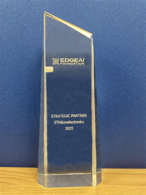
Edge AI Foundation: powering the next wave of intelligence at the edge
Author: STMicroelectronics
From cloud-first to edge-ready: why AI needs to evolveArtificial Intelligence (AI) has come a long way in the last decade. While cloud-based infrastructure enabled massive leaps in AI capabilities, it also introduced new challenges, such as latency, energy consumption, and privacy concerns. In response, companies and researchers started focusing on edge AI, where data is processed locally on embedded systems such as sensors and microcontrollers. The Edge AI Foundation (formerly known as TinyML) has been a driver in this transition since its creation in 2018 by bringing together industry leaders and innovators to make AI smarter, faster, and more pervasive at scale.
The evolution of AI developmentArtificial Intelligence started to attract mainstream attention around 2012, when deep learning models achieved remarkable success in areas like image recognition, speech processing, and translation. The emergence of cloud computing drove these advancements, offering the computational resources required to train complex models on large datasets.
Over the next several years, companies invested heavily in cloud-based AI infrastructure, using high-performance GPUs to develop ever-larger models, including the early versions of generative AI. By 2017, AI was firmly embedded in cloud services offered by major tech providers.
However, as adoption grew, so did concerns about latency, bandwidth, privacy, and the high energy costs of transmitting and processing data remotely. These limitations became more pronounced as AI moved into latency-critical applications like autonomous systems, wearable tech, and industrial automation. The result was a gradual understanding that not all AI needs to live in the cloud and that many use cases could benefit from performing AI computations locally, closer to the data source. This awareness laid the foundation for the next significant shift: AI at the edge.
Why edge AI is the next big stepAs AI becomes more integrated into everyday life, the need for fast, private, and energy-efficient processing is growing. Traditional cloud-based AI requires data to be sent to remote servers for analysis and decision-making, introducing latency, increasing energy use, and raising privacy concerns. Edge AI solves these challenges by enabling intelligent processing directly on local devices, such as sensors, microcontrollers, and other embedded processing solutions. This eliminates or reduces the need to constantly connect to the cloud.
Thanks to key advancements like the STM32 microcontroller family and ST’s intelligent MEMS sensors portfolio, from inertial measurements units to biosensors, edge AI is no longer experimental; it’s a pervasive solution. Edge AI technologies empower devices to execute neural network inference locally, facilitating tasks such as anomaly detection, pose estimation, gesture recognition, environmental monitoring, and more. These functions are crucial in fields like industrial automation, healthcare, and innovative consumer products, where low latency, robust security, and minimal energy use are essential.
Among these innovations it is worth mentioning the STM32N6 series, ST’s first microcontroller family to integrate the Neural-ART Accelerator, a proprietary Neural Processing Unit (NPU). This NPU accelerates AI inference workloads directly on the MCU, drastically reducing latency, power consumption and off-loading the CPU for AI computing. Designed for demanding edge applications, the STM32N6 combines advanced performance, a unique video acquisition pipeline, and unprecedented energy efficiency with the flexibility of the STM32 programming ecosystem.
The Edge AI Foundation: a community driving changeThe Edge AI Foundation is a strategic think tank committed to advancing edge AI across sectors. It hosts global conferences, such as annual events in Europe, the U.S., and Asia, connecting academia and industry. As a non-profit, the Foundation doesn’t promote specific products; instead, it fosters knowledge exchange, networking, joint research, and alignment on frameworks and tools.
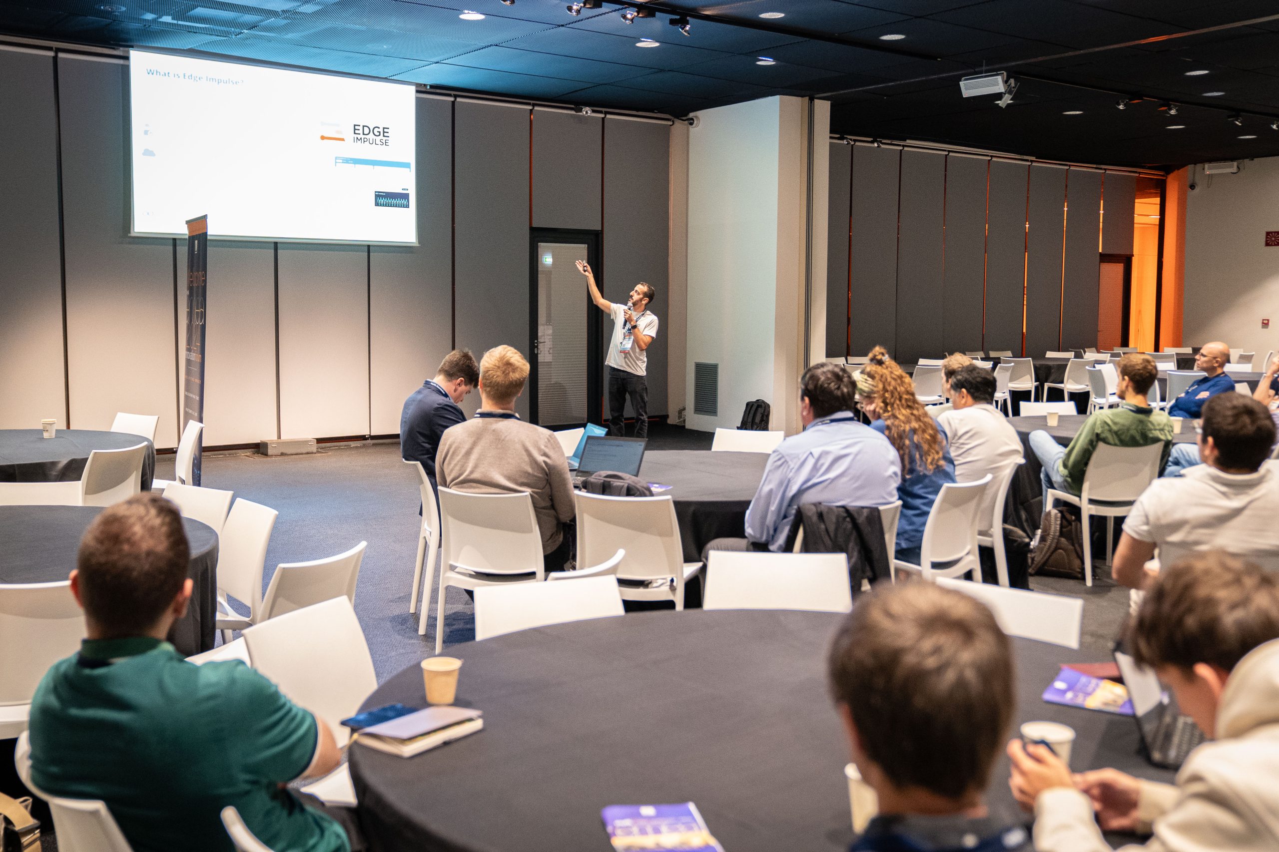 Knowledge exchange at TinyML EMEA 2024
The journey of the Edge AI Foundation began in 2018 with the establishment of the TinyML Foundation, a collaborative community initiated by industry leaders such as Google, ARM, and STMicroelectronics.
The Foundation’s goal was to create a community of experts who could prove that machine learning could be executed even on ultralow-power devices (under 1mW), unlocking a new class of applications that operate independently of cloud infrastructure. This first step addressed the growing demand for real-time, energy-efficient, and privacy-preserving AI applications in areas like wearables, smart homes, and industrial IoT. And it was relatively quick to achieve.
As the field matured, the scope of applications expanded beyond simple models to encompass more complex tasks, such as generative and agentic AI, computer vision, and natural language processing, all executed at the edge. Following this evolution, in 2024 the TinyML Foundation rebranded itself as the Edge AI Foundation, reconfirming its commitment to advancing AI technologies that operate at the network’s edge.
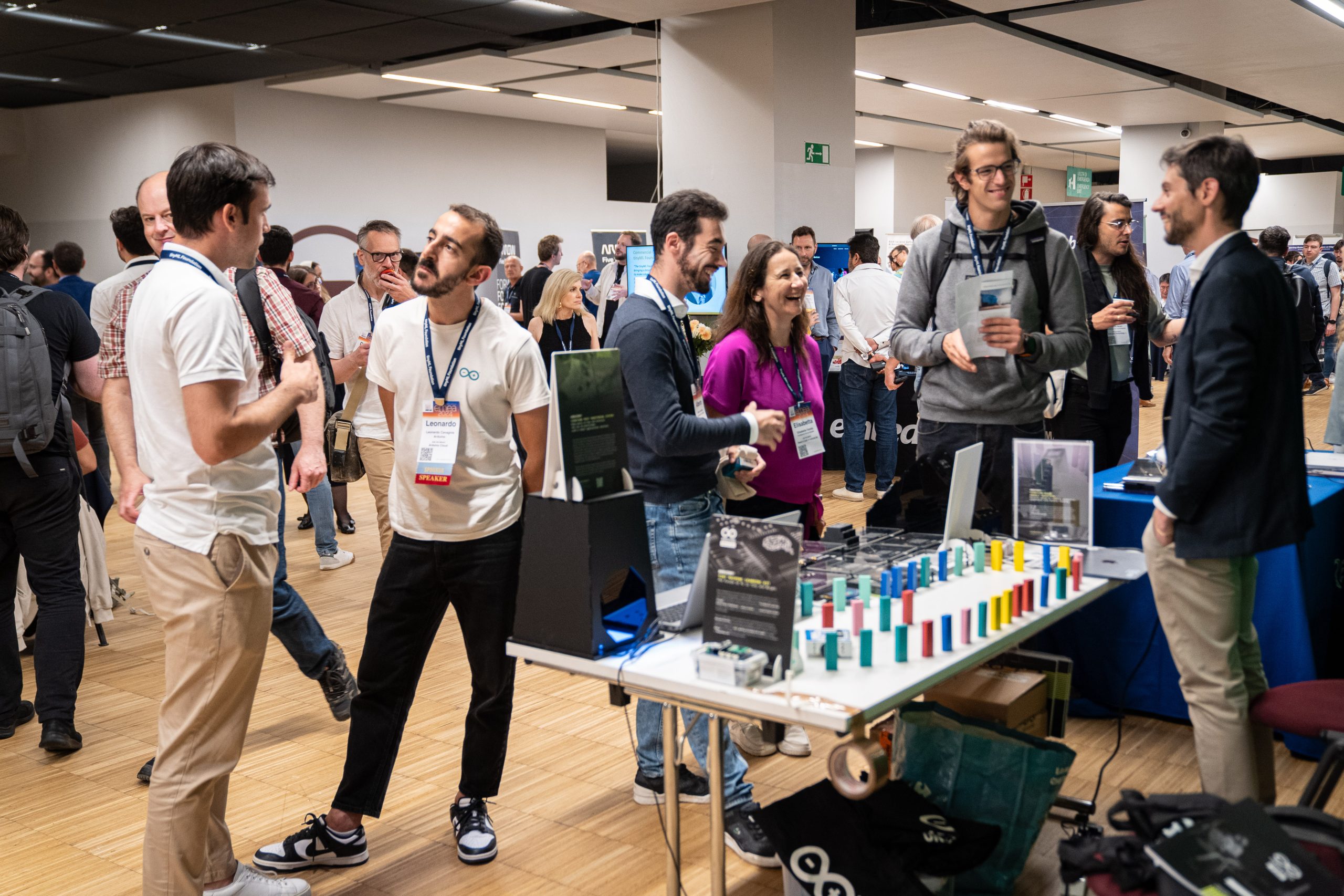 Participants at TinyML EMEA 2024
Today, the Edge AI Foundation brings together a diverse community of researchers, developers, business leaders, and policymakers to address the challenges and opportunities in deploying AI at the edge. The foundation aims to make edge AI technology accessible and impactful for all. To achieve this mission, the Foundation has launched several initiatives:
- Edge AI Working Groups: focus groups on Generative AI, Blueprints, Dataset and Benchmarking, Neuromorphic and Marketing.
- Edge AI Labs: a platform providing access to high-quality datasets, models, and code to accelerate edge AI research and development.
- Edge AIP (Academia & Industry Partnership): a program promoting collaboration between industry partners and academic institutions to develop educational materials, certification programs, and scholarship opportunities.
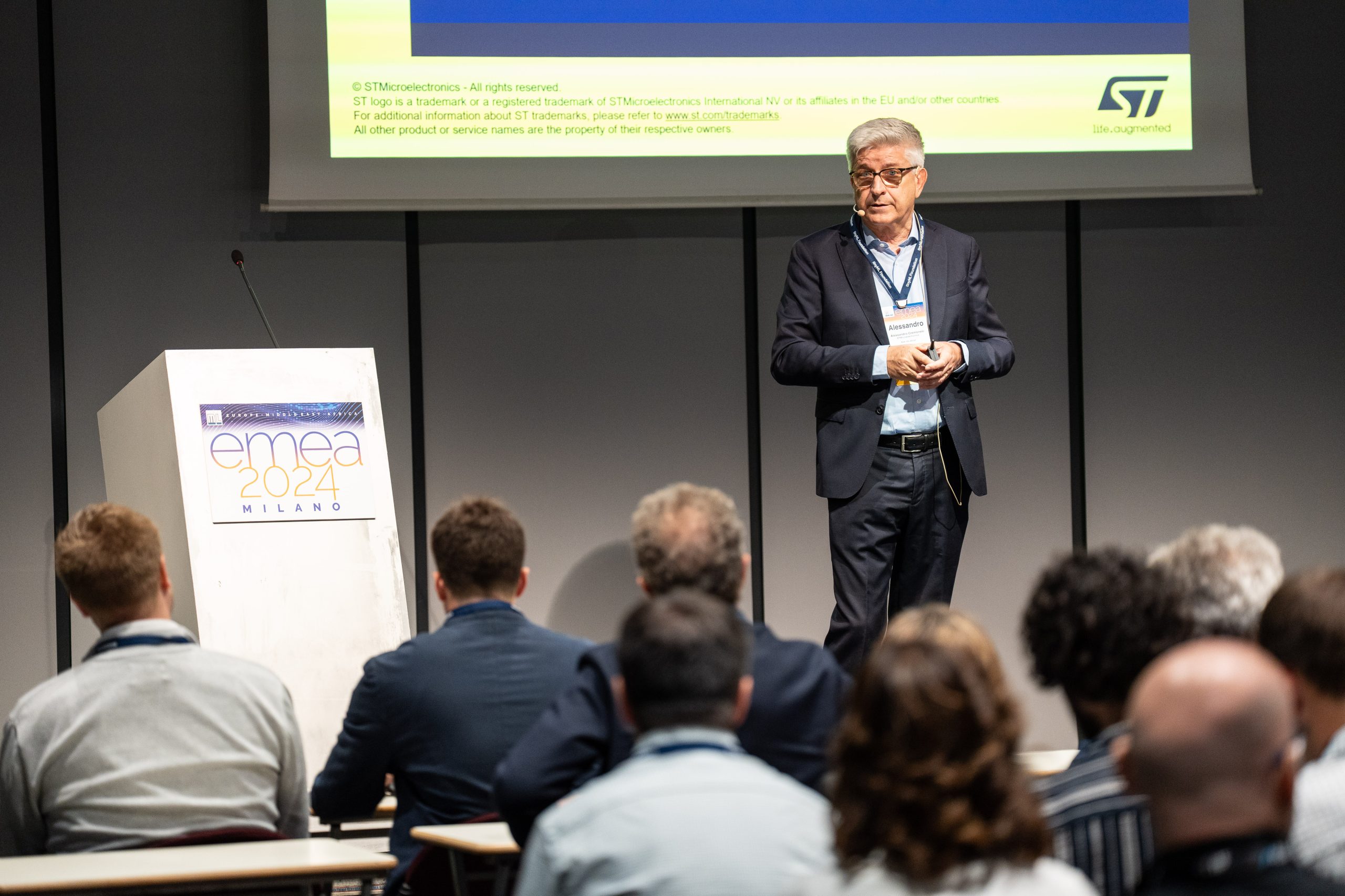 Alessandro Cremonesi (ST Chief Innovation Officer & Executive Vice President General Manager System Research and Applications) at TinyML EMEA 2024
STMicroelectronics began collaborating with the Edge AI Foundation in 2018. This relationship started after ST demonstrated its STM32Cube.AI pre-production tool version at the CES event in Las Vegas. This seminal project led to an invitation by Pete Warden (past TensorFlow Lite tech lead at Google) to the first TinyML US Forum in early 2019. ST showcased live AI demonstrations of its standard STM32 microcontrollers on that occasion.
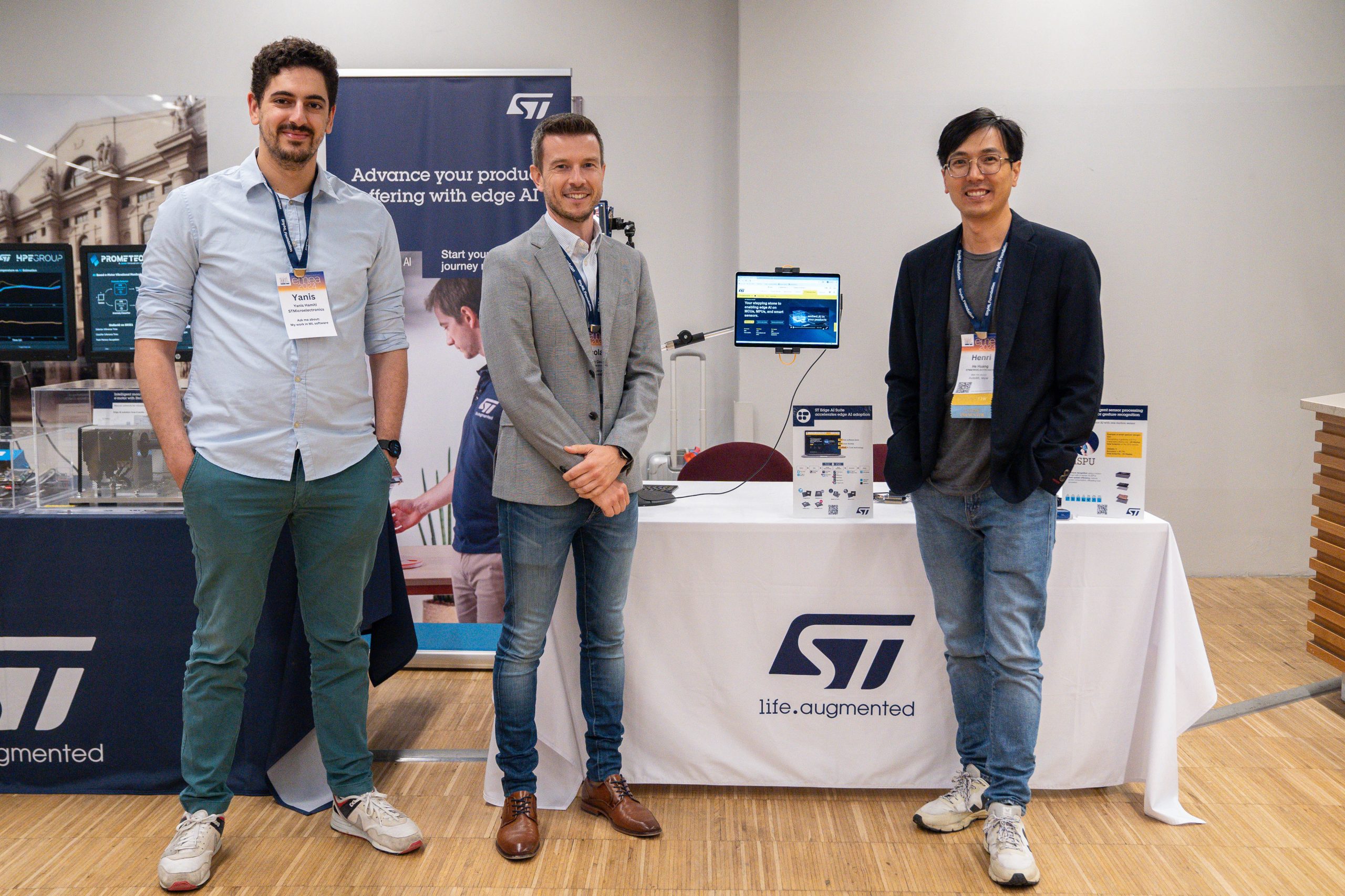 ST demo owners (Yanis Hamiti, Nicolas Gaude and He Huang) at TinyML EMEA 2024
Nowadays, as a Strategic Leader Sponsor, ST participates in and lead working groups, contributes to event programming, and engages in the Foundation’s governance.
For example, Danilo Pau (Technical Director, IEEE, AAIA and ST Fellow in System Research) chairs the Foundation’s Gen EDGE AI working group, organizing forums, producing white papers and initiating research projects leveraging existing ST AI products. Additionally, Giuseppe Desoli (ST’s Company Fellow, SRA Chief architect, Senior Director of Artificial Intelligence & Embedded Architectures) was appointed a Board member in 2025.
This participation supports the promotion of ST’s edge AI solutions, including its portfolio of AI-enabled microcontrollers, such as STM32 general-purpose MCUs and Stellar automotive MCUs, along with sensors and the comprehensive software tools ecosystem that make up the ST Edge AI Suite, while also building a network of authorized partners.
From smart devices to autonomous agentsEdge AI is expected to power the next generation of intelligent agents and systems capable of reasoning, planning, adapting and acting. We are already starting to see early use cases: AI-powered thermostats that learn user behavior, voice assistants that operate offline, intelligent voice transcriptors and humanoid robots that help with manufacturing tasks. In the future, these autonomous systems could help manage entire smart buildings, improve energy efficiency, or support industrial automation, all without needing a constant connection to the cloud.
To support this shift, edge AI platforms need to be highly efficient in both energy and performance. ST is enabling customers to implement edge AI daily thanks to innovations that facilitate edge AI on a broad range of STM32 microcontroller family, Microcontrollers integrating an NPU, and intelligent MEMS sensors with two technologies: the intelligent Sensor Processing Unit (ISPU) and machine learning core (MLC).
As an active contributor to the Edge AI Foundation, ST will continue to influence this community, enabling faster innovation and more sustainable technology at the edge.
The post Edge AI Foundation: powering the next wave of intelligence at the edge appeared first on ELE Times.
eevBLAB 129 - WARNING: New Youtube Creator Channel Hijack Scam
I'm working on a project to help a visually impaired student of mine build circuits. Here's the prototype in action on an Atari Punk Console
 | While there are lots of nice solutions out there for accessible circuit building (Tronic boards, Little Bits, Snap Circuits, etc) most of these are kind of closed ecosystems, with components permanently mounted in modules. What I needed was a way for her to be able to use bog standard components, but not have to deal with fiddly connections. I'll add some more pictures of the individual boards in the comments. Feedback and suggestions are very welcome. [link] [comments] |
Custom Digital Watch DIY
 | This is just a prototype. in future it will be better for example we can get rid of square thing, polish metal so it looks like actual metal. and reduce the height. final one I also want to use a stm32u5 I spent a lot of months doing this [link] [comments] |
Weekly discussion, complaint, and rant thread
Open to anything, including discussions, complaints, and rants.
Sub rules do not apply, so don't bother reporting incivility, off-topic, or spam.
Reddit-wide rules do apply.
To see the newest posts, sort the comments by "new" (instead of "best" or "top").
[link] [comments]
Think that I have enough resistors for now.
 | Theres well over 6k resistors in this drawer, think that it's enough? [link] [comments] |
Time-to-digital conversion for space applications
 What is a TDC?
A time-to-digital converter (TDC) is like a stopwatch measuring the elapsed interval between two events with picosecond precision, converting this into a digital value for post-processing. Many space applications require time-of-flight measurements to calculate distance, delay, or velocity. For example, an in-space servicing, assembly, and manufacturing (ISAM) spacecraft needs to determine precisely the relative location of debris before initiating rendezvous and retrieval operations. Similarly, space-domain awareness must understand the proximity and trajectory of other orbiting objects to assess any potential threat.
A TDC receives two inputs: a start signal (or edge) to mark the beginning of the time interval to be measured, and a stop pulse. The delay between these is converted to a digital number for post-processing. Different architectures are typically used to implement the logic, e.g., counters, delay lines, or a time amplifier.
Time-to-digital conversion is a technique used in space-based LiDAR systems to measure the time taken for a light pulse to travel to and from an object to calculate its distance. A LiDAR emits a laser pulse towards a target, which reflects off the latter’s surface, returning to the sensor. The TDC starts counting when the pulse is transmitted, stops when it is detected by the receiver, and using the speed of light, the distance is calculated as:
![]()
where c is the speed of light and t is the time-of-flight.
TDC in LiDARFor example, LiDAR is used by some Earth-Observation operators to measure altitude and surface changes over time, to, for example, monitor vegetation height, ice sheet or glacier thickness and melt, sea-ice elevation or relative sea level. Spaceborne LiDAR altimetry is capable of centimetre-level vertical precision and is illustrated in Figure 1.
 Figure 1 The use of TDC in space-based LiDAR applications. Source: Rajan Bedi
Similarly, a TDC is used in mass spectroscopy to measure how long it takes ions to travel from a source to a detector. This time-of-flight information is used to calculate the mass-to-charge ratio (m/z) of ions, and since the kinetic energy given to all ions is the same, time-of-flight is directly related to their mass as follows:

where t is the time of flight, k a calibration constant, m the ion mass and z the ion charge.
TDC in mass spectroscopySpace-based mass spectroscopy has many applications to identify and quantify chemical composition by measuring the mass-to-charge ratio of ions. For example, Earth Observation and space weather monitor the make-up of the Earth’s ionosphere and magnetosphere, including solar wind particles. Space science analyses the chemical structure of planetary atmospheres, lunar and asteroid surface composition, as well as soil or ice samples to detect organic molecules and potential signs of life. Time-of-flight mass spectroscopy is illustrated in Figure 2.

Figure 2 The use of TDC in time-of-flight mass spectroscopy. Source: Rajan Bedi
TDC in optical communicationsOptical communication is increasingly being used to transmit data wirelessly between orbiting satellites, such as intersatellite links, or links from the ground to a spacecraft. High-throughput payloads are now using fibre to send data within sub-systems to overcome the bandwidth, loss, mass ,and EMI limitations of traditional copper communications.
TDCs are used to detect when photons arrive, for timing-jitter analysis to prevent degradation of system performance, clock recovery, and synchronization for aligning and decoding incoming data streams, as shown in Figure 3.

Figure 3 The use of TDC and fibre-based optical communications within a payload. Source: Rajan Bedi
TDC to calculate absolute timeTDC is also used to calculate absolute time with the help of satellite navigation for applications such as quantum key distribution over long distances. Both the transmitter and the receiver use GNSS-disciplined oscillators to synchronize their local system clocks to a global time reference such as UTC or GPS time. A precise timestamp (Tevent) can be calculated as:
![]() where TGNSSepoch is the absolute time of the last GNSS PPS signal, e.g., 14:23:08 UTC, N is the number of clock cycles since the PPS, Tclk is the clock period, and tfine is the sub-nanosecond fine time from interpolation.
where TGNSSepoch is the absolute time of the last GNSS PPS signal, e.g., 14:23:08 UTC, N is the number of clock cycles since the PPS, Tclk is the clock period, and tfine is the sub-nanosecond fine time from interpolation.
For example, if the TDC counts 8,700 clock cycles with a period of 1 ns and tfine = 0.217 ns, the resulting timestamp can be calculated as:
![]()
The system concept based on optical communications is illustrated in Figure 4.

Figure 4 The use of TDC to calculate absolute time for quantum key distribution. Source: Rajan Bedi
MAG-TDC00002-Sx TDCMagics Technologies NV has just released a rad-hard TDC for space applications: the MAG-TDC00002-Sx is shown in Figure 5 and can measure time delays with picosecond precision, converting this to a digital value for post processing. The device offers an SPI slave interface to connect to FPGAs/MCUs for configuration and read-out of the elapsed time.
 Figure 5 Magics’ TDC00002-Sx, Rad-Hard TDC that can measure time delays with picosecond precision. Source: Magics Technologies NV
The MAG-TDC00002-Sx operates from a core voltage of 1.2 V, and its I/O can be powered from 1V8 to 3V3. The device consumes 20 mW (typical) and has a specified operating temperature from -40°C to 125°C. The MAG-TDC00002-Sx comes in a 17.9 x 10.8 mm, 28-pin, hermetic, ceramic COIC package.
The architecture of the MAG-TDC00002-Sx and an application drawing are shown in Figure 6: following power-up and initialization (lock) of the internal PLL, the TDC enters an IDLE state. When the device is configured, a pulse is generated on the TRIGGER output, and the TDC changes to a LISTEN mode. In this state, the internal 1.25-GHz counter is running and will be sampled on receipt of external start and stop signals. The values are saved to their corresponding registers, and both coarse and fine measurements can be read out via SPI to calculate time-of-flight.
The MAG-TDC00002-Sx has automatic, internal self-calibration, which corrects for drifts due to process, voltage, temperature, and radiation degradation.

Figure 6 The architecture and application drawing of MAG-TDC00002-Sx. Source: Magics Technologies NV
As an example, a time-of-flight measurement between a single start and stop event resulted in the following MAG-TDC00002-Sx register data:
START BIN DEL = 121 STOP BIN DEL0 = 28 START BIN CAL PERIOD = 110 STOP BIN CAL PERIOD0 = 110 START BIN CAL OFFSET = 8 STOP BIN CAL OFFSET = 9 START CNT VAL L = 4 START CNT VAL H = 0 STOP CNT VAL L0 = 14 STOP CNT VAL H0 = 0The calculation of time-of-flight is:
![]()
![]()
![]()
![]()
![]()
In terms of radiation hardness, the MAG-TDC00002-Sx has a specified SET/SEU tolerance of 60 MeV·cm2/mg and a total-dose immunity > 100 kRad (Si) / 1 kGy (Si). Radiation reports and ESCC9000 qualification are expected in Q3 of this year, and EM and EQM parts can be ordered today. The device is European and ITAR-free, which is advantageous if you have import/export concerns!
MAG-TDC00002-Sx evaluation kitTo prototype and de-risk the MAG-TDC00002-Sx, an evaluation kit is available comprising a base board and a TDC PCB as shown below. The latter fits on top of the former using the socket headers, and the base board connects to a PC using a USB Type-C cable as shown in Figure 7.

Figure 7 MAG-TDC00002-Sx evaluation kit with a base board and TDC PCB. Source: Magics Technologies NV
The evaluation kit comes with software that communicates with the base board using SCPI commands to configure and use the MAG-TDC00002-Sx as shown in Figure 8.

Figure 8 A screenshot of MAG-TDC00002-Sx evaluation kit software using SCPI commands to configure the device. Source: Magics Technologies NV
The rad-hard TDC is well-suited for manufacturers of Earth-Observation LiDAR instruments, space-science mass spectrometers, ISAM/space-domain awareness proximity detectors or high-throughput optical communications transceivers for calculating time-of-flight. The MAG-TDC00002-Sx can also be used to calculate absolute time for applications such as secure quantum key exchange via satellite.
Further information about Magics’ MAG-TDC00002-Sx will be shared in a webinar to be broadcast on 22nd May, and you can register using this link.
Dr. Rajan Bedi is the CEO and founder of Spacechips, which designs and builds a range of advanced, AI-enabled, re-configurable, L to K-band, ultra high-throughput transponders, SDRs, Edge-based on-board processors and Mass-Memory Units for telecommunication, Earth-Observation, ISAM, SIGINT, navigation, 5G, internet and M2M/IoT satellites. The company also offers Space-Electronics Design-Consultancy, Avionics Testing, Technical-Marketing, Business-Intelligence and Training Services. (www.spacechips.co.uk).
Related Content
- Clock architectures and their impact on system performance and reliability
- Oscilloscope special acquisition modes
- Resolve picoseconds using FPGA techniques
- Oscilloscope probing your satellite
The post Time-to-digital conversion for space applications appeared first on EDN.
Built for accuracy, designed for ease: Introducing the new R&S UDS digital multimeter series
Rohde & Schwarz presents the new R&S UDS digital multimeter series. The compact instruments can display three measurements simultaneously and offer versatile measurement functions and various interfaces for remote control. Models are available with a digit resolution of 5 ½ as well as 6 ½, the latter providing a basic DC accuracy of 0.0075 percent. The R&S UDS series replaces the established R&S HMC8012 digital multimeter, offering more accuracy and an updated intuitive user interface for smooth and efficient testing.
The new R&S UDS digital multimeters from Rohde & Schwarz offer a versatile range of testing capabilities, making them ideal for troubleshooting, component testing, and system validation applications, as well as for teaching labs in education. Additionally, they are well-suited for production environments, where reliability and accuracy are paramount. With voltage ranges extending up to 1000 V DC and 750 V AC and a current capacity of 10 A, these multimeters provide a comprehensive solution for a wide range of measurement tasks. They come with an easy-to-use interface and a 3.5” OVGA color display for excellent readability. The large screen can simultaneously display up to three measurement values, streamlining test workflows and enhancing productivity.
Advanced Measurement Capabilities
In addition to twelve standard measurement functions, the multimeters feature built-in statistical and mathematical functions, making them suitable for a wide range of applications, including two-wire and four-wire measurements, as well as limit testing.
For remote control, the new multimeters offer a variety of interfaces, including USB, IEEE-488 (GPIB) for SCPI-based commands, and LAN (Ethernet). This enables seamless integration of the R&S UDS digital multimeter into any test setup or production line, providing unparalleled flexibility and convenience.
As the well-established R&S HMC8012 digital multimeter is being phased out, the new R&S UDS series will take its place.
The post Built for accuracy, designed for ease: Introducing the new R&S UDS digital multimeter series appeared first on ELE Times.
Quectel introduces KCM0A5S Wi-SUN module for smart city and smart utility devices
Quectel Wireless Solutions, a global IoT solutions provider, has launched the Quectel KCM0A5S, a high-performance Wi-SUN module designed for smart applications such as street lighting, precision agriculture, industrial IoT, smart meters and smart cities. Based on Silicon Labs EFR32FG25, a sub-GHz low power wireless System on Chip, and featuring an ARM Cortex-M33 processor with a frequency of up to 97.5MHz, the module includes built-in 256KB RAM and 2MB Flash memory, ensuring efficient performance.
The Quectel KCM0A5S supports the Wi-SUN Field Area Network (FAN) 1.1 protocol and operates across the 470–928 MHz frequency range. The module utilizes IPv6-based wireless mesh networking technology, intrinsic to the Wi-SUN communication standard, to deliver long-range transmission, stable network connectivity and reliable data transmission. Furthermore, the KCM0A5S offers flexible deployment capabilities, supporting both router and leaf node configurations in standalone SoC mode, as well as acting as a border router when paired with a Linux host in RCP (Radio Co-Processor) mode. This versatility makes it an ideal solution for a wide range of mesh networking applications in smart city, utility, and industrial IoT deployments. In addition, the KCM0A5S features strong anti-interference capabilities and delivers excellent signal penetration which is of specific value for use cases in hard-to-reach locations. With a minimum of ten years product lifecycle and cross-version compatibility, the solution ensures long-term interoperability within Wi-SUN FAN networks.

We’re delighted to launch the Quectel KCM0A5S Wi-SUN module,” said Delbert Sun, Vice General Manager, Product Department, Quectel Wireless Solutions. “Wi-SUN is a versatile LPWA connectivity technology that is applicable globally to a wide range of use cases. Its security, scalability and robustness provide compelling advantages to developers and device designers and the KCM0A5S adds to this with its ultra-compact form factor, high speed bandwidth and low latency. We look forward to helping customers to build a smarter world with the KCM0A5S as they bring the latest Wi-SUN enabled devices to market.
Flexibility for developers and designers is assured thanks to the KCM0A5S’s ultra-compact LCC form factor. Dimensions of 28.0mm x 22.0mm x 3.15mm enable the size and cost of end products to be optimized, allowing for maximized design options. The module is also ideal for industrial-grade use cases with an operating temperature range of -40 °C to +85 °C. The module is available in variants that support a peak transmit power of 30 dBm—currently permitted in select regions such as North America, Latin Ameria and some APAC countries —and offers both OFDM and FSK modulation schemes, subject to regional regulatory allowances.
Wi-SUN has been gaining traction for connecting IoT devices as a low power wide area (LPWA) connectivity solution because of its blend of scalability, security, interoperability and performance. It offers high speed bandwidth at up to 2.4Mbp with OFDM modulation. The technology is easily expandable and can support thousands of nodes. WI-SUN’s self-forming and self-healing mesh eliminates single point of failure networks and simplifies deployment.
The combination of wide coverage, long distance of several kilometers and the ability to serve urban scenarios, covered by multi-hop mode is seeing Wi-SUN adopted for smart metering and smart city applications. For example, a control management system for street lighting, utilities and parking has been deployed in London that utilizes 15,000 Wi-SUN devices and 12 Wi-SUN border routers to enable real-time remote management and provide a future-proof system that can scale up as the city transitions to new infrastructure.
The post Quectel introduces KCM0A5S Wi-SUN module for smart city and smart utility devices appeared first on ELE Times.
Університет 2030: освіта майбутнього

В умовах, коли загострилися проблеми у сфері вищої освіти, КПІ продовжує демонструвати готовність бути серед лідерів модернізації вищої інженерної освіти.
Pages


![[link]](https://i.redd.it/ncpe0icgor6f1.jpeg)