
Feed aggregator
Unconventional headphones: Sonic response consistency, albeit cosmetically ungainly

Back in mid-2019, I noted that the ability to discern high quality music and other audio playback (both in an absolute sense and when relatively differentiating between various delivery-format alternatives) was dependent not only on the characteristics of the audio itself but also on the equipment used to audition it. One key link in the playback chain is the speakers, whether integrated (along with crossover networks and such) into standalone cabinets or embedded in headphones, the latter particularly attractive because (among other reasons) they eliminate any “coloration” or other alteration caused by the listening room’s own acoustical characteristics (not to mention ambient background noise and imperfect suppression of its derogatory effects).
However, as I wrote at the time, “The quality potential inherent in any audio source won’t be discernable if you listen to it over cheap (i.e., limited and uneven frequency response, high noise and distortion levels, etc.) headphones.” To wit, I showcased three case study examples from my multi-headphone stable: the $29.99 (at the time) Massdrop x Koss Porta Pro X:

$149.99 Massdrop x Sennheiser HD 58X Jubilee:

and $199.99 Massdrop x Sennheiser HD 6XX:

I’ve subsequently augmented the latter two products with optional balanced-connection capabilities via third-party cables. Common to all three is an observation I made about their retail source, Drop (formerly Massdrop): the company “partners with manufacturers both to supply bulk ‘builds’ of products at cost-effective prices in exchange for guaranteed customer numbers, and (in some cases) to develop custom variants of those products.” Hold that thought.
And I’ve subsequently added another conventional-design headphone set to the menagerie: Sony’s MDR-V6, a “colorless” classic that dates from 1985 and is still in widespread recording studio use to this day. Sony finally obsoleted the MDR-V6 in 2020 in favor of the MDR-7506, more recent MDR-M1 and other successor models, which motived my admitted acquisition of several gently used MDR-V6 examples off eBay:

One characteristic that all four of these headphones share is that, exemplifying the most common headphone design approach, they’re all based on electrodynamic speaker drivers:

At this point, allow me a brief divergence; trust me, its relevance will soon be more obvious. In past writeups I’ve done on various kinds of both speakers and microphones, I’ve sometimes intermingled the alternative term “transducer”, a “device that converts energy from one form to another,” for both words. Such interchange is accurate; even more precise would be an “electroacoustic transducer”, which converts between electrical signals and sound waves. Microphones input sound waves and output electrical signals; with speakers, it’s the reverse.
I note all of this because electrodynamic speaker drivers, specifically in their most common dynamic configuration, are the conceptual mirror twins to the dynamic microphones I more recently wrote about in late November 2022. As I explained at the time, in describing dynamic mics’ implementation of the principle of electromagnetic induction:
A dynamic microphone operates on the same basic electrical principles as a speaker, but in reverse. Sound waves strike the diaphragm, causing the attached voice coil to move through a magnetic gap creating current flow as the magnetic lines are broken.

Unsurprisingly, therefore, the condenser and ribbon microphones also discussed in that late 2022 piece also have (close, albeit not exact, in both of these latter cases) analogies in driver design used for both standalone speakers and in headphones. Condenser mics first; here’s a relevant quote from my late 2022 writeup, corrected thanks to reader EMCgenius’s feedback:
Electret condenser microphones (ECMs) operate on the principle that the diaphragm and backplate interact with each other when sound enters the microphone. Either the diaphragm or backplate is permanently electrically charged, and this constant charge in combination with the varying capacitance caused by sound wave-generated varying distance between the diaphragm and backplate across time results in an associated varying output signal voltage.

Although electret drivers exist, and have found use both in standalone speakers and within headphones, their non-permanent-charge electrostatic siblings are more common (albeit still not very common). To wit, an excerpt from a relevant section of Wikipedia’s headphones entry:
Electrostatic drivers consist of a thin, electrically charged diaphragm, typically a coated PET film membrane, suspended between two perforated metal plates (electrodes). The electrical sound signal is applied to the electrodes creating an electrical field; depending on the polarity of this field, the diaphragm is drawn towards one of the plates. Air is forced through the perforations; combined with a continuously changing electrical signal driving the membrane, a sound wave is generated…A special amplifier is required to amplify the signal to deflect the membrane, which often requires electrical potentials in the range of 100 to 1,000 volts.

Now for ribbon microphones; here’s how Wikipedia and I described them back in late 2022:
A type of microphone that uses a thin aluminum, duraluminum or nanofilm of electrically conductive ribbon placed between the poles of a magnet to produce a voltage by electromagnetic induction.

Looking at that explanation and associated image, you can almost imagine how the process would work in reverse, right? Although ribbon speakers do exist, my focus for today is their close cousins, planar magnetic (also known as orthodynamic) speakers. Wikipedia again:
Planar magnetic speakers (having printed or embedded conductors on a flat diaphragm) are sometimes described as ribbons, but are not truly ribbon speakers. The term planar is generally reserved for speakers with roughly rectangular flat surfaces that radiate in a bipolar (i.e. front and back) manner. Planar magnetic speakers consist of a flexible membrane with a voice coil printed or mounted on it. The current flowing through the coil interacts with the magnetic field of carefully placed magnets on either side of the diaphragm, causing the membrane to vibrate more or less uniformly and without much bending or wrinkling. The driving force covers a large percentage of the membrane surface and reduces resonance problems inherent in coil-driven flat diaphragms.

I’ve chronologically ordered electrostatic and planar magnetic driver technologies based on their initial availability dates, not based on when examples of them came into my possession. Specifically, I found a good summary of the two approaches (along with their more common dynamic driver forebear) on Ken Rockwell’s always-informative website, which is also full of lots of great photography content (it’s always nice to stumble across a kindred interest spirit online!). Rockwell notes that electrostatics were first introduced in 1957 [editor note: by Stax, who’s still in the business], and “have been popular among enthusiasts since the late 1950s, but have always been on the fringe as they are expensive, require special amplifiers and power sources and are delicate—but they sound flawless.” Conversely, regarding planar magnetics, which date from 1972, he comments, “Planar magnetic drivers were invented in the 1970s and didn’t become popular until modern ultra-powerful magnet technology become common in the 2000s. Planar magnetics need tiny, ultra powerful magnets that didn’t used to exist. Planar magnetics offer much of the sound quality of electrostatics, with the ease-of use and durability of conventional drivers, which explains why they are becoming more and more popular.”
Which takes us, roughly 1,200 words in, to the specifics of my exotic headphone journey, which began with two sets containing planar magnetic drivers. Back in late May 2024, Woot! was selling the Logitech for Creators Blue Ella headset (Logitech having purchased Blue in mid-2018) for $99.99, versus the initial $699.99 MSRP when originally introduced in early January 2017. The Ella looked (and still looks) weird, and is also heavy, albeit surprisingly comfortable; the only time I’ve ever seen anyone actually using one was a brief glimpse on Trey Parker and Matt Stone’s heads while doing voice tracks for South Park within the recently released Paramount+ documentary ¡Casa Bonita Mi Amor!. But reviewers rave about the headphones’ sound quality, a headphone amplifier is integrated for use in otherwise high impedance-unfriendly portable playback scenarios, and my wife was bugging me for a Father’s Day gift suggestion. So…


A couple of weeks later, a $10-off promotional coupon from Drop showed up in my email inbox. Browsing the retailer’s inventory, I came across another set of planar magnetic headphones, the Drop + HIFIMAN HE-X4 (remember my earlier comments about Drop’s longstanding history of partnering with name-brand suppliers to come up with custom product variants?), at the time selling for $99.99. They were well reviewed by the Drop community, and looked much less…err…alien…than the Blue Ella, so…(you’ve already seen one stock photo of ‘em earlier):

 Look how happy she is (in spite of how big they are on her head)!

And of course, with two planer magnetic headsets now in the stable, I just had to snag an electrostatic representative too, right? Koss, for example, has been making (and evolving) them ever since 1968’s initial ESP/6 model:

The most recent ESP950 variant came out in 1990 and is still available for purchase at $999.99 (or less: Black Friday promotion-priced at $700 on Amazon as I type these words). Believe it or not, it’s one of the most cost-effective electrostatic headphone options currently in the market. Still, its price tag was too salty for my curiosity taste, lifetime factory warranty temptation aside.

That box to the right is the “energizer”, which tackles both the aforementioned high voltage generation and output signal amplification tasks. Koss includes with the ESP950 kit, believe it or not, a 6 C-cell battery pack to alternatively power the energizer (therefore enabling use of the headphones) when away from an AC outlet. Portability? Hardly, although in fairness, the ESP950 was originally intended for use in live recording settings.
But then I stumbled across the fact that back in April 2019, Drop (doing yet another partnership with a brand-name supplier, this one reflective of a long-term multi-product engagement also exemplified by the earlier-shown Porta Pro X) had worked with Koss to introduce a well-reviewed $499.99 version of the kit called the Massdrop x Koss ESP/95X Electrostatic System:

Drop tweaked the color scheme of both the headphones themselves (to midnight blue) and the energizer, swapped out the fake leather (“pleather”) earpads for foam ones wrapped in velour, and dropped both the battery pack and the leather case (the latter still available for purchase standalone for $150) from Koss’s kit to reduce the price point:

Bad news: at least for the moment, the ESP/95X is no longer being sold by Drop. Good news: I found a gently used kit on eBay for $300 plus shipping and tax (and for likely obvious reasons, I also purchased a two-year extended warranty for it).
And what did all of this “retail therapy” garner me? To set the stage for this section, I’ll again quote from the introduction to Ken Rockwell’s earlier mentioned writeup:
Almost all speakers and headphones today are “dynamic.”
Conventional speakers and headphones stick a coil of wire inside a magnet, and glue this coil to a stiff cone or dome that’s held in place with a springy suspension. Current passes through this coil, and electromagnetism creates force on the coil while in the field of the magnet. The resulting force vibrates the coil, and since it’s glued to a heavy cone, moves the whole mess in and out. This primitive method is still used today because it’s cheap and works reasonably well for most purposes.
Dynamic drivers are the standard today and have been the standard for close to a hundred years. These systems are cheap, durable and work well enough for most uses, however their heavy diaphragms and big cones lead to many more sound degrading distortions and resonances absent in the newer systems below.
By “newer systems below”, of course, he’s referring to alternative electrostatic and planar magnetic approaches. And although he’s not totally off-base with his observations, the choice of words like “primitive method” reveals a bias, IMHO. It’s true that the large, flat, thin and lightweight membrane-based approaches have inherent (theoretical, at least) advantages when it comes to metrics such as distortion and transient response, leading to descriptions such as “unmatched clarity and impressive detail”, which admittedly concur with my own ears-on impressions. That said, theoretical benefits are moot if they don’t translate into meaningful real-life enhancements. To wit, for a more balanced perspective, I’ll close with a (fine-tuned by yours truly) post within an August 2023 discussion thread titled “Is there really any advantage to planar magnetics or electrostats?” at Audio Science Review, a site that I regularly reference:
For electrostatics, the strong points are the low membrane weight and drive across the entire membrane. The disadvantage is output level. The driver surface area is big, which has advantages and disadvantages. On can play with shape to change modal behavior. Electrostatics are difficult to drive in the sense that they require a bias voltage (or electret charge) and high voltage on the plates, which necessitates mains voltage or converters. Mechanical tension is a must and ‘sticking’ to one stator is a potential problem.
For planar magnetics, the strong points are the maximum sound pressure level (SPL), linearity and the driver size. The latter can be both a blessing and (frequency-dependent) downside. Fewer tuning methods are available, and it is difficult to get a bass boost in a passive way. The magnets obstruct the sound waves more than does the stator of electrostatic planars, which has an influence on mid to high frequencies. Planar magnetics are easier to drive than electrostatics but in general are inefficient compared to dynamic drivers, especially when high SPL is needed with good linearity. They are heavy (weight) due to the magnets compared to other drivers. They can handle a lot of power. They need closed front volume to work properly.
Dynamics can have a much higher efficiency, at the expense of maximum undistorted SPL. They can be used directly from low power sources. There are many more ways to ‘shape’ the sound signature of the driver, and the headphone containing it. They are less expensive to make, and lighter in weight. Membrane size and shape can both find use in controlling modal issues. Linearity (max SPL without distortion) can be much worse than planar alternatives, although for low to normal SPLs, this usually is not an issue.
Balanced armature drivers [editor note: an alternative to dynamic drivers not discussed here, commonly found in earbuds] are smaller and can be easily used close to the ear canal. These drivers too have strong and weak points and are quite different from dynamic drivers. They are easier to make custom molds for due to their size.
In closing, speaking of “balance” (along with the just-mentioned difference between theoretical benefits and meaningful real-life enhancements), I found it interesting that none of the electrostatic or planar magnetic headphones discussed here offer the balanced-connection output (even optional) that I covered at length back in December 2020:

And with that, having just passed through the 2,500-word threshold, I’ll close for today with an as-usual invitation for your thoughts in the comments!
—Brian Dipert is the Editor-in-Chief of the Edge AI and Vision Alliance, and a Senior Analyst at BDTI and Editor-in-Chief of InsideDSP, the company’s online newsletter.
Related Content
- Balanced headphones: Can you hear the difference?
- Microphones: An abundance of options for capturing tones
- Is high-quality streamed audio an oxymoron?
- Earbud implementation options: Taking a test drive(r)
- Teardown: Analog rules over digital in noise-canceling headphones
- Audio Perceptibility: Mind The Headphone Sensitivity
The post Unconventional headphones: Sonic response consistency, albeit cosmetically ungainly appeared first on EDN.
A brief history and technical background of heat shrink tubing

Heat shrink tubing, rarely referred to simply as “HST” even in our acronym-intensive world, is made of cross-linked polymers and is primarily used to cover and protect wire splices. EDN and Planet Analog contributor Bill Schweber provides a sneak peek of this important but often underrated technology in his latest blog.
Read the full story at EDN’s sister publication, Planet Analog.
Related Content
- Consumer connectors get ruggedized
- Be aware of connector mating-cycle limits
- Read this and give electric insulation a second thought
- Fry’s: Will hands-on opportunities shrink as component stores close?
The post A brief history and technical background of heat shrink tubing appeared first on EDN.
Reflow Oven Definition, Types, Working, Temperature & Machine
Reflow ovens are essential tools in the world of electronics manufacturing, particularly in the soldering process of Surface Mount Technology (SMT). Their precision and efficiency make them indispensable in ensuring the integrity and reliability of printed circuit boards (PCBs). This guide offers a comprehensive overview of reflow ovens, covering their various types, operational principles, temperature profiles, and additional key aspects.
What is a Reflow Oven?
A reflow oven is a specialized machine used to solder electronic components onto PCBs. The process involves heating solder paste applied to the board until it melts, allowing the components to adhere securely to their respective pads. Once cooled, the solder solidifies, creating strong electrical and mechanical connections.
Reflow ovens are commonly used in SMT assembly, where components are placed on the surface of PCBs rather than through holes. This method is widely preferred due to its high efficiency and suitability for miniaturized, densely packed designs.
How Does a Reflow Oven Work?
A reflow oven operates by exposing PCBs to controlled heating cycles. These cycles are meticulously designed to gradually heat the solder paste, reflow it, and then cool it down without causing thermal stress to the board or components. Here’s an overview of the process:
- Preheating Zone:
- The PCB enters the oven and is gradually heated to prevent thermal shock. During this phase, the flux in the solder paste becomes active, helping to eliminate oxides from the metal surfaces..
- Soak Zone:
- The temperature is held steady to ensure uniform heating of the entire board and stabilization of the solder paste.
- Reflow Zone:
- The temperature is raised above the melting point of the solder paste, causing it to liquefy and form bonds between components and PCB pads.
- Cooling Zone:
- The temperature is quickly reduced to solidify the solder, ensuring strong and reliable connections.
The process is controlled by a temperature profile, which is a graph showing the temperature over time as the PCB moves through the oven.
Reflow Oven Temperature Profile
Establishing a precise temperature profile is essential for achieving effective and reliable results in the reflow soldering process. A standard profile consists of four main stages:
- Ramp-Up (Preheat):
- Typical temperature range: 150°C to 200°C.
- Time: 60-120 seconds.
- Thermal Soak:
- The usual temperature range for reflow ovens is between 200°C and 210°C.
- Time: 60-120 seconds.
- Reflow (Peak):
- Peak temperature: 230°C to 260°C (depending on the solder paste).
- Time above melting point: 30-90 seconds.
- Cooling:
- Gradual cooling to ambient temperature.
- Rapid cooling can lead to thermal stress, so a controlled rate is preferred.
Maintaining the correct temperature profile is crucial to avoid defects such as cold joints, tombstoning, or component damage.
Types of Reflow Ovens
Reflow ovens come in various types, each suited to specific applications and production scales:
- Infrared (IR) Reflow Ovens:
- Rely on infrared radiation as a heating method for PCBs and solder paste.
- Advantages: Simple and cost-effective.
- Drawbacks: Non-uniform heating due to differences in component absorption rates.
- Convection Reflow Ovens:
- Use hot air to achieve uniform heating.
- Advantages: Consistent temperature distribution.
- Drawbacks: Higher energy consumption compared to IR ovens.
- Vapor Phase Reflow Ovens:
- Use a boiling liquid (e.g., Galden) to transfer heat.
- Advantages: Precise temperature control and reduced oxidation risk.
- Drawbacks: High cost and limited throughput.
- Combination Ovens:
- Combine IR and convection heating methods for better efficiency and uniformity.
- Batch Reflow Ovens:
- Process a single batch of PCBs at a time.
- These are ideal for prototype development and managing limited production batches.
- Inline Reflow Ovens:
- Continuously process PCBs on a conveyor belt.
- Suitable for high-volume production.
How to Make a Reflow Oven
Creating a DIY reflow oven is a popular choice for hobbyists and small-scale manufacturers. Here’s a step-by-step guide:
- Acquire a Toaster Oven:
- Choose one with adjustable temperature controls and sufficient interior space.
- Install a Thermocouple and Controller:
- Attach a thermocouple to monitor temperature.
- Use a PID controller to manage heating cycles accurately.
- Modify Heating Elements:
- Ensure even heat distribution by adjusting or replacing heating elements.
- Add Insulation:
- Improve heat retention with additional insulation around the oven.
- Test and Calibrate:
- Run test cycles with a temperature profiler to ensure consistent results.
While DIY reflow ovens are cost-effective, they may lack the precision of commercial models, making them suitable for small-scale or experimental projects.
How to Use a Reflow Oven
- Prepare the PCB:
- Spread solder paste onto the designated pads with the help of a stencil.
- Position the components precisely on the PCB in their designated spots.
- Set the Temperature Profile:
- Configure the oven based on the solder paste’s specifications.
- Load the PCB:
- Place the PCB on the conveyor belt or tray.
- Run the Reflow Process:
- Monitor the oven to ensure the profile is followed.
- Inspect the Board:
- Check for soldering defects using visual inspection or X-ray analysis.
Reflow Oven Machine Features
Modern reflow ovens include advanced features such as:
- Multiple Heating Zones: Independent control over preheating, soak, reflow, and cooling zones.
- Conveyor Systems: The speed can be adjusted to ensure precise control over the process.
- Data Logging: Record temperature profiles for quality assurance.
- Nitrogen Atmosphere: Reduce oxidation during soldering.
Reflow Oven Zones
The performance and versatility of a reflow oven are influenced by the number of zones it has. Typically, reflow ovens have 4-12 zones, divided into:
- Heating Zones: These include the preheating, soaking, and reflow phases.
- Cooling Zones: Gradual temperature reduction.
More zones allow for finer temperature control and accommodate complex profiles.
Reflow Oven for PCB Soldering
Reflow ovens are crucial in soldering PCBs, ensuring consistent and reliable connections. They excel in handling:
- High-density SMT assemblies.
- Fine-pitch components and BGAs.
- Complex multi-layer boards.
Reflow Oven for SMT Soldering
In SMT soldering, reflow ovens streamline the assembly process by:
- Minimizing thermal stress on components.
- Ensuring uniform soldering across the board.
- Supporting high-volume, automated production lines.
Conclusion
Reflow ovens are vital tools in modern electronics manufacturing, offering precision, reliability, and efficiency in soldering SMT components. Whether you’re using a high-end inline oven or a DIY setup, understanding their operation, temperature profiles, and types is key to achieving optimal results. As the demand for miniaturized and high-performance electronics grows, reflow ovens will remain a cornerstone of PCB assembly processes.
The post Reflow Oven Definition, Types, Working, Temperature & Machine appeared first on ELE Times.
Almae orders Riber GSMBE production system
USPTO issues Notice of Allowance for AmpliTech’s MMIC LNA patent application
InnoScience floats in IPO on Hong Kong Stock Exchange
New edge AI-enabled radar sensor and automotive audio processors from TI empower automakers to reimagine in-cabin experiences
Texas Instruments (TI) today introduced new integrated automotive chips to enable safer, more immersive driving experiences at any vehicle price point. TI’s AWRL6844 60GHz mmWave radar sensor supports occupancy monitoring for seat belt reminder systems, child presence detection and intrusion detection with a single chip running edge AI algorithms, enabling a safer driving environment. With TI’s next-generation audio DSP core, the AM275x-Q1 MCUs and AM62D-Q1 processors make premium audio features more affordable. Paired with TI’s latest analog products, including the TAS6754-Q1 Class-D audio amplifier, engineers can take advantage of a complete audio amplifier system offering. TI is showcasing these devices at the 2025 Consumer Electronics Show (CES), Jan. 7-10, in Las Vegas, Nevada.
“Today’s drivers expect any car – entry-level to luxury, combustion to electric – to have enhanced in-cabin experiences,” said Amichai Ron, senior vice president, TI Embedded Processing. “TI continues to provide innovative technologies to enable the future of the automotive driving experience. Our edge AI-enabled radar sensors allow automakers to make vehicles safer and more responsive to the driver, while our audio systems-on-chip elevate the drive through more immersive audio. Together they create a whole new level of in-cabin experiences.”
Edge AI-enabled, three-in-one radar sensor increases detection accuracyOriginal equipment manufacturers (OEMs) are gradually designing in more sensors to enhance the in-vehicle experience and meet evolving safety standards. TI’s edge AI-enabled AWRL6844 60GHz mmWave radar sensor enables engineers to incorporate three in-cabin sensing features to replace multiple sensor technologies, such as in-seat weight mats and ultrasonic sensors, lowering total implementation costs by an average of US$20 per vehicle.
The AWRL6844 integrates four transmitters and four receivers, enabling high-resolution sensing data at an optimized cost for OEMs. This data feeds into application-specific AI-driven algorithms on a customizable on-chip hardware accelerator and DSP, improving decision-making accuracy and reducing processing time. The edge intelligence capabilities of the AWRL6844 sensor that help improve the driving experience include these examples:
- While driving, it supports occupant detection and localization with 98% accuracy to enable seat belt reminders.
- After parking, it monitors for unattended children in the vehicle, using neural networks that detect micromovements in real time with over 90% classification accuracy. This direct sensing capability enables OEMs to meet 2025 European New Car Assessment Program (Euro NCAP) design requirements.
- When parked, it adapts to different environments through intelligent scanning, reducing false intrusion detection alerts caused by car shaking and external movement.
To learn more, read the technical article, “Reducing In-Cabin Sensing Complexity and Cost with a Single-Chip 60GHz mmWave Radar Sensor.”
Deliver premium automotive audio with TI’s complete audio portfolioAs driver expectations grow for elevated in-cabin experiences across vehicle models, OEMs aim to offer premium audio while minimizing design complexity and system cost. AM275x-Q1 MCUs and AM62D-Q1 processors reduce the number of components required for an automotive audio amplifier system by integrating TI’s vector-based C7x DSP core, Arm cores, memory, audio networking and a hardware security module into a single, functional safety-capable SoC. The C7x core, coupled with a matrix multiply accelerator, together form a neural processing unit that processes both traditional and edge AI-based audio algorithms. These automotive audio SoCs are scalable, allowing designers to meet memory and performance needs, from entry-level to high-end systems, with minimal redesign and investment.
TI’s next-generation C7x DSP core achieves more than four times the processing performance of other audio DSPs, allowing audio engineers to manage multiple features within a single core. AM275x-Q1 MCUs and AM62D-Q1 processors enable immersive audio inside the cabin with features such as spatial audio, active noise cancellation, sound synthesis and advanced vehicle networking, including Audio Video Bridging over Ethernet.
“Dolby’s longtime collaboration with Texas Instruments has enabled incredible audio experiences in the home, which we’re now bringing into the car,” said Andreas Ehret, senior director of Automotive Business at Dolby Laboratories. “With TI’s C7x DSP core, we can now deliver the latest Dolby Atmos capabilities more efficiently, including support for even smaller form factor audio systems so nearly all vehicles can have Dolby Atmos. Together, these products can help turn every car ride into an immersive entertainment experience.”
To further optimize their automotive audio designs, engineers can use TI’s TAS6754-Q1 audio amplifier with innovative 1L modulation technology to deliver class-leading audio performance and power consumption, with half the number of inductors compared to existing Class-D amplifiers. The TAS67xx-Q1 family of devices, which integrates real-time load diagnostics required by OEMs, helps engineers simplify designs, decrease costs, and increase efficiency without sacrificing audio quality.
The post New edge AI-enabled radar sensor and automotive audio processors from TI empower automakers to reimagine in-cabin experiences appeared first on ELE Times.
Wifi Controlled, LED Matrix via Pico W
The website used to control the LED Matrix
Source code for the circuit board (via tscircuit)
Server and MicroPython Source: https://github.com/tscircuit/led-matrix-server/tree/main
Board Source: https://tscircuit.com/seveibar/pico-w-3x5-led-matrix
[link] [comments]
Wifi Controlled, LED Matrix via Pico W, Only one GPIO pin required!
 | The website used to control the LED Matrix Source code for the circuit board (via tscircuit) Server and MicroPython Source: https://github.com/tscircuit/led-matrix-server/tree/main [link] [comments] |
CES 2025: Moving towards software-defined vehicles
 Major CES 2025 theme: SDVs
Software-defined vehicles (SDVs) are a big theme at CES this year, shifting vehicles from hardware-centric upgrades to over the air (OTA) software upgrades. In order to do this, vehicle subsystems must rely on a, more or less, generic processing platform that can perform a wide variety of functions to serve the various aspects of a car. As shown in Figure 1, TI’s approach to this is shifting from a “domain” architecture to a “zonal” one where ECUs that were once custom-tailored to specific domains (e.g., powertrain, ADAS, infotainment, body electronic and lighting, passive safety) are now more location, or zone-, -based to reduce weighty wire harnessing and improve processor speeds.

Figure 1 Traditional domain versus zone architecture. Source: Texas Instruments
TI’s radar sensor, audio processors, Class-D amplifierTI’s automotive innovations are currently focused in powertrain systems; ADAS; in-vehicle infotainment (IVI); and body electronics and lighting. The recent announcements fall into the ADAS with the AWRL6844 radar sensor as well as IVI with the AM275 and AM62D processors and the class-D audio amplifier.
ADAS: passenger safety solutionThe AWRL6844 radar sensor uses 60-GHz millimeter-wave (mm-wave) with a 4×4 antenna array and edge AI models running on an on-chip TI-specific accelerator and DSP to support several in-vehicle safety measures including occupancy monitoring for seat belt reminders, child presence detection, and intrusion (Figure 2). Presently, OEMs resort to a combination of in-seat weight sensors, two UWB sensors for front-row and back-row child presence detection, and an ultrasonic intrusion module for the same direct-sensing safety measures, directly tracking human activity such as respiration, heartbeat, movement, etc.). The technology is designed to assist OEMs in meeting evolving regulatory safety requirements such as the Euro new car assessment program (NCAP) advanced that offers rewards to manufacturers for implementing advanced safety technologies as a means to complement its established star rating system. Yariv Raveh, the vice president and business unit management of radar stated, “In 2025 the Euro NCAP requirement for child presence detection will only award points for a direct sensing system and in the near future, the in-cabin sensing system must accurately distinguish between a child and an adult in order to provide a good user experience.”

Figure 2 A block diagram of TI’s AWRL6844 radar sensor and the three vehicle modes that the sensor can assist with (seat belt reminder, child presence detection, and intrusion detection). Source: Texas Instruments
IVI: Premium audio solutionSome of the features of the new AM275x-Q1 and AM62D-Q1 processors are the integration of two vector-based C7x DSP cores, multiple Arm cores, on-chip memory, an NPU accelerator, and audio networking with Ethernet AVB. The differences between the processors is highlighted in Figure 3. “Tier 1 suppliers must elect the appropriate processing components to meet all of their customer needs across their fleets. So, our answer is to provide two different architectures to give engineers the flexibility to choose across the range of use cases, all using the same audio processing family where engineers can design standalone and integrated premium audio systems across a range of performance levels with minimal additional hardware and software investment,” said Sonia Ghelani, TI’s product line manager for signal processing MCUs. The company is actively working with customers to incorporate AI into the audio signal chain for unique solutions in applications such as active noise cancellation (ANC) and road noise cancellation (RNC).

Figure 3 The AM275x DDR-less MCU and AM62D DDR-based process for premium audio in IVI applications. Source: Texas Instruments
IVI: Class-D audio amplifierThe TAS6754-Q1 class-D amplifier (Figure 4) is meant to assist engineers with implementing TI’s “1L” modulation scheme, a technology that lowers the inductor count per audio channel to one (hence the phrase “1L”). Modern vehicles can embed well over 20 speakers and, in an effort to reduce size, weight, and cost, class-D amplifiers are being used for their higher power efficiency and lower thermal dissipation. However, these amplifiers generally require two LC filters per audio channel to attenuate high frequency noise. “1L maintains class-D performance while reducing component count and cost, allowing the premium audio system to grow in terms of speakers and mics,” added Sonia Ghelani.

Figure 4 Sample vehicle speaker and mic distribution as well as a sample block diagram of an audio signal chain including TI’s class-D amplifier. Source: Texas Instruments
Blurring the lines between IVI and ADASOne major discussion during the press briefing involved the industry trend of integrating ADAS and IVI functions on a single SoC. “So today we see that they’re in two separate boards, however, more and more we’re seeing that they end up being in the same board,” said Mark Ng, TI’s director of automotive systems. Sonia Ghelani added with an example of an overlap between ADAS and IVI functions, “these chimes and seat belt reminders are ADAS requirements that fall into the audio domain. As we move into a world of software-defined cars with more zonal architectures, you’ll continue to see an overlap between the two.” She continued, “For TI it’s important that we understand exactly what the customer is trying to build so that we don’t silo these systems in one bucket or another, but rather understand what problems the customer is trying to solve.”
Aalyia Shaukat, associate editor at EDN, has worked in the design publishing industry for six years. She holds a Bachelor’s degree in electrical engineering from Rochester Institute of Technology, and has published works in major EE journals as well as trade publications.
Related Content
- Power Tips #136: Design an active clamp circuit for rectifiers at a high switching frequency
- Collaboration drives innovation in software-defined vehicles
- AI algorithms on MCU demo progress in automated driving
The post CES 2025: Moving towards software-defined vehicles appeared first on EDN.
A two transistor sine wave oscillator
Figure 1 shows a variation on a sine wave oscillator, it uses just two transistors and a single variable resistor to set the frequency.
![]() Figure 1 Just a couple of components are needed for a simple tunable sine wave oscillator.
Figure 1 Just a couple of components are needed for a simple tunable sine wave oscillator.
Wow the engineering world with your unique design: Design Ideas Submission Guide
The section around Q1 is a multiple-feedback-bandpass-filter (MFBF). The usual embodiment of this type of filter is shown in Figure 2.
![]()
Figure 2 A standard implementation of a MFBF.
The formulas for these filter can be found in almost any textbook (where C = C1 = C2):
![]()
![]()
![]()
Please note that the center frequency, among others, is determined by the resistance of R3. The gain of the filter is determined by the ratio of R2/R1 in such a way that Av = -R2/(2*R1). Usually this filter is implemented around an operational amplifier, it can also be implemented around an inverting transistor amplifier. However, because of the limited open-loop gain of the latter, the gain will be lacking at the higher frequencies.
The section around Q2 is an inverting amplifier, with an unloaded gain set by R8/R7. D1 and D2 together with R8 form a clipper to make sure that the signal offered to the MFBF is of constant level.
At the center frequency of the filter, the phase-shift is 180°. Together with the 180° phase shift of Q2 there is a total 360° phase shift at this frequency.The loop gain is >1 due to the ample gain of Q2. Thus, Barkhausen’s criteria are met.
The relative soft clipping of D1 and D2 together with the filtering of Q1 limits the amount of harmonics in the output signal. The passive components around Q1 determine the center frequency.
With the current values, the frequency can be set between 498 Hz and 1230 Hz by changing R3 between 1k and 6k. At the same time the output amplitude changes from 1.28 Vpp to 0.68 Vpp. The output shows around ~1% distortion (Figure 3).
![]()
Figure 3 The scope image shows the oscillator output at circa 1 kHz.
A variation in the supply voltage from 9 V to 12 V causes a frequency variation of only 2 Hz and a variation of output amplitude from 0.80 Vpp to 0.86 Vpp.
Cor van Rij blew his first fuse at 10 under the close supervision of his father who promptly forbade him to ever work on the house mains again. He built his first regenerative receiver at the age of 12 and his boys bedroom was decorated with all sorts of antennas and a huge collection of disassembled radios took up every horizontal plane. He studied electronics and graduated cum laude. He worked as a data design engineer and engineering manager in the telecom industry. And is working for almost 20 years as a principal electrical design engineer, specializing in analog and RF electronics and embedded firmware. Every day is a new discovery!
Related Content
- Simple 5-component oscillator works below 0.8V
- Ultra-low distortion oscillator, part 1: how not to do it.
- Clapp oscillator
- Oscillators: How to generate a precise clock source
- Clapp versus Colpitts
The post A two transistor sine wave oscillator appeared first on EDN.
CES 2025’s sensor design highlights

Sensing solutions—a vital ingredient in automotive, consumer and industrial applications—are prominent features in the offerings displayed at CES 2025 held in Las Vegas, Nevada on from 7 to 10 January. That encompasses sensing solutions packed into system-on-chip (SoC) devices as well as hardware components meshed with sensor fusion algorithms.
But the most exciting foray in this year’s sensor parade at CES 2025 relates to how artificial intelligence (AI) content is incorporated into sensing designs.
Read the full story published at EDN’s sister publication, Planet Analog.
Related Content
- MEMS group targets IoT sensor design
- Key design considerations, future of IoT sensors
- A new era in electrochemical sensing technology
- High-Performance Design for Ultrasound Sensors
- Designer’s Guide to Industrial IoT Sensor Systems
The post CES 2025’s sensor design highlights appeared first on EDN.
Energy Meter Definition, Types, Working, Construction & Diagram
An energy meter is a device that measures the electrical energy consumption in homes, commercial establishments, or industrial settings. It records the total energy usage, usually in kilowatt-hours (kWh), which is then used to calculate electricity bills. Energy meters play a vital role in managing energy consumption, ensuring accurate billing, and supporting energy efficiency measures. They are an essential part of modern electrical systems and are commonly found in homes, offices, factories, and other establishments.
Types of Energy Meters
Energy meters are classified into several types based on their design, application, and method of measurement. Here are the main types:
- Electromechanical Energy Meters (Analog Meters): These meters are the traditional type and have been in use for many years. They operate using a mechanical movement, which is driven by the flow of current. The meter features a rotating disc that spins as a result of the current flowing through it. The movement of the disc turns the dials, indicating the amount of electrical energy consumed. While they are durable and reliable, they have limitations such as less precision, difficulty in remote reading, and susceptibility to tampering.
- Electronic Energy Meters (Digital Meters): Electronic energy meters are more advanced and have largely replaced electromechanical meters in modern systems. They use digital technology to measure and record energy consumption. These meters consist of a microcontroller that processes the input from voltage and current sensors and displays the energy consumed on a digital screen. Digital meters offer greater accuracy, easy integration with remote reading systems, and are tamper-resistant.
- Smart Energy Meters: Smart energy meters are a newer, advanced type of digital meter that not only measure energy consumption but also allow for two-way communication between the meter and the utility company. These meters enable utilities to monitor usage in real-time, track energy trends, and even remotely disconnect or reconnect the service. Smart meters play a critical role in modern smart grids, helping consumers optimize energy usage and improving grid management.
- Prepaid Energy Meters: These meters are commonly used in locations where consumers wish to pay for energy before using it. The consumer credits the meter with a certain amount of energy, and once the credit is used up, the supply is disconnected. Prepaid meters are widely used in residential areas and allow for better control over energy costs.
- Three-Phase Energy Meters: These meters are used for measuring energy consumption in three-phase electrical systems, which are commonly found in industrial and commercial applications. Three-phase energy meters are more intricate and designed to manage larger electrical loads. They provide accurate measurements of energy consumption in systems with multiple phases.
Working Principle of Energy Meter
The working principle of an energy meter involves the conversion of electrical energy into mechanical energy or directly into a digital signal. The operating principle differs based on the type of meter used. Here is a basic explanation of the working principles for electromechanical and electronic energy meters:
- Electromechanical Energy Meter:
- Electromagnetic Induction: The core working principle of electromechanical meters is electromagnetic induction. When current flows through a conductor placed in a magnetic field, it experiences a force that makes it move. In an energy meter, the current-carrying coil is placed in the magnetic field created by a permanent magnet or another coil, causing a rotating disc.
- Rotation of Disc: The speed at which the disc rotates is proportional to the power consumed. This rotation is mechanically linked to the dials or counters that indicate the energy usage.
- Friction Brake: A brake mechanism is applied to the disc to limit its speed, ensuring that it does not rotate too quickly, and the readings remain accurate.
- Electronic Energy Meter:
- Voltage and Current Sensing: Electronic meters use voltage and current sensors to continuously measure the electrical parameters of the system.
- Digital Conversion: The measured analog signals (voltage and current) are fed into an analog-to-digital converter (ADC) that transforms the continuous signals into discrete digital signals.
- Microcontroller Processing: A microcontroller processes the digital signals, calculating the energy consumed in real-time. The calculated data is shown on a digital display and saved for later reference.
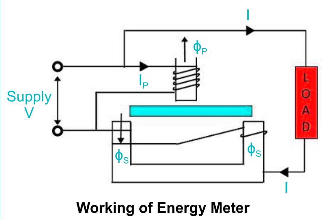
Construction of an Energy Meter
The construction of an energy meter can vary depending on the type (electromechanical, electronic, or smart). However, the general components include the following:
- Current Coil: This coil is placed in series with the load and carries the current to be measured. It generates a magnetic field that interacts with the magnetic field of the voltage coil, producing a mechanical torque in the case of electromechanical meters.
- Voltage Coil: The voltage coil produces a magnetic field that interacts with the one created by the current coil. The voltage coil generates a magnetic field that interacts with the magnetic field produced by the current coil.
- Rotating Disc (for electromechanical meters): The current and voltage coils generate a magnetic field that induces a torque on a metal disc. The disc rotates, and the speed of rotation is proportional to the power consumption. The mechanical motion of the disc drives the dials to display the energy used.
- Digital Display (for electronic meters): Instead of mechanical dials, electronic energy meters have a digital display that shows the energy consumption in numerical form. A microcontroller processes the data to update the display in real-time.
- Mechanical Dials: In older electromechanical meters, the disc’s motion is linked to a set of dials or gears that indicate the energy usage.
- Brake Mechanism: A friction brake mechanism is applied to slow down the rotation of the disc in electromechanical meters, ensuring the meter measures the energy consumption accurately.
- Transformer (optional): In some energy meters, especially for higher voltage systems, transformers are used to step down the voltage to safe, measurable levels.
Energy Meter Phasor Diagram
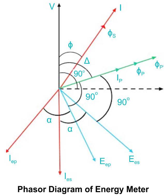
The phasor diagram is a graphical representation of the relationship between the voltage and current waveforms in an AC circuit. For energy meters, phasor diagrams help in understanding how the current and voltage are related, which is essential for accurate energy measurement.

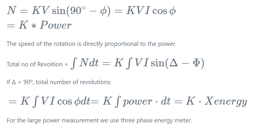
In a typical AC circuit, the voltage and current waveforms are sinusoidal but may be out of phase. The angle between the voltage and current phasors indicates the phase difference. For active power (real power), the voltage and current are in phase, and the power factor is unity (1). However, in most practical cases, the current and voltage are not perfectly in phase due to inductive or capacitive components, leading to a power factor less than 1.
The energy meter measures the product of voltage and current over time, which is then displayed as the energy consumption. The phase difference between the current and voltage is critical, as it influences the calculation of the true power (active power) that the energy meter records.
Conclusion
Energy meters are indispensable tools in modern electrical systems, providing accurate measurement and monitoring of electrical energy usage. Whether electromechanical, electronic, or smart meters, they all serve the primary function of measuring electrical consumption. Understanding the construction, working principles, and types of energy meters helps consumers and utilities optimize energy management and ensure efficient billing practices. Phasor diagrams are a useful tool in understanding the relationship between voltage and current, aiding in accurate energy measurement, particularly in AC circuits.
The post Energy Meter Definition, Types, Working, Construction & Diagram appeared first on ELE Times.
Analog IC vs Digital IC – Difference and Comparison
Integrated circuits (ICs) have revolutionized modern electronics, serving as the backbone of countless devices. Broadly, ICs are categorized into two main types: Analog ICs and Digital ICs. Understanding their differences and specific applications is essential for selecting the right components for various electronic systems. This article delves into the distinctions and comparisons between analog and digital ICs, highlighting their respective advantages, limitations, and use cases.
What are Analog ICs?
Analog ICs process continuous signals that vary over time and are used to manage real-world data such as sound, light, temperature, or pressure. These integrated circuits are crucial in scenarios that demand high precision and uncompromised signal quality.
Key Features of Analog ICs:
- Continuous Signal Processing: Operate with signals that have infinite values within a range.
- Signal Amplification and Conditioning: Amplify or modify analog signals for further processing.
- High Sensitivity: Analog ICs are ideal for handling small changes in signal amplitude.
Common Examples:
- Operational amplifiers (op-amps)
- Voltage regulators
- Analog-to-digital converters (ADCs)
- Audio amplifiers
What are Digital ICs?
Digital integrated circuits process discrete signals, encoding information in binary format, where data is represented as sequences of 0s and 1s. These ICs are integral to modern computing and communication systems.
Key Features of Digital ICs:
- Binary Signal Processing: Work with two distinct states, high (1) and low (0).
- Logical Operations: Perform arithmetic, logical, and control operations efficiently.
- Noise Immunity: Digital ICs demonstrate greater resilience to noise, making them more reliable in environments with high interference.
Common Examples:
- Microprocessors
- Memory chips (RAM, ROM)
- Logic gates
- Digital-to-analog converters (DACs)
Comparison Between Analog ICs and Digital ICs
| Aspect | Analog IC | Digital IC |
| Signal Type | Continuous signals | Discrete signals (binary) |
| Processing | Processes real-world, variable data | Processes binary data |
| Complexity | Simpler design | Higher complexity in circuits |
| Noise Sensitivity | More vulnerable to interference and distortions | More resistant to interference and noise disruptions |
| Applications | Audio, sensors, signal conditioning | Computing, storage, digital communication |
| Power Consumption | Generally higher for amplifiers | Lower for logic circuits |
| Accuracy | Depends on precision of components | High for binary operations |
| Speed | Limited by signal amplitude and frequency | Faster due to digital switching |
Hybrid ICs: Bridging the Gap
Modern systems often necessitate a combination of both analog and digital capabilities to function seamlessly. For instance, smartphones rely on analog ICs for signal acquisition (microphones, cameras) and digital ICs for processing (processors, memory). Hybrid ICs, which combine analog and digital components, are increasingly popular for such integrated applications.
Example:
- Analog-to-Digital Converters (ADCs) convert continuous analog inputs into a digital format, enabling their use in computational and processing systems.
- Digital-to-Analog Converters (DACs) take processed digital data and convert it back into analog signals for practical, real-world output.
Applications of Analog ICs
- Audio Equipment: Analog amplifiers and equalizers enhance sound quality in audio systems.
- Power Management: Voltage regulators and power amplifiers manage and stabilize power supplies.
- Sensors and Instrumentation: Analog ICs process data from temperature, pressure, and motion sensors.
Applications of Digital ICs
- Computing Devices: Microprocessors and memory chips drive computers and smartphones.
- Communication Systems: Digital signal processors (DSPs) enable data encoding, modulation, and transmission.
- Automation and Control: Logic circuits and microcontrollers power robotics and industrial automation.
Advantages and Disadvantages
Analog ICs:
- Advantages:
- Superior for real-world signal processing.
- Ideal for use in scenarios where maintaining high signal accuracy and integrity is essential.
- Disadvantages:
- More susceptible to interference and signal degradation.
- Larger power consumption for certain tasks.
Digital ICs:
- Advantages:
- High accuracy and noise immunity.
- Efficient for high-speed operations and complex computations.
- Disadvantages:
- Limited in handling real-world signals directly.
- Conversion to and from analog signals may introduce delays.
Conclusion
Analog and digital ICs serve distinct yet complementary roles in modern electronics. While analog ICs excel in processing real-world signals with precision, digital ICs dominate areas requiring speed, accuracy, and computational power. The synergy of these technologies, often realized in hybrid ICs, is driving innovation across industries such as healthcare, automotive, consumer electronics, and communication. Understanding the strengths and limitations of each type enables engineers and designers to create optimized and efficient electronic systems tailored to specific applications.
The post Analog IC vs Digital IC – Difference and Comparison appeared first on ELE Times.
Sparc the robot wiring
 | A homemade robot powered by arduino [link] [comments] |
NUBURU announces board and committee appointments
Voyant launches FMCW LiDAR sensor on a chip
DOE announces $179m funding for Microelectronics Science Research Centers
Exploring Space with Next-Gen Satellites and Electronics
The relentless pursuit of space exploration has always been a testament to humanity’s desire to push the boundaries of what’s possible. From the earliest satellite launches to interplanetary missions, the technological advances driving these achievements are nothing short of revolutionary. Among these, next-generation satellites and cutting-edge electronics are at the forefront, enabling unprecedented capabilities in communication, observation, and exploration.
The Evolution of Satellite Technology
The journey of satellite technology began in 1957 with the launch of Sputnik 1, a rudimentary metal sphere weighing just 83.6 kilograms. Since then, satellites have evolved from basic communication devices to complex systems that underpin modern society. Today’s satellites are miniature marvels, integrating advanced materials, AI-driven systems, and versatile designs to meet a myriad of demands.
- Miniaturization and Cost Reduction: With advancements in microelectronics and manufacturing techniques, the size and cost of satellites have drastically decreased. CubeSats and nanosatellites, often no larger than a shoebox, are increasingly common, democratizing space access for academic institutions, startups, and developing nations.
- Increased Functionality: Modern satellites boast multi-functional capabilities, combining Earth observation, weather monitoring, and communication tasks in a single platform.
- Enhanced Durability: New materials and radiation-resistant electronics extend satellite lifespans, reducing the frequency and cost of replacements.
Cutting-Edge Electronics in Space Exploration
The electronics onboard spacecraft are critical to their success, operating in extreme conditions of temperature, radiation, and vacuum. Next-generation electronic systems are pushing the boundaries of what’s feasible in these harsh environments.
- Radiation-Hardened Components: Space electronics are designed to withstand intense radiation and high-energy particles. Innovations in semiconductor manufacturing, such as gallium nitride (GaN) and silicon carbide (SiC) technologies, enhance performance while ensuring reliability.
- AI and Edge Computing: Artificial Intelligence (AI) empowers satellites to operate independently by analyzing data and making decisions on the fly, significantly reducing dependency on ground control
- Energy Efficiency: Power consumption is a critical factor in space. Advances in low-power processors and energy-harvesting technologies, like solar arrays and thermal converters, ensure sustainable operations.
Transformative Applications of Next-Gen Satellites
The advancements in satellite technology and electronics have unlocked transformative applications across industries and domains. Here are some key domains impacted:
- Global Connectivity: Initiatives like SpaceX’s Starlink and OneWeb aim to provide high-speed internet access to even the most remote areas, bridging the digital divide and fostering economic growth.
- Earth Observation: Satellites equipped with high-resolution cameras and advanced sensors are pivotal for environmental monitoring, disaster response, and agricultural optimization.
- Space-Based Navigation: Next-gen satellites improve the accuracy and reliability of Global Navigation Satellite Systems (GNSS), enhancing applications from autonomous vehicles to precision farming.
- Deep Space Missions: Advanced electronics enable missions to Mars, asteroids, and beyond, with improved data transmission rates, robust hardware, and autonomous systems to handle the challenges of interplanetary travel.
Latest Case Studies
Recent case studies highlight the real-world impact of next-gen satellites and electronics. For instance, the European Space Agency’s (ESA) Copernicus Sentinel program uses cutting-edge satellites to monitor climate change, providing invaluable data for policymakers worldwide. Similarly, NASA’s Perseverance rover, equipped with advanced electronic systems, has been exploring Mars, collecting samples, and sending high-definition images back to Earth. Another example is SpaceX’s Starlink constellation, which has successfully deployed over 5,000 satellites, revolutionizing global broadband connectivity and demonstrating the scalability of modern satellite networks.
Challenges and Innovations
Despite these advancements, the journey toward next-gen satellites and electronics is not without challenges. Addressing these hurdles requires innovative solutions and collaborative efforts.
- Thermal Management: Extreme temperatures in space necessitate effective thermal management systems. Novel materials and phase-change technologies are being developed to dissipate heat efficiently.
- Space Debris Mitigation: The proliferation of satellites increases the risk of collisions and debris generation. Technologies like satellite-servicing robots, deorbiting mechanisms, and enhanced tracking systems are crucial for sustainable space operations.
- Data Security: As satellites become integral to global infrastructure, they face growing cybersecurity threats. Implementing quantum encryption and blockchain technology can enhance security.
- Supply Chain Constraints: The demand for specialized components, coupled with geopolitical factors, poses challenges to satellite production. Investments in domestic manufacturing and diversified sourcing are essential.
The Role of AI and Machine Learning
AI and Machine Learning (ML) are revolutionizing how satellites operate and interact with their environments. From autonomous navigation to predictive maintenance, these technologies are key enablers of next-gen satellite capabilities.
- Autonomous Navigation: AI algorithms allow satellites to adjust their orbits and avoid collisions autonomously, ensuring operational continuity.
- Predictive Maintenance: ML models analyze telemetry data to predict and prevent system failures, extending satellite lifespans.
- Dynamic Tasking: AI enables satellites to prioritize tasks based on real-time data, optimizing resource utilization.
Collaboration and the Future
The development of next-generation satellites and electronics is a global endeavor, with governments, private companies, and academic institutions contributing to the effort. Collaborative initiatives like NASA’s Artemis program, ESA’s Earth Observation missions, and ISRO’s Chandrayaan projects exemplify the collective drive to explore space.
The private sector also plays a pivotal role. Companies like SpaceX, Blue Origin, and Rocket Lab are not only advancing satellite technology but also redefining space transportation and logistics. Meanwhile, electronics giants are investing heavily in research and development to create components tailored for space applications.
Conclusion
Next-generation satellites and electronics are the backbone of modern space exploration and utilization. They enable groundbreaking applications, from global connectivity to interplanetary missions, while addressing challenges with innovative solutions. As humanity continues to explore the cosmos, the synergy between satellite technology and advanced electronics will undoubtedly shape the future of space exploration and its benefits for life on Earth.
The post Exploring Space with Next-Gen Satellites and Electronics appeared first on ELE Times.
Human Augmentation Tech: Bridging Electronics and Biology
In recent years, human augmentation technology has transitioned from science fiction to an exciting frontier of innovation. Bridging the gap between electronics and biology, this emerging field holds the promise to enhance human capabilities, address disabilities, and redefine our relationship with technology. By integrating advanced electronics into the human body, researchers and engineers are unlocking unprecedented possibilities in healthcare, communication, and even daily life.
Understanding Human AugmentationHuman augmentation refers to the application of technology to enhance or restore physical, cognitive, and sensory abilities. These enhancements can be divided into three broad categories:
- Physical Augmentation: Technologies that enhance physical strength, mobility, or endurance. Examples include exoskeletons and prosthetics.
- Cognitive Augmentation: Tools that boost mental capabilities such as memory, problem-solving, and learning.
- Sensory Augmentation: Devices that enhance or restore sensory perception, such as hearing aids, cochlear implants, or visual prostheses.
- Prosthetics and Bionics
Advanced prosthetics and bionic devices are redefining what it means to live with a disability. Prosthetic limbs equipped with sensors and actuators can replicate natural movements, while neural interfaces enable users to control these devices using brain signals. For instance, DARPA’s Brain-Machine Interface (BMI) program has developed prosthetics capable of providing tactile feedback, offering users a sense of touch.
- Exoskeletons
Exoskeletons are wearable devices that augment strength and mobility. Used in industries such as healthcare, military, and manufacturing, these devices reduce physical strain and assist individuals with mobility impairments. Companies like Ekso Bionics and ReWalk Robotics are leading the way in commercializing exoskeleton technologies.
- Brain-Computer Interfaces (BCIs)
BCIs establish direct communication between the brain and external devices. This technology is instrumental in restoring communication for individuals with severe paralysis. Neuralink, a company founded by Elon Musk, is pioneering BCIs that aim to treat neurological conditions and enable direct interaction with digital devices.
- Sensory Augmentation Devices
Sensory augmentation focuses on restoring or enhancing sensory inputs. Cochlear implants, for example, have revolutionized hearing restoration, while retinal implants like the Argus II are helping individuals with certain types of blindness regain partial vision. Innovations in haptic feedback systems are also enabling users to experience touch in virtual and augmented reality environments.
- Gene Editing and Bioengineering
Gene-editing technologies like CRISPR-Cas9 are paving the way for biological augmentation. By altering genetic codes, scientists aim to enhance immunity, improve cognitive functions, and even extend lifespan. Although still in its infancy, this area holds tremendous potential for preventive healthcare and personalized medicine.
Applications of Human AugmentationHealthcare
Human augmentation is already transforming the healthcare sector. From robotic surgical systems that enhance precision to wearable devices monitoring real-time health metrics, technology is enabling proactive and personalized medical care. For individuals with disabilities, augmentation devices are restoring independence and improving quality of life.
Military and Defense
Exoskeletons and augmented reality systems are being developed to enhance soldier capabilities on the battlefield. Augmented soldiers equipped with heads-up displays and enhanced communication systems can process critical information faster, improving decision-making in high-stress environments.
Workplace Productivity
In industrial settings, exoskeletons reduce fatigue and injury among workers by assisting with heavy lifting and repetitive tasks. Cognitive augmentation tools, such as AI-driven analytics platforms, are enhancing decision-making and problem-solving in office environments.
Education and Learning
Augmented reality (AR) and virtual reality (VR) technologies are creating immersive learning experiences. Cognitive augmentation tools are also helping students with learning disabilities by providing tailored educational content and improving focus.
Entertainment and Gaming
Wearable devices and haptic feedback systems are enhancing the gaming experience, allowing players to interact with virtual environments in unprecedented ways. Sensory augmentation devices are also enabling more inclusive gaming for individuals with disabilities.
Challenges in Human AugmentationWhile the potential of human augmentation is immense, the field faces several challenges:
Ethical Concerns
The integration of technology with human biology raises profound ethical questions. Should augmented individuals be given competitive advantages in education or the workplace? How do we ensure equitable access to these technologies?
Privacy and Security
Devices like BCIs and wearable health monitors collect sensitive data, making them potential targets for cyberattacks. Establishing robust security protocols and data privacy standards is essential to address these concerns.
Biocompatibility and Safety
Ensuring that augmentation devices are safe and compatible with the human body is critical. Long-term studies are necessary to assess the potential risks and side effects of implantable technologies.
Cost and Accessibility
Many human augmentation technologies are expensive, limiting their accessibility. Scaling production and developing cost-effective solutions will be vital to democratizing these innovations.
Future Directions in Human AugmentationAdvancements in AI and Machine Learning
AI is playing a pivotal role in enhancing human augmentation technologies. Machine learning algorithms are improving the functionality of prosthetics, enabling them to adapt to user behavior. AI-driven insights are also optimizing BCI systems and making real-time health monitoring more accurate.
Development of Soft Robotics
Soft robotics, which uses flexible materials, is revolutionizing wearable devices and prosthetics. These systems are more comfortable and better mimic natural movements, providing a seamless user experience.
Integration with 5G and IoT
The deployment of 5G networks and the Internet of Things (IoT) is facilitating seamless communication between augmentation devices and external systems. Real-time data exchange will enable faster decision-making and improved device functionality.
Focus on Sustainable Materials
To address environmental concerns, researchers are exploring sustainable and biodegradable materials for augmentation devices. These materials not only reduce ecological impact but also enhance biocompatibility.
Global Collaboration
Collaboration between governments, private sectors, and academic institutions is accelerating innovation in human augmentation. International partnerships are driving research, standardizing regulations, and ensuring ethical practices.
The Social Impact of Human AugmentationHuman augmentation has the potential to redefine societal norms. By addressing disabilities and enhancing abilities, these technologies can foster inclusivity and equity. However, they also risk widening social inequalities if access is limited to privileged groups. Balancing innovation with accessibility and ethical considerations will be crucial for harnessing the full potential of human augmentation.
ConclusionHuman augmentation technology represents a remarkable fusion of electronics and biology, pushing the boundaries of what humans can achieve. While challenges remain, ongoing advancements in AI, robotics, and biotechnology are paving the way for a future where augmented capabilities are an integral part of daily life. As we navigate this transformative era, fostering a collaborative, ethical, and inclusive approach will be key to ensuring these innovations benefit humanity as a whole.
The post Human Augmentation Tech: Bridging Electronics and Biology appeared first on ELE Times.
Pages

