
Feed aggregator
Infineon AIROC CYW20829 to support Engineered for Intel Evo Laptop Accessories Program
Infineon Technologies AG announced that its AIROC CYW20829 Bluetooth LE microcontroller (MCU) and Software Development kit (SDK) are now verified as part of the Engineered for Intel Evo laptop accessory program, the first of its kind in the Bluetooth human interface device (HID) industry. Through this collaboration with Intel, vendors developing next generation HID devices can confidently “ditch the dongle” using CYW20829. With this new solution, designers can achieve a best-in-class direct-to-host connection which has been rigorously tested against Intel’s strict KPIs and experience requirements.
“At Infineon, we strive to provide a leading wireless experience and convenience to consumers and designers,” said Shantanu Bhalerao, Vice President of Wireless Products at Infineon Technologies. “With over two decades of wireless HID experience, we are delighted to support the Engineered for Intel Evo program with our CYW20829, optimizing the user experience for both vendors and customers by helping them to truly eliminate the dongle.”
The Intel Evo platform is Intel’s superior consumer brand for premium laptops. Designed to provide a premium computing experience, laptop designs that meet the Intel Evo requirements undergo rigorous testing measurement and verification to ensure they deliver exemplary performance in terms of responsiveness, battery life, charging capability, form factor, and more. Engineered for Intel Evo Laptop Accessories Program defines strict Intel requirements for Bluetooth PC Peripherals, maximizing the end-to-end user experience when paired with Intel Evo laptops.
“Wireless peripherals are essential ingredients for the execution of many of our day-to-day computing activities,” said Eric McLaughlin, VP & GM, Connectivity Solutions Group at Intel Corporation. “For this reason, Intel works closely with key partners to ensure their devices meet technical requirements in the areas of performance, reliability, and ease of use. We’re excited that the Engineered for Intel Evo accessory program is expanding to include Infineon’s AIROC CYW20829 Bluetooth LE MCU and SDK, further extending Intel’s industry collaboration towards the goal of enabling amazing end-to-end connected user experiences.”
Infineon’s CYW20829 Bluetooth LE microcontroller (MCU) was designed with HID applications in mind to include:
- RF Performance: Featuring a dual demodulator architecture, long-standing Rx Blocker IP, and link budget of 108 dB, CYW20829 delivers unprecedented wireless robustness.
- Power Optimization: CYW20829 delivers up to 20 percent better battery life over leading devices in the market through its ARM Cortex-M33 clocking at 48 or 96 MHz, hardware keyscan matrix to buffer user inputs without core activation, and superb Tx & Rx current consumption.
- Cost: Highly integrated and unburdened with unnecessary peripherals, the CYW20829 is cost competitive with low-cost package offerings and the ability to route on 2-layer non-HDI PCB.
- Security: CYW20829 features support for the emerging Cyber Resiliency Act (CRA) and Radio Equipment Directive (RED) security regulations which will be mandatory for wireless products being sold on the European market.
- Zephyr: Enabled and supported on CYW20829, Zephyr addresses the growing number of OEMs leveraging the operating system.
The post Infineon AIROC CYW20829 to support Engineered for Intel Evo Laptop Accessories Program appeared first on ELE Times.
The Best Substation Training Programs
The best substation training program gives energy professionals the tools and knowledge to navigate the complexity of modern power systems. This sector involves advanced technology and evolving regulations that demand precision and adaptability. These programs focus on the real-world skills to keep operations safe, reliable and compliant with industry standards.
Substations serve as critical hubs in the power grid, and even small errors can lead to costly downtime or serious safety risks. This makes specialized training a must for technicians and engineers. Combining technical expertise with a deep understanding of safety protocols prepares professionals to work confidently with high-voltage equipment, adapt to new digital systems and meet the regulatory demands of the energy sector.
- TRC Power Academy
TRC Power Academy is a top-tier training provider for substation professionals, thanks to its industry-aligned, hands-on approach that mirrors real utility environments. It has a cutting-edge training center in Lancaster, Pennsylvania, with a full-scale mock substation, complete with control house, yard, circuit-breaker and transformer simulators. Its facilities let engineers and technicians learn in a safe yet realistic setting.
Backed by experienced utility engineers, its courses cover relay protection, substation drawings, power transformers and outage planning. These programs are delivered through instructor-led sessions and self-paced online modules that meet the International Electrical Testing Association (NETA) standards.
Beyond fundamentals, TRC Power Academy includes a 10-week training sequence followed by six months of field application and advanced refresher sessions. This rare opportunity fosters real professional connections while reinforcing safety and technical consistency. For energy and inspection professionals who want deep learning in a practical, engaging environment, TRC Power Academy delivers with clarity, credibility and career-building momentum.
- Siemens Power Academy
Siemens Power Academy offers users a highly interactive and expert training experience tailored to energy professionals. It offers more than 300 curated courses — including core substation automation, protection, digital substations and cybersecurity — through hands-on workshops, virtual sessions and simulation-based options.
Its structured course catalog spans crucial topics, such as substation automation, distributed energy automation, self-consistent-charge parameterization and Process Bus integration. It covers station- and process-level digital substation design and cutting-edge modules on microgrids, grid planning and smart communication systems.
Participants benefit from training personalization through Siemens’ consultative approach, which ensures each learner’s unique goals align with their curriculum. They can enjoy flexible delivery formats — classroom, on-site, e‑learning or simulator‑based — to fit different learning styles and schedules. For professionals in energy and inspection services seeking advanced, credible and future-ready training, Siemens offers the depth in substation technology and delivery flexibility to stay ahead in the field.
- GE Digital Energy Training Programs
The GE Digital Energy Training Program is an exceptional partner for substation training because it offers a comprehensive and flexible learning ecosystem that blends technical depth with real-world relevance. Its global network of technical institutes delivers hands‑on courses in electrical grid safety, equipment operations, protection, control and network management. These programs are taught by seasoned experts using full‑size gas-insulated bays, air-insulated substation components and real equipment to bridge theory with practice.
Participants can undergo modern training formats, including virtual reality modules that simulate real-world procedures, modular classroom instruction and customizable certification tracks. Courses cover various topics such as gas-insulated substation fundamentals, digital substation systems and high‑voltage substation environments. These modules deliver practical skills and theoretical understanding in formats tailored to engineers and new professionals.
The GE Digital Energy Training Programs come with assessments and certification, which ensure learning matches individual needs and modern delivery preferences. It equips energy and inspection professionals with cutting-edge, adaptable training that builds competence and career momentum.
- ABB Power Grids Learning Center
ABB Power Grids Learning Center provides a robust training ecosystem through its ABB University. It offers targeted programs on digital substation products and modern protection systems. These programs offer flexible delivery — interactive classroom sessions, e-learning, webinars and fully tailored on-site courses — so learners can engage in the format that best fits their goals.
Trainees gain hands-on access to protection and control relays with the guidance of expert trainers. They can master everything, such as basic relay operations, advanced engineering, application specifics and critical topics like cybersecurity and fault management. ABB’s commitment to customization ensures its training comes in multiple languages and is delivered securely via VPN when necessary.
ABB offers up-to-date course content, global accessibility, a practical focus and a strong emphasis on safe, reliable system operation. With its legacy of innovation behind it, its training stands out as a compelling choice for professionals aiming to boost their substation expertise and operational confidence.
- Eaton Electrical Engineering Services & Training
Eaton Electrical Engineering Services & Training delivers exceptional substation and electrical training. Its experience centers give energy professionals a versatile, high-impact learning path in real-world environments. With over a century of expertise in power systems and decades of hands-on experience, Eaton combines deep industry knowledge with flexible course formats.
It offers in‑person instruction at world-class facilities in Pittsburgh and Houston, remote instruction, eLearning and even virtual simulations. Learners can train anywhere on topics like power distribution equipment, testing, safety, relay and transformer maintenance, compliance, and arc flash protection. Its instructors are seasoned field engineers who actively shape industry safety standards, which ensures training stays current and authoritative.
Eaton’s hands-on offerings include courses like Basic Protective Relay Testing, Transformer Startup and Maintenance, Power Quality Monitoring and Analysis, and Electrical and Arc Flash Safety. It blends practical insight, recognized credentials and schedule-friendly delivery, making it a smart, credible choice for substation-focused learning in the energy and inspection sector.
- Megger Training Services
Megger Training Services equips technicians and apprentices with hands‑on skills and solid technical know‑how. Its Substation Maintenance I course guides participants in safely maintaining and testing industrial and utility substation equipment. It includes immersive lab sessions focused on medium-voltage circuit breakers and switchgear, which help learners spot weak components and ensure operational readiness.
For those ready to level up, Substation Maintenance II provides advanced training centered on transformer-related operations, expanding on the foundational skills from the first course. These courses feed into a robust Substation Technician Certification program that validates mastery in maintaining breakers, transformers, safety protocols and relevant OSHA standards.
Beyond classroom training, Megger enhances ongoing skill development via expert-led webinars and a rich online knowledge hub with technical articles and support. Megger combines practical, high-impact classroom experiences with accessible learning tools and recognized credentials. It gives energy professionals the tools, confidence and recognition they need to excel in substation operations.
- Schweitzer Engineering Laboratories (SEL) University
Schweitzer Engineering Laboratories (SEL) University delivers a standout substation training experience. It equips engineers and managers with a full spectrum of learning options, including in-person, virtual and self-paced e-learning formats to suit every schedule and learning preference.
Its programs span a range of specialized courses. The Transmission Substation Relay Testing class teaches learners to input settings, test, commission and troubleshoot relays via immersive exercises. Meanwhile, Substation Equipment Protection dives deep into protection schemes for high-voltage transformers, buses, capacitor banks and reactors. It includes real-world fault analysis and relay setting calculations.
Beyond course delivery, SEL diligently instills real-world safety. Its Charlotte facility features a simulator of a substation control house and yard where staff train on hazard avoidance in realistic scenarios. SEL University offers unmatched expertise, credibility and adaptability in substation education. It’s ideal for energy and inspection professionals seeking deep, practical and grounded in real control environments.
- American Public Power Association (APPA) Academy
The American Public Power Association (APPA) Academy supports public power utilities with tailored workforce development. It offers in‑person seminars, certificate programs, webinars and on-demand training that often include critical substation safety and maintenance content in its utility-focused courses.
For example, Snohomish County Public Utilities District hosted a five‑day course blending electrical theory and hands‑on training. It taught technicians how to test equipment and identify trends that signal imminent failure, which reinforces reliability and safety in substation operations. Working with APPA, the Missouri Public Utility Alliance also launched a two‑week apprenticeship that includes substation safety training. It helped apprentices gain real‑world substation skills alongside foundational distribution practices.
Alongside supportive resources like the APPA Safety Manual, these offerings make APPA a valuable ally for utilities aiming to elevate substation training, maintain compliance and reinforce safety. Engaging with APPA and its network means tapping into community-curated tools, collaborative training opportunities and up-to-date safety frameworks that help energy and inspection professionals.
- Electric Power Research Institute (EPRI) Training Programs
The Electric Power Research Institute (EPRI) Training Programs offer impressive, on-demand webinars and workshops tailored to substation topics. These include dissolved gas analysis, partial discharge detection, transformer monitoring and circuit-breaker restrike explanations. Each program delivers deep technical insight in a flexible, self-paced format.
These training modules blend research-backed content with real-world application. They are ideal for energy and inspection professionals seeking to sharpen their expertise on transformer condition monitoring, substation equipment behavior or fault detection methods. Further, EPRI offers instructor-led workshops like the Substation Ground Grid Inspection Workshop, delivering hands-on inspection techniques and peer-to-peer learning that bring theory to life.
As a nonprofit research authority, EPRI delivers up-to-date best practices rooted in industry science and innovation. It’s a smart, credible choice for professionals who value evidence-based learning and want to stay ahead in substation operations and reliability.
Skills and Competencies Gained From Substation TrainingThe best substation training program gives energy professionals the well-rounded expertise to excel in the power industry. It builds technical competencies by teaching precise equipment operation, thorough switchgear maintenance and the intricate workings of relay protection systems.
Safety and compliance are woven into every lesson, with practical instruction in electrical hazard awareness, lockout/tagout procedures and arc flash protection that keeps people and infrastructure secure. Learners also develop sharp inspection and testing skills, using diagnostic tools, thermography and proper gas handling to spot issues before they escalate.
To future-proof their careers, participants gain insight into emerging technologies like digital substations, smart monitoring systems and remote diagnostics. These skills align with the industry’s shift toward smarter, more connected grids. By blending hands-on practice with forward-looking knowledge, the best programs ensure professionals can work confidently, meet compliance demands and adapt to whatever the grid’s future holds.
Maximizing Career Impact From the Best Substation Training ProgramCertifications from reputable training programs are powerful career accelerators in the energy sector. They signal to employers and clients that a professional meets recognized industry standards and has the skills to handle complex, high-stakes work. They often open doors to higher-level positions, specialized project assignments and increased earning potential.
Many training providers also foster valuable networking opportunities, which connect participants with peers, industry veterans and potential employers through workshops and alumni networks. These connections can lead to collaborations, mentorships and job referrals that would be hard to find otherwise.
Ongoing certification also helps professionals stay ahead of compliance and safety requirements. It ensures their work practices align with evolving regulations, technical standards and industry best practices, keeping careers and operations future-ready.
Industry Trends Shaping Substation TrainingThe best substation training program prepares professionals to thrive in a sector reshaped by digitalization and automation, and they use smart systems to streamline operations and boost efficiency. Participants learn to work with AI-driven monitoring tools that enhance predictive maintenance, detect faults in real time and improve grid reliability.
With renewables integration and energy storage transforming how substations balance supply and demand, the program equips learners with the skills to manage these new complexities while maintaining stability and compliance. It also embraces the post-pandemic shift toward remote training technologies, offering interactive virtual simulations and online modules that make advanced learning accessible without sacrificing hands-on experience.
How to Choose the Best Substation Training ProgramChoosing the right substation training program can significantly impact your career growth, technical skills and safety expertise. With so many options available, evaluating each program based on your professional goals, industry requirements and preferred learning style is important. The best choice will deepen your technical knowledge and provide recognized credentials and practical experience that translate directly to your work in the field.
- Check industry recognition and accreditation: Ensure the program is backed by reputable organizations and aligns with standards from bodies like NETA or OSHA.
- Look for experienced instructors: Choose providers whose trainers have real-world substation and utility experience.
- Evaluate hands-on training opportunities: Prioritize programs that offer lab work, equipment simulations or on-site practice to apply concepts in realistic scenarios.
- Confirm coverage of compliance and safety: Make sure the curriculum includes current safety protocols and hazard mitigation strategies.
- Review available learning formats: Select a delivery method that fits your schedule and learning style.
- Assess technology and facilities: For in-person training, look for modern equipment and simulation setups that mirror real substation environments.
- Consider post-training support: See if the provider offers refresher courses, alum networks or ongoing technical resources.
- Match the program to your career stage: Beginners may need foundational courses, while seasoned professionals might benefit more from advanced or specialized modules.
Continuous learning in substation operations ensures professionals stay ahead of technologies, safety standards and regulatory requirements. You gain skills that strengthen performance and career growth by choosing the best substation training program. Evaluate programs based on current industry demands and the competencies you will need for the future.
The post The Best Substation Training Programs appeared first on ELE Times.
European Project to Repurpose Fiber-Optic Cables Into Photonic Sensors
IR Obstruction Detector
 | Nice day-off project. I know it's pretty dated style, but I just really love using nothing more than a pin-out diagram for the components, and going from there. I start by placing the button and a regulator, and then the smoothing capacitors, then the power LED and its power limiting resistor. This was made on stripboard, so each column is common, except for where I cut the traces under the 555 socket, to prevent pins 1-8, 2-7, etc from being shorted together. [link] [comments] |
I don't think that any part of the circuitry in a metro station elevatr should look like this
 | submitted by /u/Elvenblood7E7 [link] [comments] |
Toshiba Improves MOSFET Performance With Advanced Packaging
Just cleaned about 5 square meters of vintage mixer PCBs.
 | Mmm capacitor juice and grime. Series Ten Mixer btw :3 [link] [comments] |
Increasing bit resolution with oversampling
 Increasing ADC resolution
Many electronic designs contain an ADC, or more than one, to read various signals and voltages. Often, these ADCs are included as part of the microcontroller (MCU) being used. This means, once you pick your MCU, you have chosen the maximum resolution (calculated from the number of bits in the ADC and the reference) you will have for taking a reading.
Wow the engineering world with your unique design: Design Ideas Submission Guide
What happens if, later in the design, you find out you need slightly more resolution from the ADC? Not to worry, there are some simple ways to improve the resolution of the sampled data. I discussed one method in a previous EDN Design Idea (DI), “Adaptive resolution for ADCs,” which talked about changing the reference voltage, so I won’t discuss that here. Another way of improving the resolution is through the concept of oversampling.
Let’s first look at a method that is essentially a simplified version of oversampling…averaging. (Most embedded programmers have used averaging to improve their readings, sometimes with the thought of minimizing the effects of bad readings and not thinking about improving resolution.)
So, suppose you’re taking a temperature reading from a sensor once a second. Now, to get a better resolution of the temperature, take the reading every 500 ms and average the two readings together. This will give you another ½-bit of resolution (we’ll show the math later). Let’s go further—take readings every 250 ms and average four readings. This will give you a whole extra bit of resolution.
If you have an 8-bit ADC and it is scaled to read 0 to 255 degrees with 1-degree resolution, you will now have a virtual 9-bit ADC capable of returning readings of 0 to 255.5 degrees with 0.5-degree resolution. If you average 16 readings, you will create a virtual 10-bit ADC from your 8-bit ADC. The 64-averaged reading will create an 11-bit virtual ADC by improving your 8-bit ADC with three extra bits, thereby giving you a resolution of one part in 2048 (or, in the temperature sensor example, a resolution of about 0.12 degrees).
A formula for averagingThe formula for extra bits versus the number of samples averaged is:
Number of samples averaged = M
Number of virtual bits created = b
M = 4b
If you want to solve for b given M: b = log4(M)
Or, b = (1/ log2(4)) * log2(M) = log2(M)/2
You may be scratching your head, wondering where that formula comes from. First, let’s think about the readings we are averaging. They consist of two parts. The first is the true, clean reading the sensor is trying to give us. The second part is the noise that we pick up from extraneous signals on the wiring, power supplies, components, etc. (These two signal parts combine in an additive way.)
We will assume that this noise is Gaussian (statistically normally distributed; often shown as a bell curve; sometimes referred to as white noise) and uncorrelated to our sample rate. Now, when taking the average, we first sum up the readings. The clean readings from the sensor will obviously sum up in a typical mathematical way. In the noise part, though, the standard deviation of the sum is the square root of the sum of the standard deviations. In other words, the clean part increases linearly, and the noise part increases as the square root of the number of readings.
What this means is that not only is the resolution increased, but the signal-to-noise ratio (SNR) would improve by M/sqrt(M), which mathematically reduces to sqrt(M). In simpler terms, the averaged reading SNR improves by the square root of the number of samples averaged. So, if we take four readings, the average SNR improves by 2, or the equivalent of one more bit in the ADC (an 8-bit ADC performs as a 9-bit ADC).
I have used averaging in many pieces of firmware, but it’s not always the best solution. As was said before, your sensor connection is passing your ADC a good signal with some noise added to it. Simple averaging is not always the best solution. One issue is the slow roll-off in the frequency domain. Also, the stopband attenuation is not very good. Both of these issues indicate that averaging allows a good portion of the noise to enter your signal. So, we may have increased the resolution of the reading, but have not removed all the noise from the signal we can.
Reducing the noiseTo reduce this noise, that is spread over the full frequency spectrum coming down the sensor wire, you may want to apply an actual lowpass filter (LPF) to the signal. This can be done as a hardware LPF applied before the ADC or it can be a digital LPF applied after the ADC, or it can be both. (Oversampling makes the design of these filters easier as the roll-off can be less steep.)
There are many types of digital filters but the two major ones are the finite impulse response (FIR) and the infinite impulse response (IIR). I won’t go into the details of these filters here, but just say that these can be designed using tradeoffs of bandpass frequency, roll-off rate, ripple, phase shift, etc.
A more advanced approach to oversamplingSo, let’s look at a design to create a more advanced oversampling system. Figure 1 shows a typical layout for a more “formal”, and better oversampling design.

Figure 1 A typical oversampling block diagram with an antialiasing filter, ADC, digital LPF, and decimation (down-sampling).
We start by filtering the incoming signal with an analog hardware LPF (often referred to as an antialiasing filter). This filter is typically designed to filter the incoming desired signal at just above the frequency of interest.
The ADC then samples the signal at a rate many times (M) the frequency of interest’s Nyquist rate. Then, in the system’s firmware, the incoming sample stream is again low-pass filtered with a digital filter (typically an FIR or IIR) to further remove the signal’s Gaussian noise as well as the quantization noise created during the ADC operation. (Various filter designs can also be useful for other kinds of noise, such as impulse noise, burst noise, etc.) Oversampling gave us the benefit of spreading the noise over the wide oversample bandwidth, and our digital lowpass filter can remove much of this.
Next, we decimate the signal’s data stream. Decimation (also known as down-sampling) is simply the act of now only using every 2nd, or 3rd, or 4th, up to every Mth sample, and tossing the rest. This is safe due to oversampling and the lowpass filters, so we won’t alias much noise into the lower sample rate signal. Decimation essentially reduces the bandwidth as represented by the remaining samples. Further processing now requires less processing power as the number of samples is significantly reduced.
It worksThis stuff really works. I once worked on a design that required us to receive very small signals being transmitted on a power line (< 1 W). The signal was attenuated by capacitors on the lines, various transformers, and all the customer’s devices plugged into the powerline. The signal to be received was around 10 µV riding on the 240-VAC line. We ended up oversampling by around 75 million times the Nyquist rate and were able to successfully receive the transmissions at over 100 miles from the transmitter.
Damian Bonicatto is a consulting engineer with decades of experience in embedded hardware, firmware, and system design. He holds over 30 patents.
Phoenix Bonicatto is a freelance writer.
Related Content
- Adaptive resolution for ADCs
- Understanding noise, ENOB, and effective resolution in ADCs
- How do ADCs work?
- Understand key ADC specs
The post Increasing bit resolution with oversampling appeared first on EDN.
Deep Learning Architecture Definition, Types and Diagram
Deep learning architecture pertains to the design and arrangement of neural networks, enabling machines to learn from data and make intelligent decisions. Inspired by the structure of the human brain, these architectures comprise many layers of nodes connected to one another to gain increasing abstraction. As data goes through these layers, the network learns to recognize patterns, extract features, and perform tasks such as classification, prediction, or generation. Deep learning architectures have brought about a paradigm shift in the fields of image recognition, natural language processing, and autonomous systems, empowering computers with a degree of precision and adaptability to interpret inputs brought forth by human intelligence.
Deep Learning Architecture Diagram:
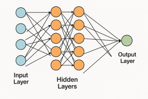
Diagram Explanation:
This illustration describes a feedforward network, a simple deep learning model wherein data travels from input to output in one direction only. It begins with an input layer, where, for example, every node would be a feature, fully connecting with nodes in the next hidden layer. The hidden layers (two layers of five nodes each) now transform the data with weights and activation functions, while every node in one layer connects with every node in the other layer: this complexity aids the network in learning complicated patterns. The output layer produces the final prediction-fully connected with the last hidden layer, it uses sigmoid in case of binary classification or softmax in case of multi-class. The arrows represent weights, which get adjusted during training to minimize the cost function.
Types of Deep Learning Architecture:
- Feedforward Neural Networks (FNNs)
The simplest cases of neural networks used for classification and regression with a unidirectional flow of data from input to output form the basis for more complicated architectures
- Convolutional Neural Networks (CNNs)
CNNs process image data by applying convolutional layers to detect spatial features. They are widely used in image classification, object detection, and medical image analysis because they can capture local patterns.
- Recurrent Neural Networks (RNNs)
RNNs are ideal for working with sequential data such as time series or text data. The loops hold in memory information or state of previous computations, which prove useful in speech recognition and language modeling.
- Long Short-Term Memory Networks (LSTMs)
LSTMs, which in turn are a type of RNN, can learn long-term dependencies as they utilize gates to control the flow of information through the cell. Some of their main uses include machine translation, music generation, and text prediction.
- Variational Autoencoders (VAEs)
With the addition of probabilistic elements, a VAE extends the traditional autoencoder and can, therefore, generate new data samples. They find their use in generative modeling of images and text.
- Generative Adversarial Networks (GANs)
GANs work by pitting two networks, a generator and a discriminator, against each other to create realistic data. They are known for producing high-quality images, deepfakes, and art.
- Transformers
Transformers use self-attention to study sequences in parallel, making them excellent models in natural language processing. Models like BERT, GPT, and T5 use the Transformer as their backbone.
- Graph Neural Networks (GNNs)
GNNs operate on graph-structured data; for example: social networks, or molecular structures. They learn representations by aggregating information from neighboring nodes-and are powerful for relational reasoning.
- Autoencoders
These are unsupervised models that learn to compress and then reconstruct data. Autoencoders are also used for dimensionality reduction, anomaly detection, and image denoising.
- Deep Belief Networks (DBNs)
DBNs are networks with multiple layers of restricted Boltzmann machines. They are used for unsupervised feature learning and pretraining of deep networks, which are then fine-tuned with supervised learning.
Conclusion:
Deep learning architectures are the backbone of modern AI systems. Each type, be it a simple feedforward network or an advanced transformer, possesses unique strengths suited to particular applications. With the continuing evolution of deep learning, hybrid architectures and efficient models are poised to spark breakthroughs in healthcare, autonomous systems, and generative AI.
The post Deep Learning Architecture Definition, Types and Diagram appeared first on ELE Times.
CCFL inverter from an old monitor
 | The scree got water damage, but this still works, the tubes will light up. Also, these transformers look quite similar to the ones found in CRTs. I wonder... [link] [comments] |
How JSD Electronics Uses AI and Machine Vision to Deliver Zero-Defect Electronics
In an exclusive interview with ELE Times, Mr. Deep Hans Aroraa, Co-Founder & Director at JSD Electronics, discussed how the company is redefining IoT-enabled manufacturing through multi-layered cybersecurity, AI-driven quality control, and advanced testing methodologies. From embedding secure boot and end-to-end encryption into connected devices, to deploying machine vision and predictive analytics for defect prevention, JSD is committed to delivering reliable, compliant, and future-ready electronics. The conversation also explored the company’s use of digital twins, ERP-MES integration, and embedded software innovations that power smarter, more resilient products across industries. Excerpts:
ELE Times: How are you integrating cybersecurity measures into your IoT-enabled products to ensure data safety and compliance?Deep Hans Aroraa: At JSD, we integrate multiple layers of cybersecurity into our IoT-enabled products to protect data integrity, confidentiality, and availability while ensuring compliance with industry standards.
Key Measures Implemented:
- Secure Boot – Only authenticated firmware is allowed to run.
- Firmware Signing & Verification – Prevents malicious or unauthorized firmware updates.
- End-to-End Encryption – TLS 1.3 / DTLS for secure data transmission.
- Mutual Authentication – Both device and server authenticate each other before communication.
- VPN or Private APN – Used for sensitive industrial and enterprise deployments.
- Data-at-Rest Encryption – AES-256 encryption for onboard storage and databases.
- API Authentication & Authorization – Implemented via OAuth 2.0 and JWT tokens.
- Cloud IAM (Identity & Access Management) – Restricts access to IoT data.
- Intrusion Detection Systems (IDS) – Specialized for IoT protocols such as MQTT and CoAP.
- Secure OTA Updates – Safely push patches and firmware updates throughout the device lifecycle.
Deep Hans Aroraa: For stable IoT device manufacturing aligned with global quality standards, JSD employs the following advanced testing and simulation technologies:
- Hardware-in-the-Loop (HIL) Testing
- Environmental & Stress Testing (Thermal Cycling, Shock Testing, Vibration, Humidity, and Corrosion Testing)
- RF & Wireless Performance Testing
- Functional Qualification Testing
- Protocol & Interoperability Testing (MQTT, TCP/IP, HTTP, etc.)
- Cybersecurity Penetration Testing
- Power Consumption & Battery Life Simulation
- EMC/EMI Compliance Testing
- Field Trials & Operational Evaluation
Deep Hans Aroraa: Data plays a vital role in optimizing manufacturing operations. JSD has implemented ERP systems for production and inventory management, along with a Manufacturing Execution System (MES), enabling data capture from multiple sources such as machines, operators, environmental conditions, materials, and quality inspections.
Data Analytics Applications:
- Bottleneck Analysis (Time-Series) – Identify and resolve process slowdowns.
- Predictive Maintenance – Anticipate equipment failures before they occur.
- Process Parameter Optimization – Fine-tune machine settings for maximum efficiency.
- Dynamic Scheduling – Adjust production plans in real-time to changing conditions.
- Energy Optimization – Reduce energy consumption without impacting output.
Quality Improvement with AI:
- AI-Powered Visual Inspection – Detect the smallest defects in real time.
- In-Process Quality Prediction – Forecast potential quality issues before final assembly.
- Defect Root Cause Analysis – Pinpoint exact defect causes.
- Supplier Quality Analytics – Correlate incoming material quality with production outcomes.
These initiatives deliver better insights, higher yields, greater reliability, improved efficiency, and significant cost savings.
ELE Times: How is JSD integrating machine vision systems or AI-driven defect detection into its quality control processes?Deep Hans Aroraa: JSD Optical Inspection & AI-Driven Quality Control Workflow
- Inward Material Inspection – Optical systems check incoming components for dimensional accuracy, labeling, and surface defects.
- PCBA Solder Paste Inspection (SPI) – Measures solder paste volume, height, and alignment before placement to ensure optimal solder joints.
- Pre-AOI – Verifies part type, polarity, and position after component placement.
- Post-AOI – Detects solder bridging, tombstoning, missing components, and misalignments after reflow soldering.
- Final Product Digital Inspection (PDI) – High-resolution imaging and visual inspection for cosmetic finish, assembly quality, and labeling.
AI-Enhanced Workflow:
- Image Capture – AOI systems record detailed PCB images.
- AI Analysis – Detects solder defects, missing components, and misalignments with high precision.
- Defect Logging – Records in MES with batch and machine data.
- Real-Time Alerts – Flags issues immediately for rework.
- Continuous Learning – Uses stored defect images for AI retraining and root cause prevention.
Deep Hans Aroraa: Embedded software development is central to JSD’s product strategy, serving as the intelligence that transforms hardware into connected, adaptive, and differentiated products.
It defines core functionality, manages connectivity (Wi-Fi, Bluetooth, Zigbee, LoRa, 5G), and ensures security through secure boot, encryption, authentication, and OTA updates. Embedded software also enables scalability and future-proofing, allowing features and compliance updates without hardware redesign.
Additionally, it powers edge intelligence, processing data locally for faster response and reduced bandwidth, and governs data collection and transmission—critical for analytics, predictive maintenance, and new revenue streams.
ELE Times: How does JSD leverage digital twins or virtual prototyping before moving to full-scale manufacturing?Deep Hans Aroraa: JSD uses digital twins and virtual prototyping to reduce risk, improve design quality, and accelerate time-to-market by creating virtual replicas for simulation and validation before physical production.
- Design Validation – Identify and fix flaws before building prototypes.
- Process Optimization – Simulate assembly lines and workflows to remove bottlenecks.
- Performance Testing – Model real-world stress, thermal, and EMI conditions.
- IoT-Driven Insights – Use sensor data for predictive improvements.
- Cost & Sustainability – Test materials and processes for efficiency and eco-impact.
- Training – Prepare teams in a simulated environment before production ramp-up.
The post How JSD Electronics Uses AI and Machine Vision to Deliver Zero-Defect Electronics appeared first on ELE Times.
India’s Electronics Production Climbs to $133 Billion, Export Growth Accelerates
Commerce and Industry Minisher Piyush Goyal has said that India’s electronics production has seen an increase of more than four times in the last decade from $31 billion in 2014-15 to $133 billion in 2024-25. He mentioned that such magnificent growth was accompanied by a tremendous increase in exports, which have increased by more than 47% in Q1 FY26 over the same quarter last year.
According to data by India Cellular and Electronics Association (ICEA), electronics exports were $12.4 billion in Q1 FY26 compared to $8.43 billion in Q1 FY25. Riding on this momentum, the industry body hopes to reach exports to the tune of $46–50 billion by the fiscal year.
Goyal further elaborated upon the long-term transformation seen in the sector. He said, “The mobile phone industry has essentially been at the heart of this journey. A decade ago, India was largely an importer of mobile phones. Today, we have become a global hub for mobile manufacturing and exports. Mobile exports themselves grew 55 per cent in Q1 FY26, rising from $4.9 billion in the same quarter last year to an estimated $7.6 billion.” Non-mobile exports grew at 36% from $3.53 billion to an estimated $4.8 billion.
These includes solar modules, networking equipment, charger adapters, and electronic components: thus, widening India’s export portfolio.
He added that electronics not just strengthened the exports but also created employment opportunities on a large scale with the support of policy initiatives like Phased Manufacturing Programme (PMP), Production Linked Incentive (PLI) schemes, and close industry-state coordination.
Electronics exports from India have experienced sustained double-digit growth in multiple product segments and are set to record a landmark in FY26, thus placing the country firmly in the global supply chains.
The post India’s Electronics Production Climbs to $133 Billion, Export Growth Accelerates appeared first on ELE Times.
UCLA and Broadcom Team Up to Craft Wafer-Scale Unidirectional Imager
Some vintage memory chips
 | submitted by /u/Practical-Friend-960 [link] [comments] |
I uploaded a sketch to the ESP32 bare chip using ESP32 dev board as a programmer!
 | This is just a blink sketch, but my projects will become miniaturized. [link] [comments] |
Keysight Unveils EMI Test Receiver with Real-Time, 1 GHz Bandwidth
📚 Набір на Базовий курс підготовки до НМТ 2026 для учнів 9, 10 та 11-х класів відкрито!

Ми чекаємо слухачів і слухачок на наших підготовчих курсах. Це можливість розкрити ваші здібності до навчання, надолужить згаяне, усунути прогалини в знаннях або підготуватися до іспиту.
Broke MoCA II: This time, the wall wart got zapped, too

Back in 2016, I did a teardown of Actiontec’s ECB2200 MoCA adapter, which had fried in response to an EMP generated by a close-proximity lightning bolt cloud-to-cloud spark (Or was it an arc? Or are they the same thing?). As regular readers may recall, this was the second time in as many years that electronics equipment had either required repair or ended up in the landfill for such a reason (although the first time, the lightning bolt had actually hit the ground). And as those same regular readers may already be remembering, last August it happened again.
I’ve already shared images and commentary with you of the hot tub circuitry that subsequently required replacement, as well as the three-drive NAS, the two eight-port GbE switches and the five-port one (but not two, as originally feared) GbE switch. And next month, I plan to show the insides of the three-for-three CableCard receiver that also met its demise this latest lightning-related instance. But this time, I’ll dissect Actiontec’s MoCA adapter successor, the ECB2500C:


I’d already mentioned the ECB2500C a decade back, actually:
The ECB2500C is the successor to the ECB2200; both generations are based on MoCA 1.1-supportive silicon, but the ECB2500C moves all external connections to one side of the device and potentially makes other (undocumented) changes.
And as was the case back in 2016, the adapter in the master guest bedroom was the MoCA network chain link that failed again this time. Part of the reason why MoCA devices keep dying, I think, is due to their inherent nature. Since they convert between Ethernet and coax, there are two different potential “Achilles Heels” for incoming electromagnetic spikes. Plus, the fact that coax routes from room to room via cable runs attached to the exterior of the residence doesn’t help. And then there’s the fact that the guest bedroom’s location is in closest proximity (on that level, at least) to the Continental Divide, from whence many (but not all) storms source.
This time, however, the failure was more systemic than before. The first thing I did was to test the wall wart’s DC output using my multimeter:

Dead! Hey…maybe the adapter itself is still functional? I grabbed the spare ECB2500C’s wall wart, confirmed it was functional, plugged it into this adapter and…nope, nothing lit up on the front panel, so the adapter’s dead, too. Oh well, you’ll get a two-for-one teardown today, then!
Let’s start with the wall wart, then, as usual accompanied by a 0.75″ (19.1 mm) diameter U.S. penny for size comparison purposes:


Specs n’ such:

Time to break out the implements of destruction again (vise not shown this time):

Progress…


Success!


No “potting” in this case; the PCB pulls right out:


The more interesting side of the PCB, both in penny-inclusive and closer-up perspectives:

 The same goes for the more boring (unless you’re into thick traces, that is) side:


And now for some side views:


I didn’t see anything obviously scorched, bulged, or otherwise mangled; did you? Let me know in the comments if I missed something! Now on to the adapter, measuring 1.3 x 3.8 x 5.5 in. (33 x 97 x 140 mm). I double-checked those dimensions with my tape measure and initially did a double-take until I realized that the published width included the two coax connectors poking out the back. Subtract 5.8” for the actual case width:


You may have already noticed the four screw heads, one in each corner, in the earlier underside shot. You know what comes next, right?

That was easy!


The PCB then (easily, again) lifts right out of the remaining top half of the case:

Light pipes for the LEDs, which we’ll presumably see once we flip over the PCB:

Let’s stick with this bottom side for now, though:

The lone component of note is a Realtek RTL8201EL Fast Ethernet PHY. The mess of passives below it is presumably for the system processor at that location on the other side of the PCB:

Let’s see if I’m right:

Yep, it’s Entropic’s EN2510 single-chip MoCA controller, at lower left in the following photo. To its left are the aforementioned LEDs. At upper left is an Atmel (now Microchip Technology) ATMEGA188PA 8-bit AVR microcontroller. And at upper right, conveniently located right next to its companion Ethernet connector, is a Magnetic Communications (MAGCOM) HS9001 LAN transformer:

Switching attention to the other half of the PCB upper half, I bet you’re dying to see what’s underneath those “can” and “cage” lids, aren’t you? Me, too:

Your wish is my command!


As with the wall wart, and unlike last time when a scorched soldered PCB pad pointed us to the likely failure point, I didn’t notice anything obviously amiss with the adapter, either. It makes me wonder, in fact, whether either the coax or Ethernet connector was the failure-mechanism entry point this time, and whether the failure happened in conjunction with last August’s lightning “event” or before. The only times I would ever check the MoCA adapter in the master guest bedroom were when…umm…we were prepping for overnight guests to use that bedroom.
Granted, an extinguished “link active” light at the mated MoCA adapter on the other end, in the furnace room, would also be an indirect tipoff, but I can’t say with certainty that I regularly glanced at that, either. Given that the wall wart is also dead, I wonder if its unknown-cause demise also “zapped” the power regulation portion of the adapter’s circuitry, located at the center of its PCB’s upper side, for example. Or maybe the failure sequence started at the adapter and then traveled back to the wall wart over the conjoined power tether? Let me know your theories, as well as your broader thoughts on what I’ve covered today, in the comments!
—Brian Dipert is the Editor-in-Chief of the Edge AI and Vision Alliance, and a Senior Analyst at BDTI and Editor-in-Chief of InsideDSP, the company’s online newsletter.
Related Content
- Teardown: MoCA adapter succumbs to lightning strike
- Devices fall victim to lightning strike, again
- Lightning strike becomes EMP weapon
- Lightning strikes…thrice???!!!
- A teardown tale of two not-so-different switches
- Dissecting (and sibling-comparing) a scorched five-port Gigabit Ethernet switch
- LAN security for MoCA and powerline
The post Broke MoCA II: This time, the wall wart got zapped, too appeared first on EDN.
Silicon 100: Chiplet work spanning interconnect PHYs to smart substrates

While the Silicon 100 report was being compiled and curated to profile the most promising startups in the semiconductor industry in 2025, two prominent chiplet upstarts were already taken. First, Qualcomm announced its acquisition of chiplet interconnect developer Alphawave Semi in the second week of June 2025.
Nearly a month later, Tenstorrent snapped Blue Cheetah Analog Design, another supplier of die-to-die interconnect IPs. These two deals highlight the red-hot nature of the chiplets world and how this new multi-die technology landscape is emerging despite geopolitical headwinds.
In this year’s Silicon 100 report, there are eight startup companies associated with chiplet design and manufacturing work. In the chiplet design realm, DreamBig Semiconductor develops chiplet platforms and high-performance accelerator solutions for 5G, artificial intelligence (AI), automotive, and data center markets. Its core technology includes a chiplet hub with high-bandwidth memory (HBM).
Founded by Sohail Syed in 2019, the San Jose, California-based chiplet designer is using Samsung Foundry’s SF4X 4-nm process technology and is backed by the Samsung Catalyst Fund and the Sutardja family investment.
Eliyan, another well-known chiplet firm, offers PHY interconnect that enables high-bandwidth, low-latency, and power-efficient communication between chiplets on both silicon and organic substrates. The company, co-founded in 2021 by serial entrepreneur Ramin Farjadrad, completed the tapeout of its NuLink PHY in a ×64 UCIe package module on Samsung Foundry’s SF4X 4-nm manufacturing process in November 2024.

Figure 1 The die-to-die PHY solution for chiplet interconnect achieves 64 Gbps/bump. Source: Eliyan
While design startups are mostly engaged in die-to-die interconnect and related aspects, chiplet manufacturing realm seems far more expansive and exciting. Take AlixLabs, for instance, a 2019 startup spun off from Sweden’s Lund University. It specializes in atomic layer etch (ALE) equipment to develop a technique called ALE pitch splitting (APS), which enables atomic-scale precision in semiconductor manufacturing at dimensions below 20 nm.

Figure 2 The ALE-based solutions perform atomic-level processing to reduce the number of process steps required to manufacture a chip while increasing throughput. Source: AlixLabs
Then there is Black Semiconductor, developing manufacturing methods for back-end-of-line use of graphene to create optical chip-to-chip connections. The company is currently building a manufacturing facility at its new headquarters in Aachen, Germany. FabONE is expected to be operational in 2026, with pilot production scheduled to start in 2027 and full-volume production by 2029.

Figure 3 FabONE will be the world’s first graphene photonics fab. Source: Black Semiconductor
Next, Chipletz, a fabless substrate startup, is working on chiplet-based packaging. Established in 2016 as an activity within AMD and then spun off in 2021, its smart substrate enables the heterogeneous integration of multiple ICs within a single package. That, in turn, eliminates the need for a silicon interposer by providing die-to-die interconnects and high-speed I/O. It also supports different voltage domains from a single supply, outperforming traditional multichip modules and system-in-package (SIP) solutions.
Silicon Box is another semiconductor packaging upstart featured in the Silicon 100 report; it specializes in the production of multi-die components based on chiplet architecture. It currently operates a factory and R&D facility in Singapore and has raised $3.5 billion to build a semiconductor assembly and testing facility in Piedmont, Italy.
Silicon 100 offers a glimpse into the startup ecosystem of 2025 and beyond, highlighting firms that work on various aspects of chiplet design and manufacturing. And their potential is inherently intertwined with another 2025 star: AI and data center semiconductors. One common factor that both chiplets and AI semiconductors share is their association with advanced packaging technology.
Find out more about upstarts focusing on chiplet design and manufacturing in “Silicon 100: Startups to Watch in 2025” by uploading a copy of the report here.
Related Content
- The Age of Chiplets is Upon Us
- Startup Aims to Improve Chiplet Packaging
- Chiplets diary: Three anecdotes recount design progress
- Silicon Box to Invest €3.2B in a Semiconductor Fab in Italy
- Eliyan Breaks Chiplet Memory Wall With Standard Packaging
The post Silicon 100: Chiplet work spanning interconnect PHYs to smart substrates appeared first on EDN.
Pages


![[link]](https://i.redd.it/be9uclhj5yjf1.jpeg)
![[link]](https://i.redd.it/gatafs8wbtjf1.png)