
Feed aggregator
What Are Memory Chips—and Why They Could Drive TV Prices Higher From 2026
As the rupee continues to depreciate, crossing the magical figure of 90, the electronics manufacturing industry in India is set to take a blow. As India imports nearly 70 percent of the components used in TVs, whether Open Cell Panels or glass substrates, and even the memory Chips, a continued rise in the prices of memory chips along with depreciating rupees beyond 90 is set to impact the TV prices by around 3-4 percent by January 2026. The situation is further aggravated by the rising demand for High-Bandwidth Memory (HBM) for AI servers, which is driving a global chip shortage.
Also, the chipmakers are largely focusing on the high-profit AI chips, lowering the supply of chips for legacy devices like TVs. Like any high-end device, Smart TVs are also heavily dependent on memory chips for various reasons, ranging from storing preferences to facilitating services.
What are Memory Chips?
Memory Chips are integrated chips used in TVs that store firmware, settings, apps, and user data, primarily using Electrically Erasable Programmable Read-Only Memory (EEPROM) for basic adjustments (like picture settings) and modern eMMC flash memory (like in smartphones) for smart TV OS, apps, and video buffering. The EEPROM mode allows the memory to retain data even when power is off and makes it essential for storing data like configuration settings and the system’s fundamental settings.
Why is it so important?
Since the chip stores such minimal yet crucial data, important for the functioning of smart TVs, they act as the brains of the TV’s memory. Most importantly, these not only hold data, but also ensure that the TVs start up correctly and store the TV’s Operating system and Software. In crux, it is an integrated memory that, like any memory, runs smart features, remembers preferences, and displays content smoothly.
7-10 % Price Hike
According to media reports, Super Plastronics Pvt Ltd (SPPL)—a TV manufacturing company that holds licences for several global brands, including Thomson, Kodak and Blaupunkt—has said that memory chip prices have surged by nearly 500 per cent over the past three months. The company’s CEO, Avneet Singh Marwah, added that television prices could rise by 7–10 per cent from January, driven largely by the memory chip crunch and the impact of a depreciating rupee.
According to a recent Counterpoint Research report, India’s smart TV shipments fell 4 per cent year-on-year in Q2 2025, weighed down by saturation in the smaller-screen segment, a lack of fresh demand drivers, and subdued consumer spending.
The post What Are Memory Chips—and Why They Could Drive TV Prices Higher From 2026 appeared first on ELE Times.
Anritsu & HEAD Launch Acoustic Evaluation Solution for Next-Gen Automotive eCall Systems
ANRITSU CORPORATION and HEAD acoustics have jointly launched of an advanced acoustic evaluation solution for next-generation automotive emergency call systems (“NG eCall”).
The new solution is compliant with ITU-T Recommendation P.1140, enabling precise assessment of voice communication quality between vehicle occupants and Public Safety Answering Points (PSAPs), supporting faster and more effective emergency response.
With NG eCall over 4G (LTE) and 5G (NR) now mandatory in Europe as of 1 January, 2026, ensuring high-quality, low-latency voice communication during vehicle emergencies has become essential. After a collision, calls are conducted hands-free inside the vehicle cabin, where high noise levels, echoes, and other acoustic challenges can significantly degrade speech clarity. Reliable voice performance is therefore critical to accurately conveying the situation and enabling rapid rescue operations.
The solution integrates Anritsu’s MD8475B (for 4G LTE base-station simulation) or MT8000A (for both 4G LTE and 5G NR simulation) with HEAD acoustics’ ACQUA voice quality analysis platform. This combination enables comprehensive evaluation of transmitted (microphone) and received (speaker) audio under a wide range of realistic operating conditions.
Example Evaluation Scenarios
• Echo and double-talk situations where speaker output re-enters the microphone or simultaneous speech may affect intelligibility
• Cabin noise simulations representing real driving environments, including road, wind, and engine noise
By delivering a reliable and repeatable approach to voice-quality assessment, Anritsu reinforces its commitment to supporting automotive manufacturers and suppliers in the development of NG eCall and advanced in-vehicle audio systems, contributing to a safer and more secure mobility ecosystem.
The post Anritsu & HEAD Launch Acoustic Evaluation Solution for Next-Gen Automotive eCall Systems appeared first on ELE Times.
After I repaired my laptop, I had a handful of spare parts left over. I think the manufacturer simply kept them as a backup, just in case)
") | submitted by /u/SpaceRuthie [link] [comments] |
Siren circuit I made
 | Last year at a social get-together, I got immensely bored and heard a fire truck siren in the distance. I began brainstorming ways to model the ramping-up and ramping-down of the Q-siren and came up with this simple VCO design and a large capacitor. Like the physical sirens, the circuit has a power button (to ramp up the frequency) and a brake button (to quickly reduce the frequency. A fun side effect of the way I designed the controls is that when both buttons are depressed, the steady state frequency falls somewhere lower than it otherwise would, which mimics what would probably happen if you tried accelerating the turbine while the brake was engaged. (I have never heard this actually happen, but it’s a fun thought.) I’m sad that I’m not allowed to post a video on here, but if someone asks for one I’ll figure out a way to share it. [link] [comments] |
I don't think it's supposed to look like this
 | The temperature sensor of the heating station gave up and now it heats up indefinitely. Perfect for making your PCBs very crispy and crunchy. [link] [comments] |
Intend to buy huge lot of electronic components.
 | I am offered a huge lot of electronic components from a former TV repair shop that was active from 1973 - 2015. Resistors, capacitors, transistors, IC's and many other components. HV transformers (TV), switches, knobs, inductors, subassemblies, ... Most of it is sorted in over 40 Raaco bins, and the rest is partially sorted/unsorted. They are asking 400 euro and I have to decide tomorrow by noon. I think I will buy it, but it will take time to move it all and sort it again. [link] [comments] |
Weekly discussion, complaint, and rant thread
Open to anything, including discussions, complaints, and rants.
Sub rules do not apply, so don't bother reporting incivility, off-topic, or spam.
Reddit-wide rules do apply.
To see the newest posts, sort the comments by "new" (instead of "best" or "top").
[link] [comments]
Vintage white ceramic ICs are absolutely beautiful!
 | Black thermoset resin packaging is probably far superior from an industrial standpoint, but I’m in love with the beauty of white ceramic IC packages from around the 1970s. [link] [comments] |
Пішов з життя професор Віктор Демидович Романенко

З глибоким сумом повідомляємо про передчасну кончину видатного вченого та педагога, заступника директора Навчально-наукового інституту прикладного системного аналізу з науково-педагогічної роботи професора Віктора Демидовича Романенка.
The 1972LED's are Red
 | This is in response to "light them up" from mr. blueball. Finally figured out how to light it up with a AA battery. These are RED led's. Please forgive me for any sacred electronic transgressions I may have committed in making this picture, I did not intend to harm or decrease the value of these amazing objects, I am a biologist dammit, not an engineer. In 1972, I visited my father's lab. After turning off the lights, he started turning on rows and rows of red, green and yellow LED's. It was an amazing sight. Thank you to all commentors for the great information and feedback on my first post titled: Interesting old Monsanto LED's 1972. [link] [comments] |
Dell Technologies’ 2026 Predictions: AI Acceleration, Sovereign AI & Governance
Dell Technologies hosted its Predictions: 2026 & Beyond briefing for the Asia Pacific Japan & Greater China (APJC) media, where the company’s Global Chief Technology Officer & Chief AI Officer, John Roese, and APJC President, Peter Marrs, outlined the transformative technology trends and Dell’s strategies for accelerating AI adoption and innovation in the region.
 John Roese’s vision on the trends set to shape the technology industry in 2026 and beyond (Image Credits: Dell Technologies)
According to Roese, the rapid acceleration of AI is set to profoundly reengineer the entire fabric of enterprise and industry, driving new ways of operating, building, and innovating at an unprecedented scale and pace.
Focus on scalability and real adoption
A key trend is the shift in focus towards scaling AI for tangible business outcomes. “Conversations are on very real adoption, and AI is creating a truly transformational opportunity,” said Marrs. “We are working with customers across the region to build AI at scale.”
Marrs noted that growing deployment of agentic AI is an example of this transformation, with organizations such as Zoho in India already working with Dell to accelerate agentic AI adoption by delivering contextual, privacy-first and multimodal enterprise AI solutions. “AI has become more accessible for all companies in the region, and what we’ve been doing is successfully building foundations with customers to deploy AI at scale.”
Roese highlighted that the industry is now entering the autonomous agent era, where agentic AI is evolving from a helpful assistant to an integral manager of complex, long-running processes. “We expect that as people go on the agentic journey into 2026, they will be surprised by how much more agents do for them than they anticipated. Its very presence will bring value to make humans more efficient, and make the non-AI work, work better,” he noted.
As the industry continues to build and deploy more enterprise AI, Roese also emphasized the need for businesses to rethink how they treat and make resilient AI factories.
Sovereign AI and governance as the foundation for innovation
With the light-speed acceleration of AI development, there is a degree of volatility. Roese predicted that the demand for robust governance frameworks and private, controlled AI environments will become undeniable, urging the industry to build on both internal and external AI guardrails that allow organizations to innovate safely and sustainably.
“Last year, we predicted that ‘Agentic’ would be the word of 2025. This year, the word ‘Governance’ is going to play a much bigger role,” Roese said. “The technology and its use cases are not going to be successful if you do not have discipline and governance around how you operate your AI strategy as either an enterprise, a region, or a country.”
At national levels, the rapid rise of sovereign AI ecosystems will continue as AI becomes critical to state-level interests. Marrs discussed this trend’s momentum, noting that like many countries in the region, enterprises are also actively building their own frameworks to drive local innovation, with strong foundations already in place.
Building the ecosystem for impact and progress
To bridge that gap, Marrs reiterated the importance of a collaborative ecosystem in nurturing a skilled talent pool and advancing the region’s AI competitiveness, citing the APJ AI Innovation Hub as an initiative that is delivering impact through the combination of Dell’s capabilities, talent, and ecosystem.
“By working with experts, government, and industry peers, we’ve made unbelievable headway in fostering skill development and advancing our collective expertise,” said Marrs. “Together, we are accelerating Asia’s leadership as an AI region, identifying key steps to bolster the region’s growth. Dell is excited about how we’re participating and helping with this transformation.”
The post Dell Technologies’ 2026 Predictions: AI Acceleration, Sovereign AI & Governance appeared first on ELE Times.
NAL-CSIR Advances Field testing of Indigenous Defence Tech
The Council of Scientific and Industrial Research (CSIR)-National Aerospace Laboratories (NAL), in collaboration with Solar Defence & Aerospace Ltd. (SDAL), a private industry partner co-developed a 150-kg class Loitering Munition UAV (LM-UAV).
The drone system has an indigenous Wankel engine which is a perfect blend of efficiency and reliability, essential for defence products. With an operational range of up to 900 kilometres and an endurance for 6-9 hours, the drone is reliable for long missions. The system also has an operability at service ceilings reaching 5 kilometres which ensures altitude flexibility. The system is fitted with cutting edge features, such as GPS-denied navigation, essential for situations where the GPS is compromised, along with a low-radar cross-section that enhances its stealth characteristics.
The drone system is also updated with latest AI technology for target identification which will boost precision and autonomy during missions.
Next, is the field testing for High Altitude Platforms (HAPs), a solar-powered unmanned aircraft, capable of a sustained flight above a 20-kilometre altitude. These HAPs act as pseudo-satellites, used for extended surveillance, communication, and reconnaissance purposes.
The field testing of the 150-kg class LM-UAV and the development of solar-powered HAPs mark important milestones in India’s evolving indigenous defence technology landscape. These advancements are testament to the country’s commitment to building resilient and self-sustaining defence assets through collaborative public-private partnerships and cutting-edge aerospace research.
They are part of India’s efforts to develop self-reliant defence technologies under the ‘Atmanirbhar Bharat’ Initiative.
The post NAL-CSIR Advances Field testing of Indigenous Defence Tech appeared first on ELE Times.
Toyota & NISE Test Mirai Hydrogen FCEV in India Conditions
Toyota Kirloskar Motor (TKM) and the National Institute of Solar Energy (NISE) under the Ministry of New and Renewable Energy signed an MoU to collaborate to test Toyota’s Mirai, a hydrogen fuel-celled EV in Indian conditions.
The MoU was signed in the presence of Union Minister of New and Renewable Energy and Consumer Affairs, Food and Public Distribution, Prahlad Joshi in New Delhi. Under the said agreement, Toyota has handed over its Toyota Mirai to NISE who will conduct a comprehensive real-world test on the vehicle. The study will judge Mirai’s performance across Indian climates, terrains, and driving conditions.
NISE will study the fuel efficiency, real-world range, refuelling patterns, drivability, environmental resilience, along with the overall adaptability of the vehicle to Indian roads and traffic conditions. These results are then expected to manoeuvre the early-stage adoption of hydrogen mobility technologies in the country.
This initiative will be a breakthrough in the advancement for Hydrogen mobility in the country. It will also support India’s Green Hydrogen Mission and strengthen the country’s decarbonisation and clean transportation goals.
India’s decarbonization goals revolve around its Panchamrit targets: reaching 500 GW non-fossil fuel capacity and 50% renewable energy by 2030, cutting emissions intensity by 45% (vs. 2005) and reducing total emissions by 1 billion tonnes by 2030, all leading to Net-Zero by 2070, driven by massive solar, wind, green hydrogen, battery storage, and grid improvements.
The post Toyota & NISE Test Mirai Hydrogen FCEV in India Conditions appeared first on ELE Times.
Advanced Energy unveils dual-output 400W module for NeoPower configurable power supplies
Just got an oscilloscope 😎 looking at composite video signals
 | Nothing I'm just excited [link] [comments] |
Navitas expands global distribution network with Avnet
Nissan Powering EV Component Plant with Repurposed Batteries
Nissan Australia has launched the Nissan Node project, a circular economy initiative which will repurpose end-of-life Nissan Leaf batteries to power a section of its Dandenong production facility.
This initiative is part of Nissan’s sustainability strategy. The project involves the installation of a new solar array along with a battery-energy storage system, made from repurposed first-generation Leaf batteries at the Nissan Casting Australia Plant (NCAP).
EV manufacturing is said to have a 50-100% higher production emission as compared to ICE vehicles due to battery manufacturing.
Nissan expects its new system to cut NCAP’s annual CO2 emissions by nearly 259 tonnes while saving approximately 128 megawatt-hours of energy annually.
“This isn’t just a hugely exciting project, but an important step into the future for end-of-life EV batteries,” Nissan Oceania managing director Andrew Humberstone says.
“As an early pioneer of the electric vehicle both globally and locally, we can also demonstrate leadership in second-life battery initiatives. I’m proud that this solution is every bit as innovative as the launch of not only the Leaf but the recently introduced ARIYA.”
The initiative was delivered in partnership with Melbourne-based technology firm Relectrify, which developed the battery-management and inverter technology enabling second-life Leaf batteries to be repurposed effectively. Its ReVolve energy-storage system installed at NCAP is the first commercial product built entirely from retired Leaf batteries.
The post Nissan Powering EV Component Plant with Repurposed Batteries appeared first on ELE Times.
KEC, Powernet & Wise Integration Co-Develop AI Server SMPS Power Solutions
Wise Integration (France), Powernet (Korea) and KEC (Korea) will co-develop next-generation switched-mode power supply (SMPS) solutions designed specifically for AI server applications in South Korea. The partnership aligns with the country’s push to expand AI infrastructure and build out the next generation of high-density data centers.
Under the agreement, Wise Integration will supply its GaN (gallium-nitride) power devices, digital-control expertise and technical support. Powernet Technologies Corporation will lead development of new SMPS designs using Wise’s WiseGan and WiseWare technologies. KEC Corporation will manage backend manufacturing, including module integration and system-in-package production tailored to the thermal and reliability demands of AI-server racks.
In addition to accelerating the design and development of competitive AI-server power supply solutions and creating business opportunities in Korea’s AI server market, the project aims to shorten the solutions’ time-to-market using WiseGan and WiseWare technologies. The collaboration builds on an earlier partnership between Wise Integration and Powernet, launched to serve OEMs that require compact, digitally controlled power-supply systems for faster, smaller and more energy-efficient electronic equipment.
AI servers draw extensive power, generate intense heat, and depend on SMPS designs capable of converting high-voltage input (e.g., 400 V) to stable 48 V rails with minimal loss. GaN devices with digital control are uniquely suited for that task: they enable higher switching frequencies, greater efficiency, and more precise management of fast, high-current load transients.
Supporting South Korea’s National Ambition
The South Korean government’s investments in AI-dedicated data centers includes high-performance GPU clusters and digital infrastructure that supports demand for more efficient, compact, and scalable power-conversion systems.
“Korea is moving quickly to build the next generation of AI data centers, and power architecture is a critical piece of that effort. Working with Powernet and KEC lets us bring GaN-based digital control into server-grade designs at scale—delivering the efficiency, thermal performance, and responsiveness that modern AI hardware depends on,” said Ghislain Kaiser, CEO of Wise Integration.
Technology Momentum: A Logical Extension of Wise Integration’s Roadmap
Beyond the MoU, Wise Integration has been widening the foundation that supports strategic partnerships. As Korea accelerates AI-ready data-center development, the demands on power-conversion systems intensify—higher switching frequencies, tighter thermal budgets and more aggressive efficiency targets. Wise has been expanding its GaN + digital-control portfolio to meet those constraints, ensuring the technologies Korea aims to deploy at scale already have a maturing, production-validated base behind them.
For example, the company recently launched WiseWare 1.0 for totem-pole PFC and LLC topologies, its newest fully digital controller. While aimed today at gaming, displays and industrial systems, it shares the same architecture—high-frequency GaN operation, compact form factor, digitally managed efficiency—that naturally scales into the server-class designs targeted under the Korea-focused collaboration.
The post KEC, Powernet & Wise Integration Co-Develop AI Server SMPS Power Solutions appeared first on ELE Times.
FAMES Pilot Line R&D Advances: 400°C CMOS Enables 3D Integration Goals
CEA-Leti, the coordinator of the FAMES Pilot line, has achieved a major milestone for next-generation chip stacking: fully functional 2.5 V SOI CMOS devices fabricated at 400°C. The devices match electrical performance of devices fabricated at standard thermal budget (>1000 °C), removing one of the last barriers to large-scale 3D sequential integration (3DSI) —a core objective of FAMES.
Enabled by advanced CEA-Leti expertise in low-temperature processes (nanosecond laser annealing (NLA) and solid-phase epitaxy regrowth (SPER)), this work offers true three-dimensional device stacking from the lab to fab. 3D sequential-integration interconnection density between tiers is the highest among 3D technologies, such as TSV and hybrid bonding. In this project, CEA-Leti demonstrated that Si CMOS is BEOL compatible, and thus can be stacked safely above BEOL, while transistor performance and maturity overtake largely the other technological options from the state-of-the-art, low-temperature solutions.
The achievement, presented today in a paper at IEDM 2025, titled, “High Performance 2.5 V n&p 400 °C SOI MOSFETs: A Breakthrough for Versatile 3D Sequential Integration,” is a key breakthrough for the FAMES Pilot Line, a European Union initiative launched in 2023 in response to the EU Chips Act strategy to strengthen sovereignty and competitiveness in semiconductor technologies. By combining 3D heterogeneous and sequential integration on FD-SOI platforms, the consortium aims to enable a new generation of More-Than-Moore devices and applications.
Enabling New Chip Architectures
“This breakthrough is a major milestone of the FAMES project as it enables innovative new chip architectures,” said Dominique Noguet, CEA-Leti vice president and coordinator of the FAMES Pilot Line. “Our low-temperature process could accelerate real-world demonstrations of multi-tier stacks combining advanced CMOS logic, with smart pixel or RF layers, to create new high-performance 3D chips.”
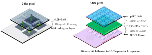 Concept of 3-tier µLED GaN pixel allowing an emissive array with strong pitch reduction thanks to 3DSI in combination with 3D hybrid bonding technology. CEA-Leti’s 400 °C CMOS process enables such top-tier integration without exceeding the thermal limits of the active circuitry below.
The team showed that SOI devices processed at 400 °C instead of the high temperature (>1000 °C) industry standard and high-temperature industrial reference, performed equivalent to high-temperature devices.
“The 400 °C process enables 3D sequential stacking on any bottom tier,” Noguet said. “It’s a huge step forward because it’s far more mature—reliable and scalable—than current low-temperature solutions, such as polycrystalline films, oxide semiconductors or carbon nanotubes.”
Protecting Circuitry on Bottom-Tier LayersCEA-Leti’s team demonstrated n- and p-type transistors matching the characteristics of conventional high-temperature CMOS devices, while staying within the ≤400 °C thermal budget required to preserve active circuitry in lower layers.
The process relies on an optimized 400 °C LPCVD deposition for amorphous silicon followed by NLA in the melt regime for dopant activation and diffusion—producing polycrystalline, low-resistance gates with excellent interface quality. In addition, NLA-SPER mastering enables dopant activation without diffusion leading to access resistance within specifications.
The post FAMES Pilot Line R&D Advances: 400°C CMOS Enables 3D Integration Goals appeared first on ELE Times.
Pages


![[link]](https://i.redd.it/nf5elqtd477g1.jpeg)
![[link]](https://i.redd.it/vhgrryyri17g1.png)
![[link]](https://i.redd.it/pdltuqfnvw6g1.jpeg)