
Feed aggregator
Why Cascading Chipsets and Fusion Testing Define the Next Era of Automotive Radar
Automotive radar systems have become a cornerstone of advanced driver-assistance systems (ADAS), enabling object detection, collision avoidance, blind-spot monitoring, and adaptive cruise control. As vehicle autonomy advances toward higher SAE levels, radars are evolving with greater resolution, longer range, and multi-object tracking capabilities. But with this leap in performance comes the pressing challenge: how to test these increasingly complex systems with the accuracy and repeatability needed for safe deployment on public roads.
Technology Environment: 24 GHz to 77 GHz and Higher:
The environment of automotive radar is changing quickly. Due to bandwidth constraints and stricter spectrum laws, traditional 24 GHz radars once common for short-range applications like parking assistance and cross-traffic alerts are currently being phased out.
Radars operating at 77 GHz are replacing them as the new norm. They provide a greater bandwidth, longer detection ranges, better range resolution, and more robust interference resistance. For mid- to long-range ADAS features like adaptive cruise control, lane-change assistance, and automated emergency braking, they are therefore essential. However, there is a cost and design complexity trade-off.
At the same time, radar sensing has evolved from 2D to 4D imaging radar. Conventional 2D radars could measure distance and velocity but lacked elevation, limiting object classification in dense traffic. By contrast, 4D imaging radars measure distance, velocity, azimuth, and elevation simultaneously producing LiDAR-like point clouds enriched with Doppler data. This technology thrives in poor weather conditions like fog, rain, or snow, where optical sensors struggle, making it indispensable for L2+ through L4 autonomy.
Radar Test Architecture:
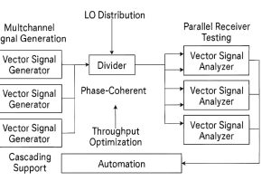
Radar Test Architecture for Automotive Applications: Phase-Coherent Multichannel Signal Generation, LO Distribution, and Parallel Receiver Testing with Automation Flow
This diagram illustrates a radar test setup optimized for automotive radar validation. It begins with multichannel vector signal generators that ensure phase coherence and support cascading for scalable configurations. The signals are routed through an LO distribution divider, feeding synchronized local oscillator signals to multiple vector signal analyzers for parallel receiver testing. At the base, an automation controller manages the test flow, enabling throughput optimization across channels.
Latest Trends in Radar Testing:
As radar performance expands, testing methodologies are transforming as well. Today’s radar testers are not only tasked with validation under ideal conditions but also with simulating real-world unpredictability before vehicles even hit the road.
- 4D Radar Simulation
Virtual test environments can replicate rain, snow, fog, and multipath reflections that are impractical to test on real roads. These simulations are vital for developing next-gen 4D radars.
- Hardware-in-the-Loop (HiL) Testing
HiL connects real radar hardware with a simulated driving environment. This allows engineers to test radar responses to cars, pedestrians, and traffic scenarios entirely in the lab—reducing cost and speeding up development.
- AI-Enhanced Radar Validation
AI plays an increasing role by detecting subtle anomalies in radar signals, generating rare accident-like scenarios, and predicting radar degradation. This accelerates validation cycles compared to manual testing.
- Sensor Fusion Testing
Since radars rarely operate alone, test systems now validate how radars integrate with cameras and LiDAR. Ensuring all sensors remain synchronized and error-free is critical to the safety of self-driving systems.
Industry Insights: Keysight Technologies at the Forefront
As automotive radar systems evolve to meet rising demands for higher resolution and precision, Keysight Technologies stands at the forefront of testing innovation. With chipset vendors adopting cascading architectures to boost transmit and receive channel counts, radar complexity is increasing alongside the need for more rigorous and extended test cycles. Natarajan Mahesh from Keysight’s Radar Testing Team highlights this shift as a key challenge in next-gen radar development.
“Automotive radar chipset vendors are looking to increase the transmit and receive channel count to cater to the increasing demand for better resolution using methods such as cascading radar chipsets. The higher channel count of receiver and transmitters will essentially mean more test time.” — Natarajan Mahesh, Radar Testing Team, Keysight Technologies
Keysight Technologies is addressing this challenge with specialized solutions that balance complexity with efficiency:
- Coherent Multichannel Signal Generators – providing compact, phase-aligned outputs with excellent phase noise.
- Local Oscillator Distribution – delivering stable, low-noise signals for cascading architectures.
- Simultaneous Multi-Channel Stimulus – enabling parallel receiver testing and cutting down test duration.
- Radar-Specific Test Automation – supporting MIMO radar, FMCW waveforms, and Doppler emulation.
Keysight also extends its scope into cybersecurity with its SA8710A Automotive Cybersecurity Test Platform, ensuring that radar systems in connected vehicles are validated not just for performance but also for resilience against digital threats.
“Keysight Technologies has solutions for the autonomous vehicle and in-vehicle communication systems, of which radar is one of the most critical sensors.”
 Natarajan Mahesh, Radar Testing Team, Keysight Technologies
Future Outlook:
- Fully Virtualized Validation: AI and physics-based simulations work together to provide nearly comprehensive test coverage prior to in-person trials.
- 5G-Connected Testbeds: over-the-air (OTA) firmware optimization and cloud-based radar analytics.
- Automated Test Labs: these robotic devices simulate targets dynamically from various perspectives.
- 4D radar standardization: frameworks for industry-wide certification that establish consistent performance benchmarks.
Conclusion:
Automotive radar testers are critical enablers of the next wave of ADAS and autonomy. As radars evolve from basic range-speed sensors to high-resolution 4D imaging systems, test platforms must evolve as well becoming simulation-rich, AI-driven, and fusion-aware.
Companies like Keysight Technologies are leading this transformation, ensuring that radar-equipped vehicles perform safely, reliably, and securely under all conditions ultimately paving the way toward fully autonomous driving.
The post Why Cascading Chipsets and Fusion Testing Define the Next Era of Automotive Radar appeared first on ELE Times.
Next-Gen EVs Run on Smarter, Smaller, and Faster Traction Inverters
Electric vehicles (EVs) are no longer defined merely by battery size or driving range. At the very heart of their performance, efficiency, and intelligence lies the traction inverter a masterpiece of power electronics that converts DC from the battery into precise AC waveforms for motor drive.
What makes the inverter even more critical today is its evolution into a software-defined energy hub. Beyond simple power conversion, modern inverters integrate advanced semiconductors, AI-driven control, and bidirectional energy flow, turning EVs into smart, grid-ready assets.
Technologies Reshaping Inverter Design:
- Wide-Bandgap Semiconductors: SiC and GaN
- The transition from traditional silicon to wide-bandgap (WBG) materials such as Silicon Carbide (SiC) and Gallium Nitride (GaN) is revolutionizing inverter efficiency and compactness.
- SiC MOSFETs support high-voltage (up to 1200 V) operation, offer lower switching losses, and provide high thermal endurance. This enables smaller form factors, decreases cooling system requirements, and facilitates ultra-fast charging.
- GaN HEMTs are known for their high-frequency switching, which makes e-axles and multilevel inverter topologies more compact. They’re emerging in light EVs and auxiliary systems where space is at a premium.
These devices can achieve switching frequencies above 500 kHz, unlocking higher power density and smaller passive components. While SiC has already become standard in 800 V platforms, GaN is set to complement it in next-gen EV systems.
- AI-Based Predictive Control
In the realm of inverters, artificial intelligence is ushering in new operational paradigms. With Model Predictive Control (MPC) and machine learning at the helm, contemporary inverters:
- Mitigate torque ripple and switching losses
- Adapt in real-time to driving dynamics, component wear, and thermal conditions
- Support over-the-air (OTA) updates, ensuring inverter functionality is fine-tuned for the vehicle’s entire lifespan
Furthermore, AI-augmented control integrates perfectly with battery management and regenerative braking systems, facilitating enhanced, safer, energy-efficient driving.
- 800 V Architectures: Faster, Cooler, Smarter
- The industry’s shift to 800 V platforms marks a significant leap in EV capability:
- Enables 200–350 kW ultra-fast charging with minimal I²R losses
- Reduces cable thickness and weight, improving efficiency
- Achieves 10–15 min charging to 80% capacity
In such high-voltage environments, SiC-based inverters thrive achieving >98% efficiency while maintaining robust thermal stability.
- Bidirectional Energy Flow: Beyond Mobility
Modern traction inverters are designed for four-quadrant operation, unlocking multiple use cases:
- Vehicle-to-Grid (V2G): Supplying power back to the grid
- Vehicle-to-Home (V2H): Acting as an emergency or renewable energy backup
- Vehicle-to-Load (V2L): Powering tools or appliances on the go
These applications require adherence to global standards like IEEE 1547 and ISO 15118, alongside isolation and fault-tolerance mechanisms. In effect, EVs are becoming mobile energy storage units, supporting energy resilience and sustainability.
- Integrated E-Axle Designs
OEMs are increasingly adopting integrated e-axle solutions that combine inverter, motor, and gearbox in a single compact package. Benefits include:
- Reduced parasitics and cabling losses
- Shared cooling and thermal management
- Lower manufacturing complexity and cost
This architecture improves torque density and space efficiency—ideal for both urban EVs and high-performance electric sports cars.
- Modular Inverter Architectures
Scalability is key for automakers producing EVs across different segments. Modular inverter platforms allow:
- Power scaling from 75 kW to 300 kW
- Reuse of software, control logic, and digital stages
- Faster time-to-market and lower R&D costs
This flexibility helps OEMs deploy multi-platform strategies, from two-wheelers to heavy-duty trucks, with automotive-grade reliability.
EV Traction Inverter Architecture:

Block diagram of an EV traction inverter system showing torque command flow from VCU to traction motor via Safe MCU, SiC FETs, gate drivers, and resolver-based feedback.
This diagram illustrates how torque commands from the Vehicle Control Unit (VCU) are processed by a safety-optimized microcontroller (Safe MCU), which drives high-voltage SiC FETs through isolated gate drivers. These switches convert DC from the battery into 3-phase AC for the traction motor. Resolver and current sensing provide real-time feedback, enabling precise motor control and efficient bidirectional energy flow.
System-Level Trends:
Beyond materials, traction inverter innovation is increasingly system-driven:
- Bidirectional Charging & V2G: SiC and GaN enable energy flow back to the grid, turning EVs into mobile storage units
- Integrated Powertrains: OEMs are combining inverter, motor, and gearbox into unified modules for space and weight savings
- Cooling Innovations: Double-sided cooling and optimized thermal paths are reducing module size and improving reliability
- Software-Defined Inverters: Adaptive control algorithms are enhancing efficiency across driving conditions
Industry Spotlight: Infineon Technologies
To understand how traction inverter technology is evolving in the EV sector, Hans Adlkofer, Senior Vice President of Automotive Systems at Infineon Technologies AG, shares his perspective. He explains the technological shifts driving more efficient, compact, and bidirectional inverters, and how these advancements are shaping the future of electric powertrains.
“We can expect even more compact and efficient traction inverter designs. The shift from traditional IGBTs to Silicon Carbide (SiC) is driven by the need for higher performance, reduced size, and increased EV range. Fusion of IGBT and SiC technologies in a single module also optimizes cost-performance. Gallium Nitride (GaN) will further support advanced inverter topologies, including multi-level designs.”
“The transition to SiC and GaN opens the space for innovative module development, such as smaller or optimized cooled modules. Discrete solutions allow very compact inverter designs or integration directly into the motor. This contributes to higher efficiency, lower cost, and increased mileage.”
“Latest SiC and GaN products enable bidirectional charging, supporting intelligent V2G use cases. EVs can now act as mobile energy storage units, creating a more sustainable energy ecosystem and new business models for battery utilization.”
 Hans Adlkofer, Senior Vice President Automotive Systems at Infineon Technologies AG
Conclusion:
Traction inverters are no longer functioning solely to change DC to AC traction inverters have effectively become the brain centre of an electric vehicle’s power train. They are changing electric vehicle performance and energy management with wide-band gap semiconductors, AI predictive control, modular system designs, and energy flow that is bidirectional.
As automakers focus on increasing charging speed, boosting range, and developing more intelligent energy systems, traction inverters will be instrumental in the renaissance of electric vehicles.
The post Next-Gen EVs Run on Smarter, Smaller, and Faster Traction Inverters appeared first on ELE Times.
Vishay Intertechnology Class 1 Radial-Leaded High Voltage Single Layer Ceramic Disc Capacitors Feature Low DC Bias and DF
Devices Reduce Power Losses in High Voltage Generators for Industrial and Medical Applications
Vishay Intertechnology, Inc. introduced a new series of Class 1 radial-leaded high voltage single layer ceramic disc capacitors that deliver a low dissipation factor (DF) and DC bias for industrial and medical applications.
Vishay Roederstein HVCC Class 1 series capacitors feature capacitance loss of < 25 % at 15 kV, which is half that of Class 2 devices. In addition, their < 1.0 % DF at 1 kHz is 0.5 % lower. The result is reduced power losses and high reliability in high voltage generators for baggage scanners, medical and industrial X-ray applications, air purifiers and ionizers, and pulsed lasers.
HVCC Class 1 series devices feature a capacitance range from 100 pF to 1 nF — with standard tolerances of ± 10 % — voltages of 15 kVDC, and an operating temperature range from -30 °C to +85 °C. The capacitors consist of a silver-plated ceramic disc with tinned copper-clad steel connection leads offering 0.65 mm and 0.80 mm diameters. The RoHS-compliant devices are available with straight leads with spacing of 9.5 mm and 12.5 mm, and feature an encapsulation made of flame-resistant epoxy resin in accordance with UL 94 V-0.
The post Vishay Intertechnology Class 1 Radial-Leaded High Voltage Single Layer Ceramic Disc Capacitors Feature Low DC Bias and DF appeared first on ELE Times.
MEMS and Modular Platforms Drive Breakthroughs in Audio Designs
My newly built workbench.
 | Just finished the major components of my workbench. Me and my girlfriend build the desk from scratch and i put my electronics in the room. Still got some tidying up to do and run power to the 3d-printer and lab bench power supply to the far left [link] [comments] |
ams OSRAM launches its first high-power multi-die laser package
UMass Lowell’s Anhar Bhuiyan wins two US NSF grants worth $797,000 for gallium oxide research
Choosing the Right Overcurrent Protection Device for Safe Consumer Designs
Low-cost NiCd battery charger with charge level indicator

Nickel Cadmium (NiCd) batteries are widely used in consumer electronics due to their high energy density and long life. Constant current charging is often recommended by manufacturers. Several websites, including Wikipedia, suggest safely charging NiCd batteries at a 0.1C rate, meaning at 10% of their rated capacity, for 14 to 16 hours, instead of 10 hrs.
Slow charging does not cause a temperature rise, which may affect the life of the battery. More energy must be supplied to the battery than its actual capacity to account for energy loss during charging. Hence, 14 to 16 hours of charging instead of 10 hours.
Wow the engineering world with your unique design: Design Ideas Submission Guide
The battery chargerFigure 1 gives the circuit for slow charging a NiCd battery pack with two AA-sized 1200-mAH cells. The battery is charged with 120 mA (10% of 1200 mA) constant current for about 15 hours.

Figure 1 The circuit for a low-cost NiCd (2 AA size 1200 mAH battery pack) slow charger with charge capacity indicator. Each segment in the U5 and U6 LED bar graphs indicates a charge capacity rise by 10%. As the charging current is constant, the time duration of charging indicates the charge capacity. After 10 hours, the battery should be fully charged. Charging for a few more hours than necessary supplies more energy to account for energy loss during charging. R2 and C1 are for the power ON reset of counters. The Vcc and ground pins of U2, U3, U7 and U8 are not shown here. They must be connected to 9-V DC and Vss, respectively. Time accuracy is not es. Each segment may glow for approximately 1 hour.
Every hour of charging is indicated by the glow of one LED bar graph segment (U5 and U6). After 15 hours, charging stops automatically. This is not a microcontroller-based circuit, so that even people without programming knowledge or a programmer device can build this circuit. A crystal-based timing circuit is not used here, as there is no necessity for time accuracy.
How it worksU1 is 555, configured as an astable multivibrator to generate a pulse train of width 0.88 seconds. R7 can be replaced by a 50K resistor and a 50K multiturn potentiometer in series for adjustment. LED D2 blinks at this rate.
U7 divides this pulse train. Dividing by a 212 output at pin one yields a pulse train with a pulse width of 1 hour. U2A counts these pulses.
U3 is a 4- to 16-line decoder with an active LOW output. The selected output goes LOW, causing the corresponding bar graph segment to glow, while all other outputs remain HIGH. Since the 16th output at pin 15 of U3 remains HIGH, Q1 turns ON and the battery starts charging, and D1 begins glowing.
U4 is configured as a constant current generator. With R3 set as 10 Ω, the charging current is set at 100 mA, which is 10% of 1200 mA.
During the first hour, the output of U3 at pin 11 goes LOW, and the first segment of the LED bar graph U5 glows. After 1 hour, counter U2A increments once, and the output of U3 at its pin 9 goes LOW, which causes the second segment of the LED bar graph (U6) to glow.
This process goes on until the 15th segment glows to indicate the 15th hour of charging. When the 16th hour starts, the 16th output at pin 15 of U3 goes LOW, turning Q1 OFF.
Now charging stops, and the “Charging ON” LED D1 goes OFF. This LOW output, connected to U8B inverter input, outputs HIGH at the U2A clock input, which disables further counting. Hence, Q1 continues to be OFF. At this point, the battery is fully charged and becomes ready for usage.
Jayapal Ramalingam has over three decades of experience in designing electronics systems for power & process industries and is presently a freelance automation consultant.
Related Content
- NiCd Battery Charger Circuit
- NiCd battery-reconditioning circuit restores aged rechargeable cells
- Two-wire interface has galvanic isolation
- Two-wire remote sensor preamp
- Tearing apart a multi-battery charger
- Proper Lithium-Ion battery charging and safety
The post Low-cost NiCd battery charger with charge level indicator appeared first on EDN.
Top 10 Decision Tree Learning Algorithms
Decision tree learning algorithms are supervised machine learning algorithms that solve classification and regression problems. These models split up data through branches based on feature values until at the very end, a prediction is made; this setup closely aligns with human decision logic. Each internal node represents a decision based on a feature, whereas each branch represents results of that decision, and each leaf corresponds to a final prediction or class label. This intuitiveness makes them easily interpretable and graphical, hence their application in various fields.
Types of decision trees learning algorithms:
Decision tree algorithms are varied according to how splits are conceived, what types of data they handle, and how computationally efficient they are. ID3 is the basic algorithm which splits or bifurcates depending upon information gain and works well for classification, though it tends to overfit and exhibits problems with continuous attributes from the get-go. Based on ID3, C4.5 adds gain ratio for more effectively dealing with discrete and continuous data, though it can struggle in noisy environments. CART is a general-purpose algorithm applied to both classification and regression; it optimizes Gini impurity for classification and mean squared error (MSE) for regression, and includes pruning for diminishing overfitting. CHAID uses chi-square tests for split and is best suited for large categorical data, although it’s not best for continuous variables. CART is extended by Conditional Inference Trees use statistical hypothesis testing to perform unbiased splits with multiple types of data but are generally slower than standard tree algorithms because they have stringent testing mechanisms.
Decision tree learning algorithms examples:
Decision trees find their applications in real-world instances. They diagnose diseases based on the symptoms in the healthcare system. They assess loan eligibility by considering income and credit score in finance. They forecast a particular weather condition based on factors such as temperature and humidity in meteorology. They recommend products based on the analysis of user behavior in e-commerce. They are versatile due to their ability and flexibility to work with numerical as well as categorical data.
Top 10 decision tree learning algorithms:
- ID3 (Iterative Dichotomiser 3)
ID3 is one of the earliest classes of decision tree algorithms, developed by Ross Quinlan. It uses the information gain to select the best feature on which to split the data at each instance of a node. The algorithm calculates entropy that signifies the impurity of a dataset and selects the feature that gives the largest decrease in entropy. ID3 is a very simple and elegant approach to classification problems. However, it suffers when dealing with continuous data. Also, ID3 does not work well in the presence of noise or when the training data is very small, as it tends to overfit the data.
- C4.5
C4.5 is an extension of the ID3 algorithm and solves many of its shortcomings. Most importantly, it introduces the “gain ratio” as a splitting criterion, so that information gain is normalized and is not biased toward features with many values. It also includes support for continuous attributes, pruning, and handling missing values, ideal features to make it robust and applicable to real-life datasets. It is one of the most influential algorithms in decision tree learning.
- CART (Classification and Regression Trees)
CART is an all-purpose medium for the classification and regression. They evaluate Gini impurity or sometimes called error, while regression uses Mean Squares Errors (MSE) to quantify the accuracy of splits. CART always grows binary trees; that is, each node can split exactly into two branches. It uses cost-complexity pruning to improve accuracy and avoid overfitting and hence, is widely used in modern ML.
- CHAID (Chi-squared Automatic Interaction Detector)
The chi-square tests determine the best splits, so this is best for categorical data and multiway splits. Unlike CART, CHAID can create trees with more than two branches per node. It’s particularly effective in market research, survey analysis, and social science applications, where categorical variables dominate. However, it’s less effective with continuous data and may require discretization.
- QUEST (Quick, Unbiased, Efficient Statistical Tree)
QUEST uses statistical tests to produce an unbiased and quick decision tree splitting. It can avoid the bias that some algorithms yield regarding the variable with many levels and is efficient in handling large datasets. QUEST accepts explanatory variables, either categorical or continuous, and provides pruning mechanisms. It is rarely used in preference to CART or C4.5 but is appreciated for its statistical rigor and for speed.
- Random Forest
Random Forest is an ensemble learning method where many trees are constructed using bootstrap samples and random sampling of features, and then each tree votes for the final prediction. This leads to better accuracy and less overfitting. It works well for classification and regression problems and handles large data sets with higher dimensions. Being fast, robust, and scalable, Random Forest is often used as a benchmark in predictive modeling.
- XGBoost (Extreme Gradient Boosting)
XGBoost works by sequentially building trees, with each one focusing on correcting the errors of the previous one by regularizing to avoid overfitting, and it is generally optimized for speed and performance. XGBoost has become a go-to algorithm in data science competitions due to its high accuracy and efficiency. It supports parallel processing and handles missing values gracefully.
- LightGBM (Light Gradient Boosting Machine)
LightGBM stands for Light Gradient Boosting Machine and is a speed- and scale-oriented gradient boosting algorithm developed by Microsoft. Using a leaf-wise tree growth strategy, LightGBM basically results in deeper trees and better accuracy. It is helpful when working with large datasets and supports categorical features natively. It is widely used across industries for various applications like fraud detection, recommendation systems, and ranking problems.
- Extra Trees (Extremely Randomized Trees)
The execution of Extra Trees resembles that of Random Forest, but more randomness is inducted as splitting thresholds are chosen at random and not optimized. This increases bias and reduces variance and may lead to faster training times. If your dataset is prone to overfitting, this method may be useful, and it is beneficial when dealing with high-dimensional data. In ensemble learning, Extra Trees are often employed to increase generalization.
- HDDT (Hellinger Distance Decision Tree)
HDDT uses the Hellinger distance as a splitting criterion, making it effective for imbalanced datasets. It’s particularly useful in domains like fraud detection and rare event modeling, where traditional algorithms may falter.
The post Top 10 Decision Tree Learning Algorithms appeared first on ELE Times.
Infineon releases 12kW high-density PSU reference design for AI data centers and servers
Workbench Wednesday
 | submitted by /u/SocialRevenge [link] [comments] |
Eulitha ships 6-inch-wafer DUV litho systems to several Asian VCSEL foundries
My finest bodge yet. 0.02mm (.0080")
") | I missed to route two traces from a Raspberry Pi Compute Module socket (my acrrier board) and had to rework. The pad has a width of 0.2mm (.0080"), so I got extra a new tip for that (Weller LT 1LX). After two attempts I could successfully tack the bodgewire to the unconnected pads. [link] [comments] |
Building the Smallest: Magnetic Fields Power Microassembly
As technology around us enters unconventional areas, such as rings and glasses, it is nothing but the marvels of miniaturization and microassembly redefining the rules. Miniaturization refers to the trend of making products and devices smaller, particularly in electronics, mechanics, and optics. Microassembly, on the other hand, is the precise manipulation, orientation, and assembly of microscale components, often smaller than 1000 micrometers, into complex, functional hybrid microsystems, such as those found in Microelectromechanical Systems (MEMS).
The two concepts, miniaturization and microassembly, are the most interconnected themes of the electronics industry, powering the next generation of technology revolution from homes to appliances and roads to vehicles. This vast application compels us to track and see what’s latest with the technology while also considering the challenges and opportunities the sector has to offer. Recent studies in the field of medical electronics have unveiled certain challenges that have led to the development of new micro-systems. The following article intends to unravel those very latest observations and developments.
What’s the problem with heterogeneous integration?
As the macroscopic devices are converted into their micro/nano-scale counterparts, integration of components like electronic devices, micro-electromechanical structures (MEMS), and optoelectronic devices on the same substrate is a debated issue. It is because of the different physical forces manifesting themselves in varying proportions owing to scaling effects.
For instance, adhesion forces that originate primarily from surface tension, van der Waals forces, and electrostatic forces are fundamental limitations of micromanipulation. In particular, the adhesion forces between objects are significant compared with the gravitational forces when the sizes of the components are less than 1 mm. This means that as the components, the target objects, become smaller, the surface-area-to-volume ratio increases, leading to a more pronounced scaling effect, hence originating difficulties in the fabrication of miniature devices.
All this is because the physical considerations change as we move from the macro- to the microscale. Earlier conducted studies have considerably shown that micro/nano-robots are sensitive to environmental parameters and that the dominant forces in different media are distinct (only van der Waals forces are ubiquitous).
As the scale decreases, objects invisible to the naked eye must be studied using light or electron microscopes. While the ability to control each object diminishes, their collective properties become more significant. These scale-dependent physical principles demand different strategies for designing devices at the micro- and nano-levels. Naturally, challenges that are straightforward at the macroscopic scale become far more complex in this domain.
As we move into exploring various domains using this technology, the design of microassembly/micromanipulation processes must consider these factors to isolate undesired interference, which is a challenging task in practice.
What is the solution?
According to a paper published in Elsevier’s Engineering Monthly, it discusses this very problem to reach a solution. The paper discusses various solutions, one of which is a multimer design by Yu et al., where the researcher combines several small pieces of different materials into a connected group. This makes sure that the nanoparticles that were earlier prone to sticking due to higher forces are prevented from tumbling end-over-end, which keeps changing the contact points. This dynamic motion reduces the time and area of contact, so sticking is weaker.
This logically translates into building components with different microscale components with different geometries and materials. Assembled devices, which are usually manipulated through non-covalent interactions, are responsive to environmental stimuli such as temperature, pressure, and flow. Eventually, the paper suggests using magnetic, optical, and acoustic fields and mechanical methods to generate actuation power at the micro/nano-scale.Additionally, owing to their rapid response and ability to be remotely controlled, magnetic field-based methods offer a pathway for one-dimensional (1D) to 3D microassembly.
While there are various ways, we’ll focus on electromagnetic principles only, for now. Magnetic field-induced assembly (MFIA) of nanoparticles allows for the 1D, two-dimensional (2D), or 3D organization of magnetic particles under the influence of a magnetic field. This refers to the automatic and spontaneous arrangement of particles within a magnetic field rather than an assembly induced by artificially moving targets. Experiments also show that under a uniform intensity of magnetic field, the nanoparticles arrange themselves in a linear, chain-like, or hexagonal pattern even in in vivo applications.
Hence, using an external magnetic field, programmed devices can be made, turning them into magnetically actuated microrobots. Using the same principle, magnetically controlled microrobots have been used for several different microassembly tasks. The assembled block, spherical, and flake-like magnetic doping devices can be used to assist robots in pushing different units for the assembly of micro components.
How does this improve grip & control?
Electromagnetic fields allow magnetic micro-units to be precisely controlled. By programming their magnetic response, these units can move in a directed way and assemble into desired structures or swarms. Temporary anchoring methods (like hydrogels or mechanical locks) prevent accidental movement, ensuring stability until assembly is complete. Advanced designs, such as quadrupole modules, also minimize interference between neighboring units. Together, these techniques improve both the precision of positioning and the grip or stability of micro-components during assembly.
Another approach to microassembly uses magnetic microgrippers that can hold and transport individual units. Unlike magnetic microrobots that mainly push components into place, microgrippers can grasp them directly, allowing for more precise and complex 3D assembly.
In conclusion, assembled magnetic microrobots demonstrate versatile and controllable propulsion under rotating magnetic fields, enabling functions such as transport, stirring, and targeted delivery. While artificial designs like magnetic microcubes showcase structured assembly for cell transport, biohybrid microrobots expand these possibilities by integrating magnetic materials with living cells. Such innovations, including macrophage-based robots capable of 3D navigation and drug delivery, highlight the growing potential of magnetic microrobots in advanced biomedical applications.
Applications
These microcomponents can form diverse geometries and can easily be decoupled as the magnetic field gradually dissipates. This flexibility in structural reorganization allows them to adapt to and overcome different environmental constraints. Expanding programmed magnetic assemblies to biological materials with programmed orientations and structures, the paramagnetism of radicals to biological materials has been used in order to endow magnetic assemblies of different arbitrariness with programmed orientations and structures.
Eventually, the use of magnetic devices provides the basis for the development of microbiotics. When these units become functional with closed-loop control, for instance, in drug delivery, they can be classified as microrobots rather than merely micro-patterned components.
Micro-assemblies with magnetic Microrobots: The application of an external magnetic field can both convert different components into programmed devices and turn them into magnetically actuated microrobots. This section summarizes the magnetic actuation and navigation of assembled micro-robots. These microrobots can be divided into two main types: magnetically actuated microrobots for robot-assisted assembly and assembled swimming magnetic microrobots as carriers or deliverers.
- Bio-inspired microrobots: Magnetically controlled bio-inspired microrobots have shown great potential in microassembly tasks. Different geometries—such as blocks, spheres, flakes, and cubes—enable them to push, grasp, or transport components in both fluid and solid environments.
- Magnetic Micro-Grippers: These are microassembly tools capable of grabbing and transporting units, enabling more sophisticated 3D assembly than pushing-based microrobots. Fabricated using techniques like digital light-processing 3D printing with magnetic and nonmagnetic resins, they can be remotely guided by magnetic fields to operate in confined spaces.
Assembled Swimming Magnetic Microrobots as Carriers or Deliverers: Assembled magnetic microrobots, driven by a rotating magnetic field, can achieve controllable propulsion in diverse fluidic environments. They can be configured into chain-like structures for transporting cells or act as microstirrers. Beyond artificial designs, biohybrid microrobots—such as macrophage-based systems or magnetotactic bacteria—enable precise drug delivery and cancer cell targeting. These cell-based microrobots, capable of forming dimers, trimers, or tetramers, respond to environmental cues like light, offering versatile and targeted delivery applications.
Prominent Challenges
While the technology holds immense potential, it also comes with some inherent challenges to counter. Some of them have been listed below:
- Miniaturization & Production: Space limits and scale mismatches require advanced methods like two-photon polymerization.
- Handling Fragile Objects: Flexible structures (e.g., neural electrodes) demand high precision; current methods are costly or lack accuracy.
- Feedback Limits: Visual systems fail in closed environments; alternatives include Fiber Bragg sensors, mini-endoscopes, and MRI-compatible robots.
- Automation: Over-reliance on vision reduces robustness; advanced strategies like reinforcement learning are needed for autonomous navigation.
- Safety: Metallic magnetic residue poses risks; biofriendly carriers help, but safe removal methods and standardized assessments are still lacking.
In conclusion, MFIA and magnetic microrobots provide versatile, remotely controlled tools for microassembly with strong potential in biomedical engineering. Their broader adoption and clinical use will depend on overcoming key challenges—practicality, complex geometries, reliable feedback in closed environments, higher automation, and material safety.
The post Building the Smallest: Magnetic Fields Power Microassembly appeared first on ELE Times.
TI unveils the industry’s most sensitive in-plane Hall-effect switch, enabling lower design costs
In-plane Hall-effect switch from TI can replace incumbent position sensors that are more expensive and difficult to manufacture
Texas Instruments (TI) introduced the industry’s most sensitive in-plane Hall-effect switch for position sensing, offering engineers a cost-effective, user-friendly alternative to magnetoresistive sensors. TI’s TMAG5134 Hall-effect switch features an integrated a magnetic concentrator, enabling it to detect magnetic fields as weak as 1mT in applications such as door and window sensors, personal electronics, home appliances, and more. This level of sensitivity allows for the use of smaller magnets, further reducing system-level costs. Additionally, the TMAG5134’s in-plane sensing capability enables it to detect magnetic fields parallel or horizontal to a printed circuit board, giving engineers greater design flexibility.
Why it matters
Engineers seeking high sensitivity levels in low-power, compact position-sensing designs today rely on reed switches or tunnel magnetoresistive (TMR), anisotropic magnetoresistive (AMR) or giant magnetoresistive (GMR) sensors. However, these technologies often come with high costs and manufacturing complexities because they require specialized materials and fabrication techniques. In contrast, Hall-effect technology eliminates the need for specialized manufacturing and enables engineers to significantly reduce design costs and speed time to market.
Historically, designers have not considered Hall-effect switches as viable replacements for TMR, AMR, GMR or reed switches because of their limited sensitivity. The introduction of TI’s TMAG5134 represents a fundamental shift for the position sensing market; engineers can now achieve greater sensitivity than traditional Hall-effect sensors without the additional cost and complexity of magnetoresistive sensors.
“The electronics we interact with in our daily lives, from our laptops to our smart home systems, use sensors to help make decisions based on the world around them,” said Jason Cole, vice president and general manager, Sensing Products at TI. “For decades, TI’s sensing portfolio has enabled engineers to achieve greater accuracy, power efficiency and reliability in their designs. The TMAG5134 Hall-effect switch builds on these years of innovation, delivering a simplified, cost-effective solution that creates new possibilities for design engineers across industries.”
The post TI unveils the industry’s most sensitive in-plane Hall-effect switch, enabling lower design costs appeared first on ELE Times.
ASDC Conclave 2025: Accelerating Tech-Driven Skilling for Future Mobility
Automotive Skills Development Council (ASDC) hosted its 14th Annual Conclave 2025, themed “Stronger Together, Transform Tomorrow”, bringing together leaders from government, industry, and academia to deliberate on the future of skilling in the automotive sector.
The event commenced with the traditional lamp lighting ceremony. F.R. Singhvi, President, ASDC, presented the Annual Update, highlighting the Council’s 2024–25 impact—key achievements included forging partnerships with universities, advancing women’s skill development and employment, strengthening industry–academia collaboration, and expanding its international footprint. This was followed by addresses from the Guests of Honour: C.S. Vigneshwar (President, FADA), Shradha Suri Marwah (CMD, Subros Limited & President, ACMA), C.V. Raman (CTO, Maruti Suzuki India Ltd.), and Dr. Vinita Aggarwal, IES (Retd.), Executive Member, NCVET.
C.V. Raman, CTO, Maruti Suzuki India Ltd, emphasized that India’s mobility future will be driven by advanced engineering, digitalization, and disruptive technologies such as EVs, IoT, and AI. To realize the $5 trillion vision, he stressed the need for skilling to evolve by integrating experiential learning, fostering industry–academia collaboration, and leveraging startup innovation.
Dr. Vinita Aggarwal highlighted the importance of qualification standardization, stating: “India’s journey to becoming a global skill hub is powered by standardization and industry alignment. With over 180 automotive QPs under NSQF, we must ensure they remain dynamic—integrating hands-on training, apprenticeships, and micro-credentials. The automotive sector should actively adopt and upgrade these QPs to build a future-ready, tech-driven workforce.”
Speaking at the conclave, F R Singhvi, President, ASDC, remarked: “This conclave has reinforced our belief that India’s skilling ecosystem thrives on partnerships. Together, we are shaping a workforce that is not only job-ready but future-ready.”
A major milestone of the conclave was the release of a White Paper and the signing of MoUs with Hero MotoCorp, Bajaj Auto, Gandhi Auto, Delphi TVS, and Bosch India to scale up skilling initiatives nationwide.
The conclave also hosted two high-impact panel discussions: Academic Excellence to Industry Impact: Aligning Talent Pipelines with Future Mobility Technologies and From Garage to Gigabyte: Skilling for Next-Gen Automotive Technologies. These sessions examined how new-age skilling can bridge classroom learning with the demands of digital-first, tech-driven automotive industries.
Vinkesh Gulati, Vice President, ASDC, added: “Our collective responsibility is to ensure that every young aspirant finds a place in the industry’s growth story. ASDC is committed to bridging the gap between potential and opportunity.”
The Certified Candidates Convocation felicitated skilled candidates from ASDC’s flagship programs, underscoring its commitment to inclusive skill development. Presentations on CSR Best Practices by Bajaj Auto and Hero MotoCorp Ltd. showcased impactful industry-led skilling models. Recognitions included Internationally Placed Candidates, Rewards & Recognition Awards, and the ASDC Excellence and Special Recognition Awards, celebrating exemplary contributions to the skilling ecosystem.
The conclave firmly reiterated that public-private partnerships will be the cornerstone in addressing the evolving needs of the automotive industry and enabling India to emerge as a global leader in mobility technologies.
The post ASDC Conclave 2025: Accelerating Tech-Driven Skilling for Future Mobility appeared first on ELE Times.
Making your architecture ready for 3D IC

The landscape of IC design is experiencing a profound transformation. With the physical and economic limits of conventional two-dimensional scaling, the industry is rapidly embracing three-dimensional integrated circuits (3D IC) to unlock higher performance, lower power consumption, and denser silicon utilization.
For semiconductor professionals, understanding the distinct nuances of 3D IC microarchitectures is no longer optional. It’s becoming essential for those seeking to maintain a competitive edge in next-generation system design.
Microarchitecting in the 3D IC era represents more than an incremental change from traditional practices. It entails a fundamental redefinition of how data and controls move through a system, how blocks are partitioned and co-optimized across both horizontal and vertical domains, and how early-stage design decisions address the unique challenges of 3D integration.
This article aims to provide essential context and technical depth for practitioners working toward highly integrated, efficient, and resilient 3D IC systems.

3D IC technology now stands at a pivotal juncture. Source: Siemens EDA
Putting things in context
To grasp the impact of 3D IC, it’s crucial to define microarchitecture in the IC context. System architecture typically refers to a design’s functional organization as seen by software engineers—abstract functions, data flows, and protocols. Microarchitecture, viewed through the hardware engineer’s lens, describes how those features are realized in silicon using components like register files, arithmetic logic units, and on-chip memory.
Microarchitecture centers around two domains: the datapath, which encompasses the movement and transformation of data, and the control, which dictates how and when those data movements occur. Together, they determine not only performance and efficiency but also testability and resiliency.
Furthermore, while traditional ICs optimize microarchitecture in two dimensions, 3D ICs require designers to expand their strategies into the vertical axis as well. Because data in 3D ICs no longer flows only laterally, it must be orchestrated through stacked dies, each potentially featuring its own process technology, supply voltage, or clock domain. Inter-die communication—typically realized with micro-bumps, through-silicon vias, or hybrid bonding—becomes critical for both data and control signals.
With the move toward submicron interconnection pitches, design teams must address tighter integration densities and the unprecedented task of partitioning logic and memory across multiple vertical layers. This process is not unlike assembling a three-dimensional puzzle.
Effective microarchitecture in this context demands careful co-optimization of logic, physical placement, routing, and inter-die signaling—with far-reaching implications for system latency, bandwidth, and reliability.
Moreover, some microarchitectural components can be realized in three dimensions themselves. Stacked memory sitting directly above compute units, for example, enables true compute-in-memory subsystems, affecting both density and performance but also introducing significant challenges related to signal integrity, thermal design, and manufacturing yield.
Taking complexity to the third dimension
A major trend shaping modern IC development is the shift toward software-defined silicon, where software can customize and even dynamically control hardware features. While this approach provides great flexibility, it also increases complexity and requires early, holistic consideration of architectural trade-offs—especially in 3D ICs, where the cost of late-stage changes is prohibitive.
The high costs of 3D IC design and manufacturing in general demand an upfront commitment to rigorous partitioning and predictive modeling. Errors or unforeseen bottlenecks that might be addressed after tape-out in traditional design can prove disastrous in 3D ICs, where physical access for rework or test is limited.
It is thus essential for system architects and microarchitects to collaborate early, determining both physical placement of blocks and the allocation of functionality between programmable and hardwired components.
This paradigm also introduces new questions, such as which features should be programmable versus fixed? And how can test coverage and configurability be extended into the post-silicon stage? Design teams must maintain a careful balance among performance, area, power, and system flexibility as they partition and refine the design stack.
Among the most significant physical challenges in 3D integration is the sharp increase in power density. Folding a two-dimensional design into a 3D stack compresses the area available for power delivery, while escalating local heat generation. Managing thermal issues becomes significantly more difficult, as deeper layers are insulated from heat sinks and are more susceptible to temperature gradients.
Test and debug also become more complex. As interconnect pitches shrink below one-micron, direct probing is not practical. Robust testability and resilience need to be designed in from the architecture and circuit level, using techniques like embedded test paths, built-in self-test, and adaptive power management long before finalization.
Finally, resiliency—the system’s ability to absorb faults and maintain operation—takes on new urgency. The reduced access for root-cause analysis and repair in 3D assemblies compels development of in-situ monitoring, adaptive controls, and architectural redundancy, requiring innovation that extends into both the digital and analog realms.
The need for automation
The complexity of 3D IC design can only be managed through next-generation automation. Traditional automation has centered on logic synthesis, place and route, and verification for 2D designs. But with 3D ICs, automation must span package assembly, die stacking, and especially multi-physics domains.
Building 3D ICs requires engineers to bridge electrical, thermal, and mechanical analyses. For instance, co-design flows must account for materials like silicon interposers and organic substrates. This necessitates tightly integrated EDA tools for early simulation, design-for-test verification, and predictive analysis—giving teams the ability to catch issues before manufacturing begins.
System heterogeneity also sets 3D IC apart. Diverse IP, technology nodes, and even substrate compositions all coexist within a single package. Addressing this diversity, along with long design cycles and high non-recurring engineering costs, demands multi-domain, model-based simulation and robust design automation to perform comprehensive early validation and analysis.
Meanwhile, traditional packaging workflows—often manual and reliant on Windows-based tools—lag far behind the automated flows for silicon IC implementation. Closing this gap and enabling seamless integration across all domains is essential for realizing the full promise of 3D IC architectures.
The evolving role of AI and design teams
As system complexity escalates, the industry is shifting from human-centered to increasingly machine-centered design methodologies. The days of vertical specialization are yielding to interdisciplinary engineering, where practitioners must understand electrical, mechanical, thermal, and system-level concerns.
With greater reliance on automation, human teams must increasingly focus on oversight, exception analysis, and leveraging AI-generated insights. Lifelong learning and cross-functional collaboration are now prerequisites for EDA practitioners, who will require both broader and more adaptable skillsets as design paradigms continue to evolve.
Artificial intelligence is already transforming electronic design automation. Modern AI agents can optimize across multiple, often competing, objectives—proposing floorplans and partitioning schemes that would be unfeasible for manual evaluation. Looking ahead, agentic AI—teams of specialized algorithms working in concert—promise to orchestrate ever more complex design sequences from architecture to verification.
Building failure resilient systems
As the boundaries between architectural roles blur, collaboration becomes paramount. In a world of software-defined silicon, architects, microarchitects, and implementation engineers must partner closely to ensure that design intent, trade-offs, and risk mitigation are coherently managed.
Real-world progress is already visible in examples like AMD’s 3D integration of SRAM atop logic dies. Such hybrid approaches demand careful analysis of read and write latency, since splitting a kernel across stacked dies can introduce undesirable delays. Partitioning memory and processing functions to optimize performance and energy efficiency in such architectures is a delicate exercise.
Heterogeneous integration also enables new microarchitectural approaches. High-performance computing has long favored homogeneous, mesh-based architectures, but mobile and IoT applications may benefit from hub-and-spoke or non-uniform memory access models, requiring flexible latency management and workload distribution.
Adaptive throttling, dynamic resource management, and redundancy strategies are growing in importance as memory access paths and their latencies diverge, and architectural resiliency becomes mission critical.
As failure analysis becomes more complex, designs must include real-time monitoring, self-healing, and redundancy features—drawing upon proven analog circuit techniques now increasingly relevant to digital logic.
Thermal management presents fresh hurdles as well: thinning silicon to expose backside connections diminishes its native lateral thermal conductivity, potentially requiring off-die sensor and thermal protection strategies—further reinforcing the need for holistic, system-level co-design.
3D IC moving forward
3D IC stands at a pivotal juncture. Its widespread adoption depends on early, multi-disciplinary design integration, sophisticated automation, and a holistic approach to resiliency. While deployment so far has largely targeted niche applications, such as high-speed logic-memory overlays, 3D IC architectures promise adoption across more segments and vastly more heterogeneous platforms.
For industry practitioners, the challenges are formidable, including three-dimensional partitioning, integrated automation across disciplines, and entirely new approaches to test, debug, and resilience. Meeting these challenges requires both technical innovation and significant organizational and educational transformations.
Success will demand foresight, tight collaboration, and the courage to rethink assumptions at every step of the design cycle. Yet the benefits are bountiful and largely untapped.
 Todd Burkholder is a senior editor at Siemens DISW. For over 25 years, he has worked as editor, author, and ghost writer with internal and external customers to create print and digital content across a broad range of EDA technologies. Todd began his career in marketing for high-technology and other industries in 1992 after earning a Bachelor of Science at Portland State University and a Master of Science degree from the University of Arizona.
 Pratyush Kamal is director of Central Engineering Solutions at Siemens EDA. He is an experienced SoC and systems architect and silicon technologist providing technical leadership for advanced packaging and new foundry technology programs. Pratyush previously held various jobs at Google and Qualcomm as SoC designer, SoC architect, and systems architect. He also led 3D IC research at Qualcomm, focusing on both wafer-on-wafer hybrid bond and monolithic 3D design integrations.
Editor’s Note
This is the first part of the three-part article series about 3D IC architecture. The second part, to be published next week, will focus on how design engineers can put 3D IC to work.
Related Content
- 3D IC Design
- Thermal analysis tool aims to reinvigorate 3D-IC design
- Heterogeneous Integration and the Evolution of IC Packaging
- Tighter Integration Between Process Technologies and Packaging
- Advanced IC Packaging: The Roadmap to 3D IC Semiconductor Scaling
The post Making your architecture ready for 3D IC appeared first on EDN.
Top 10 Reinforcement Learning Algorithms
Reinforcement Learning (RL) algorithms represent a class of machine learning methodologies where an agent learns to make decisions through interactions with an environment. The agent gets feedback in the form of rewards or punishments bestowed on it for the actions it takes, and the overall objective is to maximize cumulative rewards through time. Differing from supervised learning, RL does not rely upon labeled data, but rather it learns from experience. Through trial and error, reinforcement learning excels at solving sequential decision-making problems across domains like robotics, gaming, and autonomous systems especially when using value-based algorithms that estimate future rewards to guide action.
Main types of Reinforcement Learning (RL) algorithms:
- Value-Based Algorithms
Value-based algorithms primarily work towards evaluating the potential benefits an action may have in a given condition while making a decision. Value-based methods usually learn a value function known as the Q-value, which specifies the expected reward in the future by taking a particular action in a certain state. The agent executes an action with the aim of maximizing this value. An example of such algorithms is the Q-Learning algorithm wherein Q-values are updated through the Bellman equation. More advanced versions are Deep Q-Networks (DQN) that approximate these values by using neural networks in high-dimensional environments such as video games.
- Policy-Based Algorithms
Policy-based algorithms directly learn a policy that maps states to actions without estimating value functions. These methods optimize the policy using techniques like gradient ascent to maximize expected rewards. They are particularly useful in environments with continuous action spaces. One popular example is REINFORCE, a Monte Carlo-based method. Another widely used algorithm is Proximal Policy Optimization (PPO), which improves training stability by limiting how much the policy can change at each update.
3. Model-Based Methods:
These algorithms learn the model and simulate the evolution of states from an initial state and finally an action. Once the dynamics model is learned, the agent can use it to simulate the future states and choose the best action without ever interacting with the real environment. This family of algorithms is very sample-efficient and suitable for cases where acquiring data is either very costly or risky. An example that revolutionized the field is MuZero, which learns the model and the policy without ever being given the rules of the environment;at the same time, it attains state-of-the art performance in Go, Chess, and other board games.
4. Actor-Critic Algorithms
Actor-Critic algorithms are a hybrid reinforcement learning technique that combine the advantages of both value-based and policy-based methods. Actor-critic methods maintain two perspectives: the actor decides what action to take, while the critic evaluates how good the action was by employing a value function. This idea of two perspectives given stability to the training process and fosters great performance. Examples of algorithms: Advantage Actor-Critic(A2C), Asynchronous Advantage Actor-Critic(A3C), and Soft Actor-Critic (SAC) These are typically used in continuous control problems such as in robotics and autonomous driving.
Examples of Reinforcement Learning Algorithms:
Some widely used RL algorithms are Q-Learning, Deep Q-Networks (DQN), Proximal Policy Optimization (PPO), and Soft Actor-Critic (SAC). Q-Learning is a basic algorithm that learns the value of actions in discrete environments. On the other hand, DQN uses deep neural networks to work with high-dimensional inputs such as images and videos. PPO is a policy-based algorithm known for its stability and efficiency in continuous control tasks and hence is often applied in robotics. SAC is an actor-critic method that uses entropy regularization to promote exploration and thus achieves a very good performance in brutally difficult environments.
Top 10 reinforcement learning algorithms:
- Q-Learning
Since it is a value-based algorithm, Q-Learning is ideal for discrete action spaces. It learns by receiving rewards with which it updates Q-values for optimal action-selection policy. This makes it ideal, for example, in simple setups such as grid-worlds or basic games.
- Deep Q-Network (DQN)
DQN is an extension of Q-Learning in which Q-values are approximated using deep neural networks, enabling it to handle high-dimensional inputs such as raw pixels. It has had a great impact on RL by offering a solution for agents to play Atari games straight from screen images.
- Double DQN
Double DQN improves DQN by reducing overestimation bias through decoupled action selection and evaluation, resulting in more stable learning.
- Dueling DQN
Dueling DQN extends DQN by splitting the state value estimation and action advantage estimation, which is particularly beneficial for problems with many similar actions.
- Proximal Policy Optimization (PPO)
PPO is a policy algorithm that is both stable and efficient. It employs a clipped objective to avoid sudden policy updates and thus performs well in continuous control tasks such as robotics and locomotion.
- Advantage Actor-Critic
Advantage Actor-Critic is policy and value learning combined, which makes it applicable to real-time decision-making in dynamic, multi-agent environments.
- Deep Deterministic Policy Gradient (DDPG)
DDPG is geared for continuous action spaces and employs a deterministic policy gradient algorithm. It’s best applied to tasks such as robotic arm control and autonomous vehicles, where accuracy matters when it comes to actions.
- Twin Delayed DDPG (TD3)
TD3 improves DDPG with the addition of twin critics to mitigate overestimation and policy update delay for improved stability. These features make it particularly suitable for high-precision control in difficult simulations.
- Soft Actor-Critic (SAC)
SAC promotes exploration with the incorporation of an entropy bonus to the reward signal. This allows the agent to strike a balance between exploration and exploitation, making it extremely sample-efficient and powerful in deep exploration-requiring environments.
- MuZero
MuZero is a model-based algorithm that learns an environment model without knowing its rules. It unifies planning and learning to deliver state-of-the-art performance on strategic games such as Chess, Go, and Atari, and it’s one of the most sophisticated RL algorithms to exist.
The post Top 10 Reinforcement Learning Algorithms appeared first on ELE Times.
Now, where's that diode?!
 | [Not mine] [link] [comments] |
Pages


![[link]](https://i.redd.it/kbofrnc9ydof1.jpeg)
![[link]](https://i.redd.it/isoagv43tbof1.jpeg)
![[link]](https://i.redd.it/9fb9fpqkjbof1.jpeg)
![[link]](https://i.redd.it/zi0uv2wabaof1.jpeg)