
Feed aggregator
ams OSRAM and Nichia expand their intellectual property collaboration
ams OSRAM extends CFO Rainer Irle’s contract until 2030
Photon Design showcasing laser simulation tool developments at Optica Laser Congress
Microchip’s SkyWire Tech Enables Nanosecond-Level Clock Sync Across Locations
To protect critical infrastructure systems, SkyWire technology enables highly scalable and precise time traceability to metrology labs
Network clocks are the backbone of critical infrastructure operations, with the precise alignment of clocks becoming increasingly important for data centers, power utilities, wireless and wireline networks and financial institutions. For critical infrastructure operators to deploy timing architectures with reliability and resiliency, their clocks and timing references must be measured and verified to an authoritative time source such as Coordinated Universal Time (UTC). Microchip Technology announced its new SkyWire technology, a time measurement tool embedded in the BlueSky Firewall 2200, that is designed to measure, align and verify time to within nanoseconds even when clocks are long distances apart.
With the BlueSky GNSS Firewall 2200 and SkyWire technology, geographically dispersed timing systems can be compared to each other and compared to the time scale systems deployed at metrology labs within nanoseconds. Measurement of clock alignment and traceability to this level has typically only been done between metrology labs and scientific institutes. With Microchip’s solution, critical timing networks for air traffic control, transportation, public utilities and financial services can achieve alignment within nanoseconds between its clocks to protect their infrastructure no matter where the clocks are located.
“To ensure timing systems are delivering to stringent accuracy requirements, it’s important to measure and verify in an independent manner relative to UTC as managed by national laboratories and traceable to the Bureau International Poids et Mesures (BIPM),” said Randy Brudzinski, corporate vice president of Microchip’s frequency and timing systems business unit. “With the new SkyWire technology solution, we’re making UTC more widely accessible so that large deployments of clocks can be independently measured and verified against each other across long distances.”
The concept originated as an extension to the National Institute of Standards and Technology’s (NIST’s) pre-existing service called Time Measurement and Analysis Service (TMAS), which is utilized by entities that are required to maintain an accurate local time standard. The BlueSky GNSS Firewall 2200 with SkyWire technology provides a Commercial Off-The-Shelf (COTS) product to enable critical infrastructure operators to connect with the NIST TMAS Data Service for large-volume clock deployments.
“At NIST, our goal is to enable the most accurate time to support our country’s infrastructure,” said, Andrew Novick, engineer at NIST. “Our TMAS Data Service in conjunction with commercial hardware, provides a scalable solution for anyone who needs traceable and accurate timing.”
Nations around the globe can replicate this solution using Microchip’s SkyWire technology capabilities within its TimePictra software suite, which delivers similar features and functionality as that provided by the NIST TMAS Data Service. Metrology labs, government agencies and enterprises worldwide can deploy TimePictra software suite and the BlueSky GNSS Firewall 2200 with SkyWire technology and have their own end-to-end solution for traceable time measurement, alignment and verification.
The post Microchip’s SkyWire Tech Enables Nanosecond-Level Clock Sync Across Locations appeared first on ELE Times.
Next Generation Hybrid Systems Transforming Vehicles
The global automotive industry is undergoing a fundamental transformation moving from internal combustion engines (ICEs) to electric and hybrid vehicles that redefine mobility as sustainable, intelligent, and efficient.
This shift is not merely regulatory-driven; it’s fueled by a shared pursuit of carbon neutrality, cost-effectiveness, and consumer demand for cleaner mobility options.
Hybrid electric technology has proven to be the most practical bridge to date between traditional combustion and complete electrification. Providing the versatility of twin propulsion — electric motor and ICE — hybrid powertrains give the advantages of fuel economy, lower emissions, and a smoother transition for both consumers and manufacturers.
From regenerative braking to capture kinetic energy to AI-enabled energy management optimizing power delivery, hybrids are the sophisticated union of software and engineering. As countries pledge net-zero, and OEMs retool product strategies, hybrid technology is not merely a transition measure — it’s the strategic foundation of the auto decarbonization agenda.
Innovations Driving Hybrid Systems
- Solid-State & Next-Gen Lithium-Ion Batteries
Next-generation solid-state batteries hold the potential for greater energy density, quicker charging, and increased safety. Their ability to double the energy storage capacity and halve the charging time makes it a game-changer for hybrid and plug-in hybrid vehicles.
- Regenerative Braking & E-Axle Integration
Regenerative braking captures kinetic energy and converts it into electricity during braking, pumping it back into the battery. Coupled with e-axle technology, this integration optimizes drivetrain efficiency and performance.
- Lightweight Composites for Higher Efficiency
Advances in carbon-fiber-reinforced plastics and aluminum alloys allow automakers to shave weight, increase efficiency, and enhance range — all without sacrificing safety.
- AI-Powered Energy Management Systems
Artificial intelligence is now at the heart of hybrid optimization — learning driving habits, anticipating power needs, and controlling energy transfer between engine, motor, and battery for optimum efficiency.
Industry Insights: Mercedes-Benz on Hybrid Innovation
Rahul Kumar Shah, Senior Engineer at Mercedes-Benz Research & Development, outlines the engineering philosophy behind the company’s next-gen hybrid powertrains.
“At Mercedes-Benz, we view hybridisation not as an interim solution, but as a masterclass in energy orchestration. Our focus is on creating a seamless dialogue between the combustion engine and electric motor — ensuring the right power source is deployed at the right time to deliver maximum efficiency and a signature Mercedes driving experience.”
Optimizing Hybrid Powertrain Architectures:
“We have advanced from conventional parallel systems to sophisticated P2 and P3 architectures. By placing high-torque electric motors strategically within the drivetrain, we eliminate turbo lag and allow smaller, thermally efficient combustion engines to deliver spirited performance. Combined with predictive AI energy management, our vehicles decide in real time whether to operate in electric mode, recharge, or blend both power sources for optimal efficiency.”
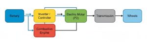
Figure (1)
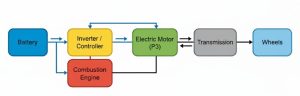
Figure (2)
The P2 Hybrid (first diagram) places the electric motor between the engine and transmission, allowing it to drive the wheels directly alongside the engine or independently. The P3 Hybrid (second diagram) places the electric motor on the transmission output shaft, leveraging greater torque multiplication but coupling the electric drive to the transmission output shaft. Both are Parallel PHEVs using a battery and inverter to manage power flow to the wheels.
Regenerative Braking:
“Our eDrive motors can decelerate the car up to 3 m/s² using purely regenerative energy. Coupled with our ESP HEV system, regenerative and mechanical braking are blended seamlessly to ensure vehicle stability and natural pedal feel. Integration with navigation and radar allows the vehicle to preemptively harvest energy — effectively ‘sailing on electricity.”
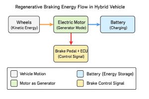
During regenerative braking, the wheels’ kinetic energy is converted by the motor (in generator mode) into electrical energy, which charges the battery. This process is triggered by a control signal from the brake pedal and ECU.
Thermal Management:
“Managing heat across the combustion engine, electric motor, and battery is essential. We maintain optimal battery temperatures between 20–40°C and reuse waste heat for cabin and coolant heating, reducing overall energy draw and improving efficiency.”
Solid-State Batteries:
“For hybrids, the real advantage lies in power density and durability. Solid-state cells can deliver and absorb charge much faster, enabling more efficient regenerative braking and smoother electric boosts. They are set to become the ultra-durable heart of next-generation hybrid powertrains.”
The Future of Hybrid Powertrains
The hybrid era is entering a smarter, cleaner, and more connected phase. Over the next decade, hybrid systems will evolve from being a bridge technology to a core pillar of sustainable mobility.
- Plug-in Hybrids Take Center Stage
Plug-in hybrids (PHEVs) will lead the transition, providing longer electric-only ranges and rapid charging. With bi-directional charging (V2G), they’ll also supply homes or return energy to the grid, making vehicles portable energy centers.
- Hydrogen Enters the Hybrid Mix
Hybrid powertrains assisted by hydrogen will appear, particularly in commercial and long-distance vehicles. Blending fuel cell stacks with electric drives, they will provide zero-emission mobility with rapid refueling and long range.
- Modular Electric Platforms
At-scale automakers are shifting to scalable modular architectures that integrate the battery, e-axle, and drive unit into flexible “skateboard” configurations. These platforms will reduce their costs and enable software-defined performance updates through over-the-air upgrades.
- AI-Optimized Energy Management
Artificial intelligence will power real-time power delivery, anticipating traffic and terrain to balance efficiency with performance. Future hybrids will be able to learn, adjust, and self-optimize, combining intelligence with propulsion.
- Smart Materials & Circular Manufacturing
The hybrids of tomorrow will be lighter and cleaner — constructed from recycled composites, graphene-reinforced metals, and bio-based plastics. Closed-loop recycling will enable hybrid production to become more sustainable from start to finish.
Conclusion

Hybrid powertrains are no longer a bridge they’re becoming the cornerstone of an intelligent, networked mobility ecosystem.
As electrification grows and carbon-neutral goals firm up, hybrids will become smarter, self-tuning systems that efficiently couple combustion with electric precision.
Next-generation hybrid platforms will talk to smart grids, learn from the behavior of drivers, and self-regulate energy across varying propulsion sources from batteries to hydrogen cells. Optimization using AI, predictive maintenance, and cloud-based analytics will transform vehicles into operating modes, charging, and interacting with their surroundings.
Hybrids aren’t just a bridge—they’re the bold intersection where combustion and electrification unite to rewrite the future.
The post Next Generation Hybrid Systems Transforming Vehicles appeared first on ELE Times.
TI launches power management devices for AI computing

Texas Instruments Inc. (TI) announced several power management devices and a reference design to help companies meet AI computing demands and scale power management architectures from 12 V to 48 V to 800 VDC. These products include a dual-phase smart power stage, a dual-phase smart power module for lateral power delivery, a gallium nitride (GaN) intermediate bus converter (IBC), and a 30-kW AI server power supply unit reference design.
“Data centers are very complex systems and they’re running very power-intensive workloads that demand a perfect balance of multiple critical factors,” said Chris Suchoski, general manager of TI’s data center systems engineering and marketing team. “Most important are power density, performance, safety, grid-to-gate efficiency, reliability, and robustness. These factors are particularly essential in developing next-generation, AI purpose-driven data centers, which are more power-hungry and critical today than ever before.”
 (Source: Texas Instruments Inc.)
Suchoski describes grid-to-gate as the complete power path from the AC utility gird to the processor gates in the AI compute servers. “Throughout this path, it’s critical to maximize your efficiency and power density. We can help improve overall energy efficiency from the original power source to the computational workload,” he said.
TI is focused on helping customers improve efficiency, density, and security at every stage in the power data center by combining semiconductor innovation with system-level power infrastructure, allowing them to achieve high efficiency and high density, Suchoski said.
Power density and efficiency improvementsTI’s power conversion products for data centers address the need for increased power density and efficiency across the full 48-V power architecture for AI data centers. These include input power protection, 48-V DC/DC conversion, and high-current DC/DC conversion for the AI processor core and side rails. TI’s newest power management devices target these next-generation AI infrastructures.
One of the trends in the market is a move from single-phase to dual-phase power stages that enable higher current density for the multi-phase buck voltage regulators that power these AI processors, said Pradeep Shenoy, technologist for TI’s data center systems engineering and marketing team.
The dual-phase power stage has very high-current capabilities, 200-A peak, Shenoy said, and it is in a very small, 5 × 5-mm package that comes in a thermally enhanced package with top-side cooling, enabling a very efficient and reliable supply in a small area.
The CSD965203B dual-phase power stage claims the highest peak power density power stage on the market, with 100 A of peak current per phase, combining two power phases in a 5 × 5-mm quad-flat no-lead package. With this device, designers can increase phase count and power delivery across a small printed-circuit-board area, improving efficiency and performance.
Another related trend is the move to dual-phase power modules, Shenoy said. “These power modules combine the power stages with the inductors, all in a compact form factor.”
The dual-phase power module co-packages the power stages with other components on the bottom and the inductor on the top, and it offers both trans-inductor voltage regulator (TLVR) and non-TLVR options, he added. “They help improve the overall power density and current density of the solution with over a 2× reduction in size compared with discrete solutions.”
The CSDM65295 dual-phase power module delivers up to 180 A of peak output current in a 9 × 10 × 5-mm package. The module integrates two power stages and two inductors with TLVR options while maintaining high efficiency and reliable operation.
The GaN-based IBC achieves over 1.5 kW of output power with over 97.5% peak efficiency, and it also enables regulated output and active current sharing, Shenoy said. “This is important because as we see the power consumption and power loads are increasing in these data centers, we need to be able to parallel more of these IBCs, and so the current sharing helps make that very scalable and easy to use.”
The LMM104RM0 GaN converter module offers over 97.5% input-to-output power conversion efficiency and high light-load efficiency to enable active current sharing between multiple modules. It can deliver up to 1.6 kW of output power in a quarter-brick (58.4 × 36.8-mm) form factor.
TI also introduced a 39-kW dual-stage power supply reference design for AI servers that features a three-phase, three-level flying capacitor power-factor-correction converter paired with dual delta-delta three-phase inductor-inductor-capacitor converters. The power supply is configurable as a single 800-V output or separate output supplies.
 30-kW HVDC AI data center reference design (Source: Texas Instruments Inc.)
TI also announced a white paper, “Power delivery trade-offs when preparing for the next wave of AI computing growth,” and its collaboration with Nvidia to develop power management devices to support 800-VDC power architectures.
The solutions will be on display at Open Compute Summit (OCP), Oct. 13–16, in San Jose, California. TI is exhibiting at Booth #C17. The company will also participate in technology sessions, including the OCP Global Summit Breakout Session and OCP Future Technologies Symposium.
The post TI launches power management devices for AI computing appeared first on EDN.
The progression of wafer sizes through the years at the fab I work at.
 | 3 inch to 8 inch. Fab has been around since the 60s. Currently the 8 inch is our production size but the 6 inch is still used in the company and they float around as engineering wafers. [link] [comments] |
My humble workbench
 | My simple lab in my dungeon. Recently picked up the Kepco Programmable Power Supply and Agilent 54622D oscilloscope from work. We’re moving buildings and they’re tossing a lot of stuff. I’m running an Intel NUC with Win11, HP Slice with Fedora, RPi 4b (in the 3D printed green and black Fractal case) with RPi OS, and a Dogbone running Debian. It’s a very simple setup compared to a lot of yours but I love it. A nice place to escape. [link] [comments] |
100-V GaN transistors meet automotive standard

Infineon Technologies AG unveils its first gallium nitride (GaN) transistor family qualified to the Automotive Electronics Council (AEC) standard for automotive applications. The new CoolGaN automotive transistor 100-V G1 family, including high-voltage (HV) CoolGaN automotive transistors and bidirectional switches, meet AEC-Q101.
 (Source: Infineon Technologies AG)
This supports Infineon’s commitment to provide automotive solutions from low-voltage infotainment systems addressed by the new 100-V GaN transistor to future HV product solutions in onboard chargers and traction inverters. “Our 100-V GaN auto transistor solutions and the upcoming portfolio extension into the high-voltage range are an important milestone in the development of energy-efficient and reliable power transistors for automotive applications,” said Johannes Schoiswohl, Infineon’s head of the GaN business line, in a statement.
The new devices include the IGC033S10S1Q CoolGaN automotive transistor 100 V G1 in a 3 × 5-mm PQFN package, and the IGB110S10S1Q CoolGaN transistor 100 V G1 in a 3 × 3-mm PQFN. The IGC033S10S1Q features an Rds(on) of 3.3 mΩ and the IGB110S10S1Q has an Rds(on) of 11 mΩ. Other features include dual-side cooling, no reverse recovery charge, and ultra-low figures of merit.
These GaN e-mode power transistors target automotive applications such as advanced driver assistance systems and new climate control and infotainment systems that require higher power and more efficient power conversion solutions. GaN power devices offer higher energy efficiency in a smaller form factor and lower system cost compared to silicon-based components, Infineon said.
The new family of 100-V CoolGaN transistors target applications such as zone control and main DC/DC converters, high-performance auxiliary systems, and Class D Audio amplifiers. Samples of the pre-production automotive-qualified product range are now available. Infineon will showcase its automotive GaN solutions at the OktoberTech Silicon Valley, October 16, 2025.
The post 100-V GaN transistors meet automotive standard appeared first on EDN.
Бібліотечний проєкт "Збережи історію КПІ" триває: подаровані видання і колекції

Уже кілька років у бібліотеці відбуваються різноманітні заходи в рамках проєкту "Збережи історію КПІ ім. Ігоря Сікорського" – проводяться цикли лекцій, організуються засідання круглих столів, тематичні книжкові виставки та створюються спеціальні інсталяції.
Voltage-to-period converter offers high linearity and fast operation

The circuit in Figure 1 converts the input DC voltage into a pulse train. The period of the pulses is proportional to the input voltage with a 50% duty cycle and a nonlinearity error of 0.01%. The maximum conversion time is less than 5 ms.
 Figure 1 The circuit uses an integrator and a Schmitt trigger with variable hysteresis to convert a DC voltage into a pulse train where the period of the pulses is proportional to the input voltage.
Wow the engineering world with your unique design: Design Ideas Submission Guide
The circuit is made of four sections. The op-amp IC1 and resistors R1 to R5 create two reference voltages for the integrator.
The integrator, built with IC2, RINT, and CINT, generates two linear ramps. Switch S1 changes the direction of the current going to the integrating capacitor; in turn, this changes the direction of the linear ramps. The rest of the circuit is a Schmitt trigger with variable hysteresis. The low trip point VLO is fixed, and the high trip point VHI is variable (the input voltage VIN comes in there).
The signal coming from the integrator sweeps between the two trip points of the trigger at an equal rate and in opposite directions. Since R4 = R5, the duty cycle is 50% and the transfer function is as follows:
![]()
To start oscillations, the following relation must be satisfied when the circuit gets power:
![]()
Figure 2 shows that the transfer function of the circuit is perfectly linear (the R² factor equals unity). In reality, there are slight deviations around the straight line; with respect to the span of the output period, these deviations do not exceed ± 0.01%. The slope of the line can be adjusted to 1000 µs/V by R2, and the offset can be easily cancelled by the microcontroller (µC).

Figure 2 The transfer function of the circuit in Figure 1. It is very linear and can be easily adjusted via R2.
Figure 1 shows that the µC converts period T into a number by filling the period with clock pulses of frequency fCLK = 1 MHz. It also adds 50 to the result to cancel the offset. The range of the obtained numbers is from 200 to 4800, i.e., the resolution is 1 count per mV.
Resolution can be easily increased by a factor of 10 by setting the clock frequency to 10 MHz. The great thing is that the nonlinearity error and conversion time remain the same, which is not possible for the voltage-to-frequency converters (VFCs). Here is an example.
Assume that a voltage-to-period converter (VPC) generates pulse periods T = 5 ms at a full-scale input of 5 V. Filling the period with 1 MHz clock pulses produces a number of 5000 (N = T * fCLK). The conversion time is 5 ms, which is the longest for this converter. As we already know, the nonlinearity is 0.01%.
Now consider a VFC which produces a frequency f = 5 kHz at a 5-V input. To get the number of 5000, this signal must be gated by a signal that is 1 second long (N = tG * f). Gate time is the conversion time.
The nonlinearity in this case is 0.002 % (see References), which is five times better than VPC’s nonlinearity. However, conversion time is 200 times longer (1 s vs. 5 ms). To get the same number of pulses N for the same conversion time as the VPC, the full-scale frequency of the VFC must go up to 1 MHz. However, nonlinearity at 1 MHz is 0.1%, ten times worse than VPC’s nonlinearity.
The contrast becomes more pronounced when the desired number is moved up to 50,000. Using the same analysis, it becomes clear that the VPC can do the job 10 times faster with 10 times better linearity than the VFCs. An additional advantage of the VPC is the lower cost.
If you plan to use the circuit, pay attention to the integrating capacitor. As CINT participates in the transfer function, it should be carefully selected in terms of tolerance, temperature stability, and dielectric material.
Jordan Dimitrov is an electrical engineer & PhD with 30 years of experience. Currently, he teaches electrical and electronics courses at a Toronto community college.
Related Content
- Voltage-to-period converter improves speed, cost, and linearity of A-D conversion
- Circuits help get or verify matched resistors
- RMS stands for: Remember, RMS measurements are slippery
References:
- AD650 voltage-to-frequency and frequency-to-voltage converter. Data sheet from Analog Devices; www.analog.com
- VFC320 voltage-to-frequency and frequency-to-voltage converter. Data sheet from Burr-Brown; www.ti.com
The post Voltage-to-period converter offers high linearity and fast operation appeared first on EDN.
“Flip ON Flop OFF” for 48-VDC systems with high-side switching

My Design Idea (DI), “Flip ON Flop OFF for 48-VDC systems,“ was published and referenced Stephen Woodward’s earlier “Flip ON Flop OFF” circuit. Other DIs published on this subject matter were for voltages less than 15 V, which is the voltage limit for CMOS ICs, while my DI was intended for higher DC voltages, typically 48 VDC. In this earlier DI, the ground line is switched, which means the input and output grounds are different. This is acceptable to many applications since the voltage is small and will not require earthing.
However, some readers in the comments section wanted a scheme to switch the high side, keeping the ground the same. To satisfy such a requirement, I modified the circuit as shown in Figure 1, where input and output grounds are kept the same and switching is done on the positive line side.

Figure 1 VCC is around 5 V and should be connected to the VCC of the ICs U1 and U2. The grounds of ICs U1 and U2 should also be connected to ground (connection not shown in the circuit). Switching is done in the high side, and the ground is the same for the input and output. Note, it is necessary for U1 to have a heat sink.
Wow the engineering world with your unique design: Design Ideas Submission Guide
In this circuit, the voltage dividers R5 and R7 set the voltage at around 5 V at the emitter of Q2 (at VCC). This voltage is applied to ICs U1 and U2. A precise setting is not important, as these ICs can operate from 3 to 15 V. R2 and C2 are for the power ON reset of U1. R1 and C1 are for the push button (PB) switch debounce.
When you momentarily push PB once, the Q1-output of the U1 counter (not the Q1 FET) goes HIGH, saturating the Q3 transistor. Hence, the gate of Q1 (PMOSFET, IRF 9530N, VDSS=-100 V, IDS=-14 A, RDS=0.2 Ω) is pulled to ground. Q1 then conducts, and its output goes near 48 VDC.
Due to the 0.2-Ω RDS of Q1, there will be a small voltage drop depending on load current. When you push PB again, transistor Q3 turns OFF and Q1 stops conducting, and the voltage at the output becomes zero. Here, switching is done at the high side, and the ground is kept the same for the input and output sides.
If galvanic isolation is required (this may not always be the case), you may connect an ON/OFF mechanical switch prior to the input. In this topology, on-load switching is taken care of by the PB-operated circuit, and the ON/OFF switch switches zero current only, so it does not need to be bulky. You can select a switch that passes the required load current. While switching ON, first close the ON/OFF switch and then operate PB to connect. While switching OFF, first push PB to disconnect and operate the ON/OFF switch.
Jayapal Ramalingam has over three decades of experience in designing electronics systems for power & process industries and is presently a freelance automation consultant.
Related Content
- Flip ON Flop OFF
- To press ON or hold OFF? This does both for AC voltages
- Flip ON Flop OFF without a Flip/Flop
- Elaborations of yet another Flip-On Flop-Off circuit
- Another simple flip ON flop OFF circuit
- Flip ON Flop OFF for 48-VDC systems
The post “Flip ON Flop OFF” for 48-VDC systems with high-side switching appeared first on EDN.
Tobii and STMicroelectronics enter mass production of breakthrough interior sensing technology
Tobii and STMicroelectronics announced the beginning of mass production of an advanced interior sensing system for a premium European carmaker. It integrates a wide field-of-view camera, capable of seeing in daylight and at night with next-level driver and occupant monitoring, pushing the boundaries of user experience and safety.
“We’re very proud to bring this ground breaking system to life. This is more than just technology; it’s a vision,” said Adrian Capata, senior vice president of Tobii Autosense. “Image quality is critical, and thanks to our strong collaboration with ST, we’ve achieved a unique balance that allows a single-camera solution to meet rigorous safety standards, while also unlocking enhanced user experiences. By combining visible and IR sensing, we’re enabling intelligent in-cabin environments that truly understand human presence, behavior, and context.”
“As a result of close collaboration on development and integration with Tobii, we have created a new generation of interior sensing technology that is reliable, user-friendly, and ready for widespread adoption across the automotive industry,” said Alexandre Balmefrezol, Executive Vice President and General Manager of the Imaging Sub-Group at STMicroelectronics. “We are now rapidly expanding our production capacity to meet the anticipated demand and ensure a seamless transition to mass manufacturing.”
Technical information on the interior sensing system
Tobii’s and ST’s integrated approach allows automotive OEMs to install just one camera inside the cabin, providing the most mature, efficient, and cost-effective solution available on the market.
The system combines Tobii’s attention-computing technology with STMicroelectronics’ VD1940, an advanced image sensor designed primarily for automotive applications. This sensor features a single 5.1MP hybrid pixel design, sensitive to both RGB (colour in daytime) and infrared (IR at night time) light. Its wide-angle field of view covers the entire cabin, delivering exceptional image quality. Tobii’s algorithms process dual video streams to support both the Driver Monitoring System (DMS) and Occupancy Monitoring System (OMS).
The VD1940 image sensor is part of the SafeSense by ST, an advanced sensing technology platform designed by STMicroelectronics for DMS and OMS, which embeds functional safety and cyber security features and is dedicated to automotive safety applications. With this innovative product portfolio, ST is delivering reliable, high-quality, and cost-effective solutions tailored to the automotive industry. As an Integrated Device Manufacturer (IDM), STMicroelectronics masters the complete image sensor supply chain, with full control over both design and manufacturing processes. This ensures supply security through production of its imaging solutions in its European fabs, with these devices already in mass production and ready for integration by Tier 1s and OEMs.
The post Tobii and STMicroelectronics enter mass production of breakthrough interior sensing technology appeared first on ELE Times.
Infineon’s PQC-certified contactless and dual-interface security controller supports a quantum-safe world
Quantum computers are expected to become powerful enough within the next decade to compromise many of today’s cryptographic algorithms, putting a wide range of systems at risk. Long-life products such as ePassports, IoT devices and Secure Elements, therefore, demand post-quantum cryptography (PQC)-ready hardware already today. To address this, Infineon Technologies AG is providing the SLC27 security controller with a Common Criteria-certified cryptography library featuring the PQC algorithms ML-KEM and ML-DSA. As part of the TEGRION security controller family and based on the Integrity Guard 32 security architecture, the SLC27 supports standardized PQC implementations across multiple applications, enabling OEMs to integrate quantum-resistant security into their designs.
“At Infineon we know that quantum computing has the power to change the world because we are innovating in this field, too,” says Thomas Rosteck, Division President Connected Secure Systems at Infineon. “As quantum capabilities move from theory to reality, post‑quantum cryptography is an urgent, practical necessity — and Infineon is leading the industry in delivering certified, easy‑to‑adopt quantum‑resilient security that helps accelerating quantum resistance for crucial applications.”
Since post-quantum cryptography represents a fundamentally new class of cryptographic techniques, involving highly diverse and complex operations, it is essential to utilize a robust and security-optimized hardware platform. The SLC27 security controller, built on the Integrity Guard 32 security architecture, provides a resilient foundation for implementing high-performant PQC, excellently protected against side-channel and fault attacks. The controller also supports in-field updates and crypto agility, enabling OEMs to deploy PQC-ready hardware today and adapt to future requirements without replacing devices already in use. With these features, the SLC27 is suitable for applications where long device life and high security requirements demand quantum-resistant protection:
- IoT devices: Industrial sensors, smart meters, and control units often operate for ten to twenty years. The SLC27 allows such devices to remain protected against future quantum attacks throughout their operational lifetime.
- eID and ePassports: Government-issued ePassports and national eID cards with a typical ten-year validity can be future-proofed by integrating the SLC27, maintaining protected identification and border control systems.
- Secure Elements and brand protection: Secure Elements and brand protection solutions for luxury goods, health care devices and consumables benefit from PQC-enabled SLC27 to resist tampering and counterfeiting over the long term.
The post Infineon’s PQC-certified contactless and dual-interface security controller supports a quantum-safe world appeared first on ELE Times.
Navitas supporting 800VDC power architecture for NVIDIA’s next-gen AI factory computing platforms
Alpha and Omega Semiconductor supports 800VDC power architecture
NUBURU receives warning letter from NYSE American
Rohde & Schwarz unveils compact MXO 3 oscilloscopes with 4 and 8 channels
Rohde & Schwarz expands its next-generation MXO oscilloscope portfolio with the compact four- and eight-channel MXO 3 series. The MXO 3 delivers fast and precise advanced MXO technology – previously available only in larger, higher-priced models – in an extremely compact form factor at a more affordable price point. This oscilloscope allows engineers to see more of their device under test’s signal than any other instrument in this class.
Fast:
All MXO 3 models come standard with up to 99 % real-time capture, which is up to 50 times better than competitors’ instruments, enabling users to instantly see more signal details and rare events. Like other MXO models, these oscilloscopes leverage cutting-edge MXO-EP processing ASIC technology developed by Rohde & Schwarz to deliver:
- 5 million acquisitions per second– the fastest in the industry, allowing users to instantly detect additional signal detail and infrequent events.
- 600,000 trigger events per second with zone triggering– the fastest and most flexible in the industry, enabling users to isolate events in the time domain, including math and frequency domain signals.
- 50,000 FFTs per second– up to 1,000 times faster than other oscilloscopes, providing faster and more comprehensive analysis for applications such as EMI and harmonic testing.
- 600,000 math operations per second– the best in the industry and up to 100,000 times faster than competitive models, allowing users to accurately analyze signals like power, which require multiplication of voltage and current.
Precise:
All MXO 3 models are engineered with advanced technology to ensure accurate measurement isolation and results users can trust:
- 12-bit vertical resolutionin hardware at all sample rates allows users to observe small signal changes even of larger signals. This provides 16 times more resolution than traditional 8-bit oscilloscopes.
- HD modeenhances signal details that would otherwise be buried in noise. It offers both noise reduction and up to 18 bits of vertical resolution – the highest in the industry. Unlike other oscilloscopes, HD mode operates at full sample rate and is implemented in hardware, ensuring precision without sacrificing speed.
- With the largest offset range in its class, MXO 3 users can take advantage of the most sensitive vertical scale setup to reveal more of their signal while minimizing measurement system noise. MXO 3 oscilloscopes feature a wide ±3V offset at 1 mV/div on both 50 Ω and 1 MΩ input paths – two to three times better than other leading models in this class.
Compact:
Both the four- and eight-channel MXO 3 oscilloscopes are designed with a compact, portable form factor, making them easy to fit anywhere even on crowded benches. Their small footprint allows more space for the creative chaos of engineering workspaces. Combined with an industry-leading low audible noise – quieter than a whisper – the MXO 3 ensures a distraction-free work environment.
- 6” full-HD capacitive touchscreen, combined with intuitive user interface, offering an enhanced user experience to engineers who spend significant time working with the instrument
- Its light weight of only about 4 kg allows moving the MXO 3 easily to a different measurement location.
- 5U of rack height, ensuring efficient use of limited space in labs or testing environments.
- The VESA mountingcompatibility of the MXO 3 allows additional flexibility in engineering environments.
Philip Diegmann, Vice President of Oscilloscopes at Rohde & Schwarz, says: “With the launch of the MXO 3, we are bringing the breakthrough capabilities of our MXO technology to a more accessible, smaller instrument class. This compact oscilloscope delivers the same cutting-edge performance and usability that our customers have come to expect, while opening up new possibilities for engineers at a variety of price points, especially with the addition of an eight-channel model – the only instrument of its kind in this class. At Rohde & Schwarz, we are committed to making advanced test and measurement tools available to more users, and our fast, precise and compact MXO 3 is another step forward in that mission.”
The post Rohde & Schwarz unveils compact MXO 3 oscilloscopes with 4 and 8 channels appeared first on ELE Times.
🎥 У КПІ ім. Ігоря Сікорського презентували японські інноваційні рішення для відбудови України

На майданчику нашого університету відбулася демонстрація новітніх систем дистанційного управління від японських компаній Soliton і KOBELCO, що дозволяють керувати будівельною технікою віддалено — з дому, офісу, з будь-якої точки світу.
11 років тому в Україні стартували антикорупційні реформи

🇺🇦 Наша держава запровадила безпрецедентні за свою історію заходи для боротьби з корупцією, які й досі не вдалося втілити більшості пострадянських країн.
Pages


![[link]](https://i.redd.it/xj8i5reducvf1.jpeg)
![[link]](https://i.redd.it/igf8hbhwjcvf1.jpeg)