


Feed aggregator
A Raspberry Pi Camera Mounted on a Hat
A wearable video camera can be built with a Raspberry Pi 5 and a camera module, all enclosed in a case that attaches to a hat. The project was created to record video while moving without holding anything in your hands. The board runs the Broadcom BCM2712 quad-core processor at 2.4 GHz with Arm Cortex-A76 architecture, and the 2 GB RAM version is sufficient to handle the video stream.
The assembly is shown in the reference video. The source shows how to connect the camera module to the board and how to arrange everything inside the case. Anyone following the video will find the main steps without having to look elsewhere.
The board and the camera moduleThe Raspberry Pi 5 is the fifth generation from the Raspberry Pi Foundation. The 2 GB RAM version uses the Broadcom BCM2712 processor, a quad-core 2.4 GHz chip with Arm Cortex-A76 architecture. This configuration handles the camera module without any issues, and the module connects directly to the board.
The camera module goes into a black plastic case designed specifically for it. The case can sit on a flat surface or be attached with Velcro. The second option is the one needed for the hat: the Velcro keeps everything steady even when walking or running.
The case and the attachmentThe Raspberry Pi Camera Module case is a piece of black plastic that protects the lens and the circuit. Its shape is designed to be compact and comfortable on a hat. The Velcro included in the package lets you attach and detach it in seconds.
Only a few tools are needed for the assembly. The Velcro is cut to the right size and applied both to the case and to the hat fabric. Then the camera module is inserted into the case and the flat ribbon cable is connected to the board’s port.
The result is a lightweight camera that is not intrusive. You can use it for hikes, to document work, or to record a driving session. Video quality depends on the camera module and the light, but the board is never the bottleneck.
- Raspberry Pi 5 with 2 GB RAM
- Raspberry Pi Camera Module
- Black plastic case for the camera module
- Velcro for attachment
- Hat or flat surface
The list above summarizes the essential components. The Raspberry Pi 5 and the camera module are the two main pieces. The case and the Velcro complete the system and make it wearable.
The project also adapts to other uses. The same case with Velcro can be attached to a backpack, a bicycle, or a helmet. The board stays the same; only the mounting surface changes.
For those who want to go deeper, the reference video shows the assembly step by step. The source is especially useful for anyone who has never worked with a Raspberry Pi and needs to see the connections live.
Source: https://youtu.be/Hn-ClS2fmMU?si=BrOk84blJevP5YHU
The post A Raspberry Pi Camera Mounted on a Hat appeared first on Open Electronics.
FPGA architecture: SEU detection and recovery strategies

Part 1 of this mini-series covering single event upset (SEU) challenges in FPGA architectures examined radiation particles and related SEU challenges for FPGA applications that require robustness and predictability in ground-based and terrestrial applications.
Part 2 of the mini-series will cover SEU detection, recovery, and validation for FPGAs used in mission-critical systems such as aerospace, defense, telecommunications, and industrial applications.
Detection and recovery from SEUs require a layered strategy that addresses the distinct vulnerabilities of configuration RAM (CRAM), user logic, and embedded data storage. No single technique provides comprehensive coverage across all FPGA resource types. Instead, an effective approach combines complementary methods, each targeting a specific failure mode, with recovery mechanisms that are tightly coupled to the detection events that trigger them.
The following sections describe the detection techniques and their associated recovery strategies, from configuration-layer monitoring to logic-level redundancy to system-level behavioral observation.
CRAM readback and scrubbing
CRAM readback is the most basic detection technique for SEUs in CRAM. The system calculates a cyclic redundancy check (CRC) for the bitstream. An internal hardened configuration block in the FPGA reads back the CRAM contents and compares the calculated CRC to the expected result. If the results don’t match, the system can set a status flag to alert the user, for example via an internal interrupt to a soft processor or an external pin to a system-level board controller.
If the system flags an SEU error, the user can take action, for example:
- Stop the FPGA application and reload the bitstream, overwriting the CRAM to fix the flipped bit.
- Wait for an accumulation of SEUs before halting the application and reloading the bitstream.
- In some applications, it may be acceptable to power cycle the board and thereby the FPGA, which automatically reloads the bitstream upon power-up.
SEU scrubbing is another SEU recovery technique. Some FPGAs contain blind scrubbing circuits that run in the background and can periodically rewrite the entire bitstream regardless of whether the system detects an error. It’s easy to implement blind scrubbing because it does not require comparison logic; the downside is that blind scrubbing cannot give diagnostics on error rates and specific locations of SEU.
You can schedule scrubbing continuously or for a fixed period, depending on the application and trade-offs on additional power utilization. At terrestrial levels, you can usually set scrubbing intervals further apart, while at higher elevations, given the higher probability of radiation particles, intervals should be shorter.
More advanced SEU readback scrubbing circuits can detect and fix SEUs and report multiple upsets within a bitstream frame. Recent FPGA architectures have bitstreams that have frames that program subsets of the CRAM. Each frame is protected with single error correction and double error detection (SECDED). The SEU readback scrubbing circuit reads the contents of the CRAM and compares the calculated error correction code (ECC) for each frame with a known good ECC for that frame.
If the comparison fails, the circuit can locate the single bit failure based on the ECC mismatch signature and re-write the bitstream frame with the incorrect bit corrected. The SEU readback circuit is more complex and can give better diagnostics for error rates and failure locations. If the readback detects multiple uncorrectable errors however, you may need to reload the entire bitstream or power cycle the FPGA.
Error detection and correction for block RAM
Block RAM upsets require a dedicated detection and correction strategy because the stored data changes dynamically during operation and cannot be protected by static configuration scrubbing. Data written to RAM is wider by a certain number of bits, depending on the data width and encoding used for protection.
If you use an ECC encoder when writing data to RAM, you can use an ECC decoder when reading from RAM to detect corruption. ECC encoders and decoders can detect and correct single- and double-bit errors. From a system design perspective, using ECC to protect block RAM adds latency for encoding and decoding.
Some FPGAs have in-silicon ECC encoders for writing to the RAM and ECC decoders for reading from the RAM to detect and correct corrupted bits. These hardware-based encoders/decoders use more silicon area, have higher power, and have additional output delays. Implementing ECC encoding and decoding in your RTL design is a good option if few block RAMs are used for critical functions such as soft processor program memory, high integrity data paths, or state machine storage.
Triple modular redundancy (TMR)
TMR is the most robust mitigation strategy to guard against SEU errors. TMR requires three independent copies of a circuit to produce the same output. Each circuit has its own copy of combinational and sequential logic. The system compares the result from all three circuits, and two out of the three must match. This method provides a correct result even if one circuit is corrupted.
TMR provides continuous cycle-to-cycle error masking without any detection latency, and is very effective for protecting state machines, control logic, and safety-critical signal paths. However, TMR requires very strict architectural implementation to guarantee that none of the circuits share logic or routing with each other.
Although robust, TMR comes with a large trade-off in terms of FPGA resource usage and power. You need to use at least three times the resources to accommodate the triple redundancy and plan on higher power requirements as a result. Additionally, TMR cannot self-correct a bit error. A bit flip in one of the circuits continues to be corrupt until CRAM scrubbing can address the corruption.
Measuring SEU rates in FPGAs
Quantifying the reliability of an FPGA’s exposure to SEU can be done with specific testing using particle beam accelerators in specialized facilities. The standard figure of merit for terrestrial SEU rate is the soft error rate (SER) expressed in failures in time (FIT), where one FIT equals one failure per 10⁹ device hours.
Most FPGA manufacturers that support SEU detection and scrubbing reserve time at reputable facilities that can provide high energy beams of heavy ions, neutrons, protons, and alpha particles. Facilities can be found in the U.S., Canada, Switzerland, and Japan. This ground-based approach for accelerated testing helps to characterize the FPGA family’s radiation sensitivity. FIT data from the testing helps predict upset rates in target environments.
Ground-based testing and analytical modeling provide pre-deployment FIT rate estimates, but operational monitoring during deployment in the application environment provides the most accurate characterization of device behavior. CRAM detection and scrubbing circuits can log time, location, and frequency of detected SEUs, which you can compare to pre-deployment predictions.
If you observe rates that differ from pre-deployment predictions, you can redesign critical circuits, change scrubbing intervals, and/or change operational range. Most FPGA users work closely with their FPGA vendor to understand measured ground-based FIT rates from beam testing within a specific family and compare it to the application environment testing results.
FPGAs with SEU capabilities
Take the case of Efinix’s Titanium and Topaz families that are built on TSMC’s 16-nm FinFET process. These FPGAs benefit from the inherent SEU sensitivity advantages of the FinFET geometry relative to planar 2D transistor architectures at equivalent geometry.
These FPGas have characterized SEU behavior through independent testing conducted per JEDEC Std. JESD89A for alpha particles and per STd. JESD89 and JESD89-A for neutron particles, providing design engineers with measured FIT data from which you can determine system-level reliability.
The company’s Titanium FPGAs have CRAM SEU detection that lets design engineers monitor configuration integrity and respond to detected upsets through external recovery actions. Efinix also provides data on the FIT contribution from SEU events (transient failure rate) in a soft-error rate (SER) report.
Design engineers can use this data to determine whether on-chip mitigation features are required to achieve target Probabilistic Metric for random Hardware Failures (PMHF) values under ISO 26262-5 for their specific ASIL level.
Next, Titanium Edge FPGAs pair SEU detection capability with hardware scrubbing. The scrubbing architecture implements SECDED on a per-frame basis, operating at clock rates up to 80 MHz. SECDED enables automatic single-bit error correction without an external processor, and it flags uncorrectable double-bit errors for system-level response.
The SEU detection is configurable to meet different application needs. Automatic detection cycles through CRAM frames without user intervention, providing the lowest mean time to detection and the highest assurance of configuration integrity. Manual monitoring allows you to initiate a scrub cycle on demand.
Similarly, you can set detection and correction triggering as automatic, manual, or fixed-rate operation, tailoring the scrubbing interval to your deployment environment’s potential SEU rate. To support design validation and test system robustness, Titanium Edge FPGAs include a hardware error injection capability that can inject a single-bit error at any location within the CRAM array.
Finally, Topaz FPGAs have similar SEU detection capabilities as the Titanium family, but they don’t have the Titanium Edge scrubbing architecture overhead. System designers can monitor detected SEU errors and recover from them via an external action. This family is targeted at high-volume applications such as machine vision, industrial robotics, and broadcast imaging and controls.
Why SEU detection is critical
Radiation-induced SEUs represent a reliability challenge in modern FPGA design and technology. SEUs can silently flip bits that corrupt configuration memory, embedded memory, routing, and logic, thereby negatively impacting system behavior.
The threat to smaller process geometry FPGAs affects terrestrial applications as well as ground-based applications where thousands of FPGAs may be deployed in a system. Ground-based FIT rates may be low for a single FPGA, but when thousands are deployed, the probability of SEU impacting system behavior may increase to a level that requires detection and recovery.
Packaging technology advancements to reduce trace radioactive impurities and alpha particle emission have helped FPGA vendors reduce FIT rates. However, heavy ions, protons, and neutrons continue to expose FPGA vulnerabilities and require heavy beam testing to quantify the sensitivity to SEU and resulting FIT rates.
Detecting SEUs and scrubbing FPGA CRAM are critical to quantify an accumulation of errors that may require a reconfiguration or power cycle. Similarly, quantifying SEU errors within a specific altitude profile can guide systems on scrubbing cycle time by analyzing system power trade-offs versus expected error rates.
You must also analyze the trade-offs when planning for embedded block RAM protection. Error detection and correction require a lot of logic resources that could be soft or hardened in silicon. If you don’t need to detect and correct errors in all block RAM, a soft implementation for mission-critical block RAM can save power and resource utilization.
The most comprehensive strategy to protect against critical control and data path errors is TMR, but with a heavy cost of three times the resources and additional power. Alternatively, some applications may use a mix of TMR, block RAM ECC, and CRAM SEU detection and scrubbing.
No matter which method you choose for mitigating SEU exposure, it’s important to work with the FPGA vendor to understand their testing methodology and resulting FIT rate data. The FPGA FIT rate data can then be extrapolated to understand and compare actual measurements with the application profile.
 Mik Ichiba is principal field applications engineer at Efinix. He is a seasoned semiconductor and embedded systems professional with more than 30 years of experience spanning hardware architecture, PCB design, ASIC development, FPGA architecture, and system-level engineering. Throughout his career, Mik has worked across the hardware design lifecycle, helping organizations translate complex technical requirements into practical, high-performance solutions.
Editor’s Note
This is Part 2 of the mini-series about SEU challenges in FPGA architectures. Part 1 covered SEU radiation particles and related SEU challenges for FPGA applications that require robustness and predictability in ground-based and terrestrial applications.
Related Content
- Using FPGAs in mission-critical systems
- Rethinking the Logic-Routing Tradeoff in FPGAs
- Understanding Single Event Effects (SEEs) in FPGAs
- Enhancing robust SEU mitigation with 28-nm FPGAs
- Learn about SEU Immunity in Terrestrial FPGA Applications
The post FPGA architecture: SEU detection and recovery strategies appeared first on EDN.
Texas Instruments Showcases EV and Sustainable Energy Semiconductor Innovations at electronica India 2026
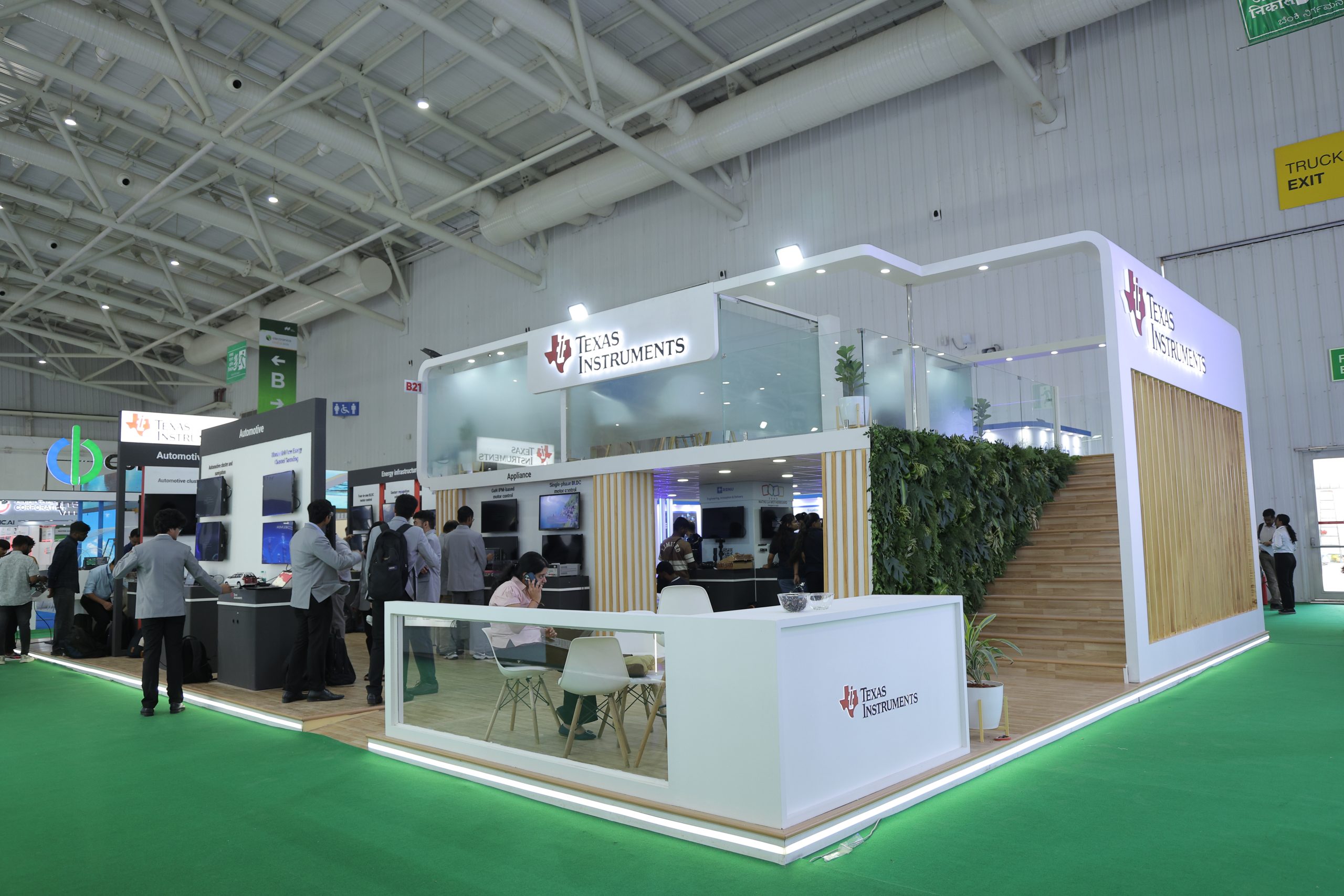
Texas Instruments (TI) is demonstrating more than 20 live demonstrations of its latest analog and embedded processing technologies at electronica India 2026, being held at the Bengaluru International Exhibition Centre (BIEC) from September 16 18. India’s transition toward clean energy is accelerating demand for applications that require high-precision power management, sensing and processing. TI is showcasing how its semiconductor technologies can support greater efficiency and reliability across electric vehicles, industrial applications and sustainable energy systems.
As part of its efforts to strengthen customer engagement in India, TI is enabling customers in the country to purchase products directly from TI, including large-quantity orders. The company says its localized purchasing capabilities provide a more convenient and seamless buying experience. Combined with its technical and design support, the initiative reflects TI’s focus on working closely with Indian customers and helping them move from design to production more efficiently.
“As engineers inventing for engineers, TI focuses on designing and manufacturing semiconductor technologies that help our customers solve increasingly complex challenges,” said Santhosh Kumar, managing director and president, TI India. “We have been part of India’s semiconductor landscape for 40 years, and our commitment here has never been stronger. electronica India 2026 gives us the opportunity to connect directly with the engineers shaping India’s next wave of innovation, building products that are smarter, safer and more energy efficient.”
Semiconductor technologies enable smarter, safer electric mobilityWith India’s adoption of electric mobility accelerating, TI’s semiconductors are enabling engineers to address the growing complexity of electric vehicle architectures, from power management and battery performance to real-time sensing and processing.
- Smarter vehicle architecture: TI is showcasing a 3D car wireframe featuring software-defined vehicle (SDV) central compute, zone control modules, 48V wiper and a Gallium Nitride (GaN)-enabled 48V audio amplifier, along with real-time wheel-speed tracking.
- Commercial vehicle advanced driver assistance systems (ADAS): TI is demonstrating 1V3R (1x camera, 3x radar) solution capable of meeting the technical requirements of ADAS mandates that apply to commercial vehicles in India.
As India scales renewable energy and modernizes its power infrastructure, TI’s semiconductor technologies are driving greater efficiency, reliability and intelligence across applications such as solar inverters, smart-grid infrastructure, motors and appliances.
- Single phase string inverter: TI is demonstrating a GaN-based 3.6kW string inverter with a single microcontroller controlling a H-Bridge bipolar modulated DC/AC inverter and a single string photovoltaic input with maximum power point tracking. The converter is optimized for high frequency operation to minimize total solution cost and size. It achieves>96.5% efficiency at full power. The single-phase string inverter platform is intended to accelerate the development of residential solar power systems.
- Meshed network architecture: TI is showcasing a Wirepas Platform, which is a standard-based connectivity platform built for infrastructure-grade IoT deployments at massive scale. It consists of two components, Wirepas mesh connectivity and the Wirepas Network Management System, and addresses diverse geographies and use cases through a wide range of radio profiles.
TI is continuing to strengthen its commitment to the Indian market by making its products easier to access and buy locally. In addition to buying directly on TI.com in Indian rupees, TI has now expanded INR capabilities to eligible customers in India through their backlog channel. INR billing offers greater cost predictability and flexibility with better delivery terms for its customers in India.
By combining semiconductor technologies with local engineering expertise, technical support and a more convenient purchasing experience, TI is helping Indian customers design and build products for evolving automotive, energy and industrial applications.
TI at electronica India 2026At electronica India 2026, in Hall 5, Booth B21, BIEC, TI will demonstrate how innovation across its analog and embedded processing portfolios is enabling what’s next in electric mobility and sustainable energy, with engineers on-site to discuss how TI’s solutions can address the challenges facing Indian engineers.
The post Texas Instruments Showcases EV and Sustainable Energy Semiconductor Innovations at electronica India 2026 appeared first on ELE Times.
Some of my planning sketches for my first projects
 | Diagram of circuit and perfboard arrangement. Mainly posted since a few people stated that my perfboard arrangement was too cramped and "couldn't work" [link] [comments] |
First connectorized micro-LED optical interconnect.
Automatic Soldering Fume Extractor with Dust and VOC Sensors
A soldering fume extractor that turns itself on when the air gets dirty. That is what Curious Scientist built using an ESP32-C3 Super Mini, a dust sensor and a VOC sensor. The device adjusts the fan speed according to the pollution level it detects and shuts off after 3 minutes with no readings. So you no longer have to remember to switch the extractor on before picking up the soldering iron.
The heart of the circuit is a compact board, the same family many makers use in IoT projects. Next to it works an Arduino Nano, which handles the reading and control side. On the panel there is room for a 1.3″ OLED display with an SSH1106 driver, managed by a compatible Arduino library. The display shows the system status and the countdown before shutdown.
Two sensors and an adaptive baselinePollution detection happens in two stages. The first is based on readings from the dust sensor, the second on those from the VOC sensor. The VOC sensor does not use the raw TVOC value directly: instead it adopts a baseline that adapts slowly and looks for significant increases relative to it. This way the system is not fooled by the small fluctuations typical of these sensors.
The GP2Y1010AU0F dust sensor works with an infrared LED briefly switched on by the microcontroller. Light scattered by the particles is picked up by a photodiode, and the output signal is proportional to the amount of dust. The minimum activation threshold for the dust parameter is 40 ug/m3. For the ENS160 sensor, the AQI value it provides ranges from 1 to 5.
The controller does not trigger on a single event or on crossing a threshold. It takes several over-threshold readings within a fixed number of readings. In practice:
- LOW level: 3 over-threshold readings out of 5
- MED level: 12 over-threshold readings out of 20
- HIGH level: 15 over-threshold readings out of 25
This logic prevents false starts. The controller starts quickly at LOW speed and increases the fan speed only if the pollution persists long enough to show that the lower speed is not enough. So the fan steps up only when it is really needed.
5 V fan and shutdown after 180 secondsThe fan is a 12 V unit, but it is powered at 5 V at a very reduced speed. This is to draw air through the device so the sensors are properly exposed and false readings are avoided. If no pollution is detected for more than 3 minutes, the extractor is switched off. The device remembers the last pollution event and counts down from there.
During the last 30 seconds of the 3-minute countdown a warning message appears. Pressing the button within those 30 seconds resets the timer. So if you are about to do another soldering job you do not have to wait for the fan to stop and start again. The countdown for the automatic fan shutdown is 180 s.
Anyone who wants to rebuild the project will find the full account of the work on the Curious Scientist website. The firmware runs on a board from the ESP32-C3 family, so it is programmed with the Arduino IDE and the usual libraries. For the OLED display you need an Arduino library compatible with the SSH1106 driver.
Replicating the project takes only a few parts: an ESP32-C3 SuperMini development board, an Arduino Nano, a dust sensor, a VOC sensor, a 1.3″ OLED display and a 12 V fan. The dust sensor is the same model used in the project, the GP2Y1010AU0F from Sharp, designed to detect dust particles. For those who want to dig deeper, maker Curious Scientist’s site collects the work on this extractor.
Source: https://curiousscientist.tech/blog/automated-fume-extractor-soldering-made-easier
Related productsThe post Automatic Soldering Fume Extractor with Dust and VOC Sensors appeared first on Open Electronics.
Web shape editor for an 8×8 WS2812B LED matrix with ESP32
Drawing a shape pixel by pixel in the browser and watching it light up on an 8×8 WS2812B LED matrix: that is what Rui Santos’ project does. The ESP32 connects to the Wi-Fi network and serves a web page with an 8×8 grid, where you pick the colour of each of the 64 RGB LEDs. Saved shapes stay in memory even after a reboot, so they can be shown on the physical matrix, reloaded into the editor or played back in sequence as a slideshow. All of it combines an asynchronous web server, a filesystem and the FastLED library on a single board.
How the web editor served by the ESP32 worksThe web page shows an 8×8 grid and for each pixel you choose the colour. A slider sets the overall brightness of the shape, which is scaled before it reaches the physical LEDs. In the code the default brightness is 128 on a scale from 0 to 255. The matrix is also driven by a single digital pin, GPIO 2, through the FastLED library, with configuration parameters for orientation, horizontal and vertical flip and colour order.
The web server is asynchronous, so the ESP32 keeps serving the page without blocking everything else. That means you can draw while the matrix stays lit on the last shape sent. Anyone who wants to rebuild the project will find the full account of the work, from the sketches to the assembly, on maker Rui Santos’ site.
Shapes saved in LittleFS and the slideshowUp to 10 shapes are saved in LittleFS as JSON, so they remain stored even after a reboot. The gallery shows a preview of every saved shape. Clicking it displays the shape on the physical matrix and reloads it into the editor for modification. You can also delete a shape, an operation that also turns off the physical LEDs, and enable a slideshow that cycles through all saved shapes with an adjustable interval. The default slideshow interval is 2000 ms between one shape and the next.
- ESP32 board
- 8×8 matrix with 64 WS2812B LEDs
- 5V 2A AC-DC power supply
- Jumper wires
- Arduino IDE with FastLED, ESPAsyncWebServer, AsyncTCP and ArduinoJSON 7.X
The software side relies on Daniel Garcia’s FastLED library, ESP32Async’s ESPAsyncWebServer and AsyncTCP, Benoit Blanchon’s ArduinoJSON 7.X and LittleFS. For anyone who wants to start from a larger matrix, the catalogue has the 16×16 flexible WS2812B Neopixel LED panel, with 256 LEDs instead of the 64 of this project.
Power and consumption of the 8×8 matrixThe WS2812B matrix is made up of 64 RGB LEDs arranged in an 8×8 grid and must be powered at 5V. At 5V each LED draws about 50mA at maximum brightness. Consequently, at full brightness in white, every 30 LEDs the matrix can draw up to 1.5A. The recommended power supply for the matrix is a 5V 2A AC-DC adapter, so with a useful margin above the current peak.
Those who prefer a shape other than the square one can look at the 8×32 addressable RGB LED matrix with 256 WS2812B LEDs, which uses the same type of LED but in an elongated geometry. The wiring stays simple: a single data wire to GPIO 2 and 5V power.
Source: https://randomnerdtutorials.com/esp32-8×8-matrix-shape-editor-web-server/
Related productsThe post Web shape editor for an 8×8 WS2812B LED matrix with ESP32 appeared first on Open Electronics.
Highly integrated approach to power system design in the AI era

Packaging innovation in the AI era has reached the doorsteps of power electronics. A new architecture uses the silicon wafer itself as the package foundation to enable a highly integrated approach to power system design. It optimizes electrical, mechanical, and thermal design together from the outset to help designers achieve higher power density and improve system performance.
Embedded Power Platform (EPP) unveiled by onsemi claims to have reimagined the package from passive housing into an active contributor to power design performance. It enables a seamless integration and interconnection of silicon, silicon carbide (SiC), and gallium nitride (GaN) technologies within a highly integrated wafer-level architecture.

Figure 1 In EPP, heterogeneous dies are embedded in silicon and connected through wafer-level redistribution layers. Source: onsemi
“For decades, the semiconductor and the package have been treated as separate technologies,” noted Hassane El-Khoury, President and CEO of onsemi. “EPP changes that by making the silicon itself part of the system architecture.” It does that by combining advanced semiconductor technologies, manufacturing, and system-level optimization into a single power design.
The AI era is creating new infrastructure challenges that computing power alone can’t solve. Take data centers, for instance, where design engineers must move and manage more electricity in server racks while controlling heat, efficiency, cost, and development time. That limits how much compute capacity can fit within a rack.
That’s mainly because traditional power system design approaches treat power electronics, mechanical design, and thermal design as separate engineering challenges. As a result, each layer is optimized independently and sequentially, so decisions made at one stage can create compromises in another. That, in turn, leads to additional engineering iterations, costly late-stage changes, and longer development cycles.
EPP replaces the sequential model with a common platform that can be co-designed, co-simulated, and co-optimized. That transforms it into a technology-agnostic platform that supports different applications and semiconductor materials while scaling across multiple power levels. As a result, multiple devices such as FETs, drivers, and controllers can be embedded together in a single package and co-optimized for electrical, thermal, and mechanical performance.

Figure 2 EPP claims to introduce a fundamentally new approach to how power is delivered, managed, and optimized. Source: onsemi
This enables tighter electrical coupling, combines power and control in a single platform, and reduces system-level complexity. According to onsemi, in a solid-state circuit-breaker design, the EPP-based solution was approximately 50% smaller and 20% cooler than existing designs.
Beyond data center power
Carmaker Subaru—an early engagement partner for EPP—is working with onsemi to evaluate how the platform could support future electrified vehicle architectures. Subaru will gain early access to engineering samples, simulation models, and technical expertise as the two companies explore opportunities to improve vehicle performance and streamline development.
Efficiency losses, thermal limitations, development complexity, and system size often constrain EV traction inverters. Here, EPP’s scalable architecture helps develop a single inverter platform that spans low-end to high-end vehicle applications. This lets carmakers reuse a common design across multiple vehicle models and power classes, reducing R&D and manufacturing costs, accelerating qualification and development cycles, improving vehicle range, and lowering system costs.
As AI, automotive, and industrial markets drive demand for more power in less space, a new architecture claims to redefine system power delivery by integrating multiple dies into a single silicon device. EPP also claims to enable 3 – 5x higher power density than current solutions through a highly integrated approach to power system design.
These claims will surely be tested in data center and EV power designs, where designers must improve efficiency while managing heat, size, and cost. EPP is expected to begin sampling in 2026 with strategic customers and ecosystem participants across automotive and AI applications.
Related Content
- The shift to 800-VDC power architectures in AI factories
- Power systems: the first parameter to evaluate is efficiency
- Low Power Design Techniques, Design Methodology, and Tools
- LTpowerPlanner: A system-level power architecture design tool
- Designing a data center power architecture with supply and processor rail-monitoring solutions
The post Highly integrated approach to power system design in the AI era appeared first on EDN.
Hackaday Podcast: Stirling Engines, Contactless Watches, and Maker Challenges
In episode 384, the Hackaday podcast offers a curated overview of the week’s most interesting projects and news in the world of electronics and hacking. Editors Elliot Williams and Al Williams comment on their favorite articles, read listener messages in the Mailbag segment, and announce new challenges. They also showcase projects like a fully 3D-printable thermoacoustic Stirling engine, a turntable that reads MOD files optically, and a Casio F-91W watch modified for contactless payments.
Thermoacoustic Stirling engine and other projectsAmong the most fascinating projects, a thermoacoustic Stirling engine made entirely with 3D printing stands out. This type of engine uses sound waves to generate motion, and the ability to print it completely makes it accessible to many makers. The podcast also discusses a turntable that reads MOD files optically, a creative solution that bridges the digital and analog worlds. Finally, a Casio F-91W modified for contactless payments shows how modern technology can be integrated into a classic object.
The podcast is not limited to projects: it also covers the history of space stations starting from the 1800s, a fascinating journey through the milestones that led to modern orbital structures. Additionally, must-read articles are discussed, including a talk on making magical PCBs and quick tips like emulating an iPod or making an LCD interface look like classic spy gear. The project page on Hackaday.io collects the details and links to dive deeper into each topic covered.
Challenges and contests for makersThe podcast announces the Retrocomputing Challenge 2026 and Supercon 2026, two unmissable events for enthusiasts. It also reminds listeners about the One Hertz Challenge, the currently open contest that asks you to design a device in which something happens once per second.
These challenges stimulate creativity and push makers to exceed their limits. The podcast also offers practical tips for those who want to get involved, such as using a TO-220 power transistor to handle more demanding loads. For those starting with prototyping, a perfboard for Arduino is the ideal starting point. Finally, for projects that require a response to movement, a high-sensitivity vibration sensor can make a difference.
Hackaday Podcast episode 384 confirms itself as a valuable resource for those following the world of electronics. Thanks to the editors’ comments and listener submissions, it offers a complete and up-to-date view. The Mailbag segment also allows direct interaction with the community, making each episode unique and participatory.
Source: https://hackaday.io/contests
Related productsThe post Hackaday Podcast: Stirling Engines, Contactless Watches, and Maker Challenges appeared first on Open Electronics.
SFP: Add-in module delivers diminutive performance, flexibility

Want to network-connect your gear using prevalent wired Ethernet? Or interference-impervious optical fiber? How about a bandwidth boost? Or a range extension? SFP and its siblings do it all.
One recent sequential-coverage cadence of mine just wrapped up, with part 4 of the “Debugging intermittent Comcast” run done. Another, my longstanding TP-Link smart plug teardown series, is nearing the finish line, with its next entry queued up to appear on EDN a week from next Monday and its final entry scheduled for next-month publication.
But if indeed all good things must sooner or later come to an end, other good things can also emerge in their stead. That’s what I hope will be the case for the small form-factor pluggable (SFP) module teardown series set to start next Monday. I first learned of SFP through my efforts to galvanically isolate my various LAN devices from lightning EMI-prone Ethernet and coax cables running outside of my residence.
Multi-gig gains ascendancyI’ve subsequently become intrigued (also with pending editorial-coverage consequences) with the increasing (and dramatically so) cost-effectiveness of mainstream network switches, routers, and other devices based on 2.5 GbE technology. Take a look, for example, at this enterprise managed switch from the late 2000s, which cost several thousand dollars when brand new.

Granted, it has 24 primary Ethernet ports, but they “only” offer 10/100 Mbps. At far left are two more GbE Ethernet ports. And in-between the two RJ-45 arrays are two 1 Gbit SFP ports.
Fast-forward to today. This switch is admittedly unmanaged and has only eight RJ-45 ports.

But those RJ-45 ports are 2.5 GbE. The SFP ports are next-gen SFP+, 10 GbE. And the price tag? $41.39 at Amazon as I write these words.
Or this one:

Four fewer RJ-45s, albeit still 2.5 GbE. Once again, two 10 GbE SFP+ ports. And the price? $31.99. One of them is on an Amazon delivery truck headed to me later today as we speak, in fact. And in a near-future planned post, I’ll even detail how it’s possible to (and I in fact did) transform one into a fully user-managed variant using hacked factory firmware and/or open-source software.
Why 2.5 GbE (along with, to a lesser extent, 5 GbE) has become mainstream is a topic for another post another day (soon). Similarly, I’ll save for the near future more discussion on why 10 GbE SFP+ ports are appearing on mainstream gear like this. Today, in advance of a plethora of teardowns to come on a diversity of module variants I’ve been collecting in recent weeks, I just want to focus on what SFP is, along with its predecessor and siblings.
Without further ado, and focusing predominantly on the “flavors” most commonly used in consumer and workgroup settings, therefore in highest production volume, which typically translates to lowest cost (if you feel like your head’s about to explode after absorbing the full suite of SFP implementation options documented on Wikipedia, it’s perfectly understandable!)…
Mechanical form factors
Before SFP, there was GBIC, the gigabit interface converter, initially defined in 1995 and used with Gigabit Ethernet and Fibre Channel. As Wikipedia notes, “By standardizing on a hot swappable electrical interface, a single gigabit port can support a wide range of physical media, from copper to long-wave single-mode optical fiber, at lengths of hundreds of kilometers.”

Keeping in mind inevitable bandwidth extrapolation, thanks to further technology evolution, the same basic definition applies to 20-pin SFP, therefore explaining its alternative name, mini-GBIC.


Quad SFP (QSFP), as the name implies, supports four simultaneous bidirectional data lanes (therefore the 38-pin connector). The first picture above is of a standalone transceiver; the second shows an active optical cable (AOC) version conceptually like, albeit of course more complex than, the SFP-based ones I’m currently using in my network for galvanic isolation purposes.
The module is of the same height (8.5 mm/0.33 in.) as SFP, as is the XFP module I’ll discuss next. But it’s wider than SFP (18.35 mm/0.722 in. vs 13.4 mm/0.53 in.), although adapters can allow SFP modules to fit in QSFP sockets. And it’s also deeper than SFP; 72.4 mm/2.85 in. vs 56.5 mm/2.22 in.

Last, and least common nowadays, is another SFP precursor, aforementioned 30-pin XFP, dating from 2002. It’s even deeper than QSFP, 78.0 mm/3.07 in. The above photo is of it alongside SFP.
System interfaces
Commonplace SFP interfaces run at 100 Mbps and 1, 2.5 and 5 Gbps. The bitrate similarly to Ethernet counterparts is not accidental  SFP+ leverages the same SFP mechanical form factor discussed earlier but runs at 10 Gbps and 25 Gbps, the latter alternatively known as SFP28. Less common 50 and 100 Mbps SFFP+ variants (SFP56 and SFP112) are also available, as are “DD” double density flavors which leverage up to 8 data lanes. Higher speed SFP+ versions migrate from non-return-to-zero (NRZ) modulation to four-level pulse-amplitude modulation (PAM-4).

SFP modules connect to each other, as well as directly to system in some cases, via three main cable material and associated transceiver options: fiber optics in conjunction with electro-optical converters, RJ-45 Ethernet, and basic copper wire.
I’ll discuss fiber optics in more detail in the next section; for now, I’ll note the following:
- Both plastic and glass cable construction material options are available. Plastic characteristics include (with glass characteristics essentially the exact opposite):
- Lower cost
- Greater flexibility and overall handling safety
- But much shorter usable distance due to high attenuation loss
- Low tolerance of temperature extremes
- When the cable is permanently installed to SFP modules on both ends, it’s referred to (as alluded to earlier) as an active optical cable (AOC).
RJ-45 modules mate the SFP or SFP+ circuitry to an Ethernet transceiver. Speeds up to 10 GbE, such as with the module shown at the top of this section, are widely available. These modules tend to run “hotter” than fiber optical or basic wire alternatives, all other factors being equal.
Passive direct-attached-cable (DAC) wire harness-based cables are the most elementary version of this particular form factor, with the shortest effective range. Active copper cables (ACC), as a helpful white paper from NADDOD explains, “use a redriver chip architecture, employing continuous time linear equalization (CTLE) to boost signals on the receiver (Rx) side, acting as analog signal amplifiers.” And active electrical cables (AECs) “are more advanced, using a retimer chip architecture to amplify and equalize signals at both transmitter (Tx) and receiver (Rx) ends, with added clock data recovery (CDR) to reduce jitter, offering higher signal integrity and clearer data transmission.”
Wavelengths
SFP modules most commonly run at the following wavelengths (all are center frequencies):
- 850 nm (“multimode”)
- 1300 nm (“multimode”)/1310 nm (“single-mode”)
- 1550 nm (“single-mode”)
The distinction between multimode and single-mode fiber optics is important to comprehend and keep in mind, as the two technologies are not interchangeable (although some modules will work with both associated cable material types).
Multimode was historically much less expensive to implement, at the tradeoff of lower usable transmission distance. It features a comparatively larger cable core (50 to 62.5 microns) that lets multiple light signals travel down different paths at the same time, and it usually uses lower-cost LEDs or vertical-cavity surface-emitting lasers (VCSELs).
Single-mode features a comparatively tiny core (about 8 to 10 microns), which allows only a single ray of light to pass straight through without bouncing off the edges, and it uses focused lasers as a light source. Its historical cost disadvantage versus “multimode” has more recently decreased, due in part to the availability of non-proprietary, widely compatible modules. And as noted earlier, it generally specifies much longer usable transmission distances.
Cable tiers
We’ve already discussed fiber optic cable materials and construction options, along with associated light source and reception approaches. Each combination also has multiple quality tiers, which are commonly color-coded for ease of user recognition and interpretation.
Multimode cable comes in OM1 through OM5 options, with OM1 and OM2 now in legacy status and OM3 and OM4 most common nowadays. The fundamental tradeoffs between them involve lower cost (OM3) versus higher modal bandwidth and longer transmission spans (OM4).
For single-mode fiber optics, it’s simpler—OS1 and OS2—although the two types are incompatible in that they cannot be directly connected to each other. Cost, bandwidth and transmission distance are again the predominant evaluation criteria between them, although construction variances also tend to favor OS1 for indoor use and OS2 for outdoor applications.
Fiber connectors
Legacy GBIC deployments used the Standard (or Subscriber) Connector (SC) to mate cables to modules. Newer SFP-based implementations have switched to the much smaller Lucent Connector (LC). AOC fiber interconnect with SC plugs on one end and LC plugs on the other is also commonly available to bridge legacy and newer networking hardware.
Module flavors
As mentioned earlier, I’ve got a bunch of modules in hand, which I plan to tear down and internals-share with you in the coming months. As you can likely already imagine, the implementation diversity inherent in combining the numerous technology variables discussed in the previous sections results in oft-“interesting” module results. Here’s what I’ll be dissecting:
- 1 Gbit SR (short range, multimode) SFP module
- 1 Gbit LX (long range, usable with both single-mode and multimode cable at differing distances) SFP+ module
- 1 Gbit SFP to RJ45 transceiver module
- 5 Gbit ZX+ (extended long-haul range, single-mode) SFP module
- 10 Gbit IR (intermediate range, single-mode) SFP+ module
- 10 Gbit 0.3 meter/1 foot DAC cable
- 25 Gbit SR (short range, multimode) SFP+ (SFP28) module
- 40 Gbit SR QSFP+ module
The last one, whose image is at the top of this section, is particularly interesting (at least to me). It’s a 1 Gbit “BX” SFP module, with BX standing for bidirectional. Compared to the prior fiber-based modules, which use one strand for transmission and the other for reception (so you need to be sure when you hook them up that each strand’s transmission connection on one module end mates up with the other module’s receiver connection at the other end, and vice versa!), a BX module both transmits and receives across a common single cable strand.
The wavelengths employed by each module are vendor-specific, so you need to be careful in reading the specifications to ensure that you’ll end up with a transmit-and-receive wavelength matched pairing on both ends of the cable. Or just play it safe and buy all your modules from a single supplier, using a common model number.
And here’s a further “wrinkle” on the concept; in the above picture, since only a single strand is in use, there’s only one exposed optical connector site necessary. cSFP modules instead continue to use both fiber cable connectors, combining two bidirectional electro-optical subsystems in one module for doubled per-cable transfer rates. Tricky, eh?
That’s all I’ve got for you today. Look for my initial module teardown in the series, of the aforementioned 10 Gbit LX SFP+ module, to come early next week. And until then, I as always welcome your series-so-far thoughts in the comments!
—Brian Dipert is the associate editor, as well as a contributing editor, at EDN.
Related Content
- TP-Link MC220L: Media conversion keeps the network well
- The whole-house LAN: Achilles-heel alternatives, tradeoffs, and plans
- Design considerations in high-speed fiber networks
The post SFP: Add-in module delivers diminutive performance, flexibility appeared first on EDN.
🎥 Відкритий діалог КПІшників зі Стівеном Голдфарбом

⚛️ Сучасна фізика, експериментальні дослідження й фундаментальна наука: відкритий діалог КПІшників зі Стівеном Голдфарбом — франко-американським фізиком-експериментатором у галузі фізики елементарних частинок.
ROHM’s silicon carbide used in electric powertrain of BMW’s ‘Neue Klasse’ Gen 6 EVs
An i386 PC on the Raspberry Pi Pico 2: Tiny386 Emulator Runs on RP2350
A development board costing a few euros can become a complete i386 PC. That is what the Tiny386 emulator, ported to RP2350 boards by Mikhail Matveev, achieves: the Raspberry Pi Pico 2 emulates an i386 CPU, talks to an SD card, drives a VGA or HDMI output and accepts keyboard, mouse and gamepad. The firmware boots DOS, Windows 3.x, Windows 95 and Linux, so it behaves like a real Nineties PC, only much smaller.
At its heart is Chunhui He’s Tiny386 core, which emulates a complete i386 CPU with partial i486 and i586 instructions and an optional x87 FPU. The integration on the RP2350 platform is called Pico-286 and borrows the hardware patterns of QuakeGeneric. The PC peripherals code comes from QEMU, while the BIOS is SeaBIOS with its VGA BIOS. Everything runs on Raspberry Pi Pico SDK version 2.0 or later.
8MB PSRAM, SPI SD and a 378 MHz clockMemory is the main constraint for an x86 emulator on a microcontroller, and here it is solved with the 8MB PSRAM mounted on the board. The emulator uses up to 8MB of RAM, while the settings menu lets you configure from 1 to 8 MB. The default CPU frequency in the build is 378 MHz, with a 504 MHz option, and the PSRAM runs at 133 MHz with a 166 MHz option. These are numbers to keep an eye on, because pushing the clock helps emulation but runs hotter and draws more power.
Storage goes through the SD card in SPI mode, managed by the FatFs module for the FAT filesystem. Disk images are read at runtime through a disk manager opened with Win+F12: from there you choose floppy, hard disk and CD-ROM. The maximum supported hard disk image size is 2GB, while standard floppies are 1.44MB, that is 1474560 bytes. The settings menu, on the other hand, opens with Win+F11 and changes the emulator configuration on the fly, without rebooting.
VGA or HDMI, PS/2, USB Host and I2S audioVideo output comes on a VGA or HDMI connector and covers text and graphics modes up to 640×480. For input there are two routes. The first is classic PS/2, with dedicated keyboard and mouse. The second uses the RP2350’s native USB Host, so USB keyboards and mice can be connected. On top of that there is support for the NES gamepad, which can work in mouse emulation mode. Audio comes out of an I2S DAC and the FM synthesis for AdLib comes from the MAME FM Sound Generator, the fmopl module.
- Raspberry Pi Pico 2 with RP2350 as the base board
- 8MB PSRAM to reach 8MB of emulated RAM
- SD card in SPI mode for floppy, hard disk and CD-ROM
- PS/2 keyboard and mouse, or USB keyboard and mouse via native USB Host
- NES or SNES gamepad with mouse emulation mode
- I2S DAC for audio output
- VGA or HDMI connector for video
Anyone who wants to rebuild the project will find the code to compile in Mikhail Matveev’s repository, with the Pico-286 integration for RP2350 and the third-party modules already wired in. The INI file parser is inih, the filesystem is FatFs, and the BIOS and VGA BIOS must be supplied as bios.bin and vgabios.bin. The build is done with Raspberry Pi Pico SDK 2.0 or later, so you need an up-to-date ARM toolchain and a bit of patience with clock configuration.
Assembly does not require exotic components: the board, the PSRAM, the SD slot, the connectors and the DAC. For the storage side, a MicroSD Card Reader module with SPI interface replicates the SPI read scheme used by the firmware for floppy, hard disk and CD-ROM. For audio output, a DAC audio converter with I2S interface covers the same function as the DAC described in the project.
The result is an i386 PC with complete peripherals at the cost of an inexpensive development board. DOS, Windows 3.x, Windows 95 and Linux run on pocket-sized hardware, with 8MB of RAM, 640×480 graphics and SD storage. For anyone who wants to understand how an x86 machine is emulated on a microcontroller, or simply wants a portable bench DOS machine, this is a concrete starting point.
Source: https://github.com/rh1tech/frank-386
Related productsThe post An i386 PC on the Raspberry Pi Pico 2: Tiny386 Emulator Runs on RP2350 appeared first on Open Electronics.
Koode Bot: Offline Hospital Triage with Edge AI on Raspberry Pi 5
Koode Bot is a hospital reception system that works without internet. An AI-powered kiosk interviews patients in Malayalam, assigns a department, and generates a clinical summary for the doctor. An ESP32 robot then physically escorts the patient to the department. The project is designed to respect privacy and reduce staff workload.
The core of the system is a Raspberry Pi 5 with 8 GB of RAM. The patient selects a language on the touchscreen—Malayalam, Hindi, or English—and speaks into a USB microphone. The audio is converted to text by faster-whisper and sent to the Gemma 4 E2B model running on Ollama. The model conducts a structured clinical interview, asking follow-up questions based on reported symptoms.
Data flow and clinical report generationAt the end of the interview, the model generates a clinical report in JSON with department, urgency, and summary. The report is saved in SQLite. The kiosk displays the token and assigned department, and sends an MQTT message on the topic koode/bot/navigate. The token has the format K0419001: the initial K, month and day, and a daily counter.
Report generation takes 60–120 seconds. The system handles up to 12 question-and-answer exchanges in the interview. Model response latency is 10–30 seconds, while speech recognition takes 2–6 seconds. Model loading time is about 35 seconds. RAM usage is about 9 GB.
The Koode Bot robot and ultrasonic navigationThe Koode Bot robot uses an ESP32-S3 and receives the MQTT message with the assigned department. MQTT latency is 1 second. The robot escorts the patient using ultrasonic sensors for navigation. An HC-SR04 sensor detects obstacles, while an L298 driver controls the 12 V DC motors.
The department misclassification rate is about 15%. The system has significant potential for epidemic detection by analyzing symptoms collected from interviews. Additionally, the offline nature protects sensitive patient data.
The project is documented in the shan repository. Those who want to replicate it will find code for the Raspberry Pi and the ESP32, plus the configuration for Ollama and the models.
What you need to rebuild the projectThe main components include a Raspberry Pi 5, an official touchscreen, a USB microphone, and a Hailo-8 AI HAT accelerator. For the robot, you need an ESP32-S3, an HC-SR04 ultrasonic sensor, an L298 driver, and 12 V DC motors.
The software runs on Ollama with the Gemma 4 E2B model (Q4_K_M). The backend uses Flask, SQLite, and MQTT (mosquitto). On the robot, PubSubClient and ArduinoJson handle communication. For those starting from scratch, the Raspberry Pi 5 is the recommended base for the kiosk.
- Raspberry Pi 5 with 8 GB of RAM
- Raspberry Pi Touch Display
- USB microphone
- Hailo-8 AI HAT
- DFRobot FireBeetle ESP32 IOT Microcontroller
- HC-SR04 ultrasonic sensor
- L298 motor driver
- 12 V DC motors
The system is designed for hospitals with reduced staff or areas with limited connectivity. Privacy is guaranteed by the fact that no data leaves the device. The project demonstrates how edge AI can bring intelligence to critical contexts without depending on the cloud.
Source: https://github.com/lil-shan/Koode
The post Koode Bot: Offline Hospital Triage with Edge AI on Raspberry Pi 5 appeared first on Open Electronics.
Some of my first perfboard projects
 | From left to right, oldest(first) to newest, an LED light dimmer, a charge pump, a light blinker, and a monostable ne555 for extending the length of a pulse from a motion sensor [link] [comments] |
Sensor sharpens infrared in-cabin imaging

The ST SafeSense VD56GA 1.1-Mpixel automotive image sensor enables infrared in-cabin sensing for driver and occupant monitoring applications. Based on ST’s DeepNIR BSI pixel architecture, the sensor delivers 35% higher modulation transfer function (MTF) and nearly 60% higher quantum efficiency (QE) than the previous generation. The higher MTF and infrared sensitivity result in sharper images, while the sensor’s small CSP allows discreet in-cabin camera designs for space-constrained installations.

With 2.43×2.43-µm pixels, the global-shutter sensor’s 1.1-Mpixel architecture achieves virtual 2-Mpixel performance. According to ST, the VDA56GA can reduce overall camera-module costs through lower-cost optics, simplified infrared illumination, and less demanding optical filtering. Embedded image-processing functions, including mirror, crop, dark calibration, auto exposure, and piecewise-linear processing, eliminate the need for external image processing. Together, these features can help designers deploy driver and occupant monitoring across a broader range of vehicle models.
The sensor is undergoing AEC-Q100 Grade 2 qualification, with a −40°C to +125°C operating junction-temperature range. It is compliant with ISO 26262 for ASIL B system integration and ISO/SAE 21434 for automotive cybersecurity.
Samples are available now. Pricing information and sample requests are available from local ST sales offices.
The post Sensor sharpens infrared in-cabin imaging appeared first on EDN.
Transient voltage suppression devices reach 11 kW with flat clamping

Vishay’s XFD11KxxCA flat-clamping transient voltage suppression (TVS) devices provide 11 kW of peak pulse power dissipation at 10/1000 µs. Offered in surface-mount DO-218AC packages, the bidirectional devices maintain a low clamping ratio (VC/VBR) close to 1.0, supporting high power density.

The XFD11KxxCA series comprises 15 devices, each available in commercial and AEC-Q101 qualified grades. They have clamping voltages of 40.6 V to 104.0 V, breakdown voltages from 36.7 V to 104 V, and standoff voltages from 33 V to 85 V, making them suitable for 12-V, 24-V, and 48-V automotive powertrains. At the same standoff voltage, they have lower clamping voltage than conventional TVS products in DO-218 packages and deliver approximately 1.6 times higher peak pulse current, up to 207.1 A at 10/1000 µs.
Additional key specifications include an 8/20-µs surge capability of up to 2140 A and maximum leakage current of 10 µA at the standoff voltage (VWM) to minimize power loss. The series’ low, stable clamping and breakdown voltages over a wide temperature range of -55°C to +175°C allow the use of lower-voltage downstream components, reducing voltage overshoot and enabling smaller design guard bands.
Samples and production quantities of the XFD11KxxCA series are available now, with lead times of 12 weeks.
The post Transient voltage suppression devices reach 11 kW with flat clamping appeared first on EDN.
SPAD sensor processes photon events on-chip

Singular Photonics’ Litavis is a CMOS single-photon avalanche diode (SPAD) image sensor with integrated digital photon processing on-chip and in-pixel. By processing photon events directly on-chip, it reduces the volume of raw data that must be transferred and processed externally. According to the company, Litavis enables scalable real-time imaging systems with lower latency and improved power efficiency.

The 3D-stacked, back-side-illuminated (BSI) sensor captures spatial and temporal information while extracting scene information such as depth and event characteristics. Its software-configurable architecture combines photon-counting imaging, programmable time gating, and photon timing within a scalable SPAD array. Litavis supports intensity, timing, and histogramming modes concurrently, allowing users to dynamically adjust sensor parameters in software without requiring a new hardware design.
Litavis provides continuous 256×256-pixel photon-counting imaging under low-light conditions and simultaneously generates time-stamped photon events across a 64×64-macropixel timing grid. It delivers 47% photon detection efficiency (PDE) at 785 nm, 37-ps timing resolution, and 4.3-ns dead time, with a 100% fill factor enabled by microlenses.
The SPAD-based sensor targets applications including machine vision, physical AI, robotics, depth sensing, and scientific imaging. A timeline for sensor availability was not provided at the time of this announcement.
The post SPAD sensor processes photon events on-chip appeared first on EDN.
Anti-surge resistors reduce component count

Anti-surge chip resistors in Rohm’s SDR01 series deliver a rated power of 0.33 W in the 0402 (1005 metric) package. The devices save board space and lower component count by replacing larger-size resistors in automotive, industrial, and AI server applications that require increased mounting density.

With optimized resistive element and electrode designs, the SDR01 series achieves a high rated power in the 0402 size while maintaining the reliability expected of high anti-surge chip resistors. The devices maintain their 0.33-W rating at terminal temperatures up to 125°C, making them suitable for demanding thermal environments.
Qualified to AEC-Q200, the chip resistors operate over a temperature range of -55°C to +155°C. The SDR01MZPF has a resistance tolerance of ±1% and a resistance range of 1 Ω to 2.2 MΩ, with a TCR of ±100 ppm/°C from 10 Ω to 2.2 MΩ. The corresponding ratings for the SDR01MZPJ are ±5%, 1 Ω to 10 MΩ, and a TCR of ±200 ppm/°C from 10 Ω to 10 MΩ, respectively.
The SDR01 series is now in mass production.
The post Anti-surge resistors reduce component count appeared first on EDN.
Pages



