
Feed aggregator
Týr-the-Pruner: Search-based Global Structural Pruning for LLMs
Courtesy: AMD
Key Takeaways:
- End-to-end global structural pruning: Týr-the-Pruner jointly optimises pruning and layer-wise sparsity allocation, avoiding two-stage global ranking pipelines.
- Multi-sparsity supernet with expectation-aware error modelling: Layers are pruned at multiple sparsity levels and evaluated collectively to capture cross-layer dependencies.
- Coarse-to-fine evolutionary search under a fixed sparsity budget: Sparsity-shift mutations preserve global constraints while progressively refining resolution (12.5% → 1.56%).
- Taylor-informed, backprop-free local pruning: First- and second-order saliency guides structured pruning with minimal functional drift.
- Near-dense accuracy with real hardware gains: Up to 50% parameter reduction retains ~97% accuracy on Llama-3.1-70B, accelerating inference on AMD Instinct GPUs.
As large language models (LLMs) scale into the tens and hundreds of billions of parameters, pruning has re-emerged as a critical lever for improving inference efficiency without sacrificing accuracy. AMD’s Týr-the-Pruner advances this frontier with a search-based, end-to-end framework for global structural pruning, delivering up to 50% parameter reduction while retaining ~97% of dense accuracy on Llama-3.1-70B—a new state of the art among structured pruning methods.
Accepted to NeurIPS 2025, the work also demonstrates tangible inference speedups on AMD Instinct GPUs, reinforcing pruning’s relevance not just as a compression technique, but as a practical path to deployment-scale efficiency.
Why global sparsity matters
Local structural pruning is appealing for its simplicity and efficiency: layers are pruned independently, often allowing even hundred-billion-parameter models to fit on a single device. However, this approach enforces uniform per-layer sparsity, overlooking how errors and redundancies propagate across layers.
Existing “global” pruning methods attempt to address this by first ranking substructures across layers and then pruning accordingly. While intuitive, this two-stage pipeline breaks end-to-end optimisation and struggles to capture inter-layer interactions.
Týr-the-Pruner flips the paradigm. Instead of ranking structures before pruning, it first constructs a multi-sparsity supernet and then searches directly for the optimal layer-wise sparsity distribution under a fixed global budget—yielding a truly end-to-end global pruning strategy.
Inside Týr-the-Pruner: How It Works
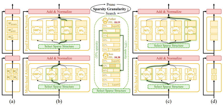
Figure 1. An overview of Týr-the-Pruner. Large language models (a) will be effectively locally pruned across multiple sparsity ratios and constructed into a supernet (b). An iterative prune-and-search strategy will be used to select the optimal sparse structure for each layer while maintaining a target overall sparsity ratio: pruning and sparsity-shift-driven evolutionary search are implemented iteratively with a coarse-to-fine sparsity interval granularity (c). Ultimately, the post-pruned LLM with the optimal sparsity distribution (d) is obtained.
Building a Reliable Supernet
The process begins by locally pruning every layer across multiple sparsity levels. Týr employs Taylor-informed saliency (first- and second-order) alongside backprop-free weight adjustment, applied progressively to minimise performance perturbations.
To ensure that different pruned variants remain mutually consistent, the framework introduces expectation-aware error accumulation, addressing the otherwise ambiguous error propagation that arises when multiple pruned copies coexist within a supernet.
Coarse-to-Fine Global Search
Once the supernet is established, Týr performs an evolutionary sparsity-shift search. Each mutation preserves the global sparsity budget—for example, making one layer slightly denser while another becomes equivalently sparser. Candidate models are evaluated using distillation-based similarity metrics over hidden activations and logits.
A naïve fine-grained search would be intractable: for an 80-sublayer model, even modest sparsity resolution would imply an astronomically large configuration space. Týr sidesteps this with an iterative coarse-to-fine strategy:
- The search begins with a coarse sparsity interval (12.5%) and just nine candidates per layer.
- After identifying a strong sparsity pattern, the search recentres and halves the interval (12.5% → 6.25% → 3.13% → 1.56%).
- After four iterations, Týr reaches fine-grained sparsity resolution while keeping each iteration’s effective search space manageable.
This design steadily narrows the search, accelerates convergence, and efficiently uncovers the optimal global sparsity distribution.
Results: Accuracy and efficiency on AMD hardware
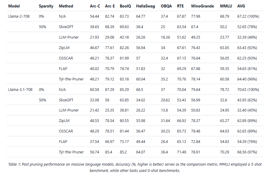
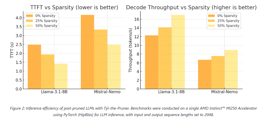
Across models and benchmarks, Týr-the-Pruner consistently preserves near-dense accuracy while delivering meaningful efficiency gains on AMD Instinct MI250 accelerators.
At 50% sparsity, the method retains 96–97% average accuracy on 70B-scale models—outperforming structured pruning approaches such as SliceGPT, LLM-Pruner, and FLAP. On smaller models, the runtime benefits are equally compelling: for Llama-3.1-8B and Mistral-Nemo, pruning cuts time-to-first-token by up to 1.75× and boosts decode throughput by up to 1.38×.
These results position pruning as a first-class optimisation technique for large-scale LLM inference, particularly on modern accelerator architectures.
Practical Considerations: Memory and Search Efficiency
While supernets can be large, Týr keeps memory usage close to that of a single dense model by storing pruned substructures on disk and loading only the active subnet into high-bandwidth memory. Disk footprints remain manageable—around 40 GB for 7–8B models and ~415 GB for 70B models—with older artefacts cleaned up between iterations.
The evolutionary search itself is computationally efficient. Evaluations proceed under progressively increasing token budgets (2K → 16K → 128K), converging rapidly thanks to the coarse-to-fine schedule. For 8B-scale models, a single search iteration completes in a few hours, keeping overall runtime well within practical limits.
Summary
Týr-the-Pruner represents a shift in how global structural pruning is approached. By unifying pruning and sparsity allocation into a single, end-to-end search process—and combining it with expectation-aware error modelling and coarse-to-fine optimisation—the framework achieves both high accuracy retention and real-world inference acceleration.
With up to 50% parameter reduction and ~97% accuracy preserved on Llama-3.1-70B, Týr-the-Pruner demonstrates that global pruning can be both principled and practical—setting a new benchmark for structured pruning in the era of large-scale LLM deployment.
The post Týr-the-Pruner: Search-based Global Structural Pruning for LLMs appeared first on ELE Times.
LEDS Manufactured Backwards
 | My college Electronics class final was to simply solder on parts of a pre-made circuit, and in my case it was an LED Christmas Tree. After soldering 36 TINY AS HELL LEDS, I tested it and there was no lights turning on…. Decided to test an extra LED and turns out the legs were manufactured with the long leg as the negative side and the short leg as the positive side. I’m so cooked [link] [comments] |
Wolfspeed produces single-crystal 300mm silicon carbide wafer
Altum RF renews ISO 9001:2015 certification
📱Конференція трудового колективу КПІ ім. Ігоря Сікорського
26 січня 2026 року відбудеться конференція трудового колективу КПІ ім. Ігоря Сікорського у залі засідань Вченої ради.
5 octave linear(ish)-in-pitch power VCO

A few months back, frequent DI contributor Nick Cornford showed us some clever circuits using the TDA7052A audio amplifier as a power oscillator. His designs also demonstrate the utility of the 7052’s nifty DC antilog gain control input:
- Power amplifiers that oscillate—deliberately. Part 1: A simple start.
- Power amplifiers that oscillate—deliberately. Part 2: A crafty conclusion.
Eventually, the temptation to have a go at using this tricky chip in a (sort of) similar venue became irresistible. So here it is. See Figure 1.
 Figure 1 A2 feedback and TDA7052A’s antilog Vc gain control create a ~300-mW, 5-octave linear-in-pitch VCO. More or less…
The 5-V square wave from comparator A2 is AC-coupled by C1 and integrated by R1C2 to produce an (approximate) triangular waveshape on U1 pin 2. This is boosted by A1 by a gain factor of 0dB to 30dB (1 to 32) according to the Vcon gain control input to become complementary speaker drive signals on pins 5 and 8.
A2 compares the speaker signals to its own 5-V square wave to complete the oscillation-driven feedback loop thusly. Its 5-V square wave is summed with the inverted -1.7-Vpp U1 pin 8 signal, divided by 2 by the R2R3 divider, then compared to the noninverted +1.7-Vpp U1 pin 5 signal. The result is to force A2 to toggle at the peaks of the tri-wave when the tri-wave’s amplitude just touches 1.7 Vpp. This causes the triangle to promptly reverse direction. The action is sketched in Figure 2.

Figure 2 The signal at the A2+ (red) and A2- (green) inputs.
This results in (fairly) accurate regulation of the tri-wave’s amplitude at a constant 1.7 Vpp. But how does that allow Vcon to control oscillation frequency?
Here’s how.
The slope of the tri-wave on A1’s input pin 2 is fixed at 2.5v/(R1C2), or 340 v/s. Therefore, the slopes of the tri-waves on A1 output pins 5 and 8 equal ±U1gain*340 v/s. This means the time required for those tri-waves to ramp through each 1.7-V half-cycle = 1.7/(U1gain*340v/s) = 5ms/U1gain.
Thus, the full cycle time = 2*(5ms/U1gain) = 10ms/U1gain, making Fosc = 100Hz*A1gain.
A1 gain is controlled by the 0- to 2-V Vc input. The Vc input is internally biased to 1 V with a 14-kΩ equivalent impedance as illustrated in Figure 3.

Figure 3 R4 works with the 14 kΩ internal Vc bias to make a 5:1 voltage divider, converting 0 to 2 V into 1±0.2 V.
R4 works into this, making a 5:1 voltage division that converts the 0 to 2 V suggested Vc excursion to the 0.8 to 1.2 V range at pin 4. Figure 4 shows the 0dB to 30dB gain range this translates into.

Figure 4 Vc’s 0 to 2 V antilog gain control span programs A1 pin 4 from 0.8 V to 1.2 V for 1x to 32x gain and Fosc = 100HzA1gain = 100Hz(5.66Vc) = 100 to 3200Hz
The resulting balanced tri-wave output can make a satisfyingly loud ~300 mW warble into 8 Ω without sounding too obnoxiously raucous. A basic ~50-Ω rheostat in series with a speaker lead can, of course, make it more compatible with noise-sensitive environments. If you use this dodge, be sure to place the rheostat on the speaker side of the connections to A2.
Meanwhile, note (no pun) that the 7052 data sheet makes no promises about tempco compensation nor any other provision for precision gain programming. So neither do I. Figure 1’s utility in precision applications (e.g., music synthesis) is therefore definitely dubious.
Just in case anyone’s wondering, R5 was an afterthought intended to establish an inverting DC feedback loop from output to input to promote initial oscillation startup. This being much preferable to a deafening (and embarrassing!) silence.
Stephen Woodward’s relationship with EDN’s DI column goes back quite a long way. Over 100 submissions have been accepted since his first contribution back in 1974.
Related Content
- Power amplifiers that oscillate—deliberately. Part 1: A simple start.
- Power amplifiers that oscillate—deliberately. Part 2: A crafty conclusion.
- A pitch-linear VCO, part 1: Getting it going
- A pitch-linear VCO, part 2: taking it further
- Seven-octave linear-in-pitch VCO
The post 5 octave linear(ish)-in-pitch power VCO appeared first on EDN.
Swansea’s CISM to lead new UK Centre for Doctoral Training in semiconductor skills
Global Semiconductor Revenue Grew 21% in 2025, reports Gartner
Worldwide semiconductor revenue totalled $793 billion in 2025, an increase of 21% year-over-year (YoY), according to preliminary results by Gartner, Inc., a business and technology insights company.
“AI semiconductors — including processors, high-bandwidth memory (HBM), and networking components continued to drive unprecedented growth in the semiconductor market, accounting for nearly one-third of total sales in 2025,” said Rajeev Rajput, Sr. Principal Analyst at Gartner. “This domination is set to rise as AI infrastructure spending is forecast to surpass $1.3 trillion in 2026.”
NVIDIA Strengthened its Lead While Intel Continued to Lose Share
Among the top 10 semiconductor vendors ranking, the positions of five vendors have changed from 2024 (see Table 1).
- NVIDIA extended its lead over Samsung by $53 billion in 2025. NVIDIA became the first vendor to cross $100 billion in semiconductor sales, contributing to over 35% of industry growth in 2025.
- Samsung Electronics retained the No. 2 spot. Samsung’s $73 billion semiconductor revenue was driven by memory (up 13%), while non-memory revenue dropped 8% YoY.
- SK Hynix moved into the No. 3 position and totalled $61 billion in revenue in 2025. This is an increase of 37% YoY, fueled by strong demand for HBM in AI servers.
- Intel lost market share, ending the year at 6% market share, half of what it was in 2021.
Table 1. Top 10 Semiconductor Vendors by Revenue, Worldwide, 2025 (Millions of U.S. Dollars)
| 2025 Rank | 2024 Rank | Vendor | 2025 Revenue | 2025 Market Share (%) | 2024 Revenue | 2025-2024 Growth (%) | |||||||
| 1 | 1 | NVIDIA | 125,703 | 15.8 | 76,692 | 63.9 | |||||||
| 2 | 2 | Samsung Electronics | 72,544 | 9.1 | 65,697 | 10.4 | |||||||
| 3 | 4 | SK Hynix | 60,640 | 7.6 | 44,186 | 37.2 | |||||||
| 4 | 3 | Intel | 47,883 | 6.0 | 49,804 | -3.9 | |||||||
| 5 | 7 | Micron Technology | 41,487 | 5.2 | 27,619 | 50.2 | |||||||
| 6 | 5 | Qualcomm | 37,046 | 4.7 | 32,976 | 12.3 | |||||||
| 7 | 6 | Broadcom | 34,279 | 4.3 | 27,801 | 23.3 | |||||||
| 8 | 8 | AMD | 32,484 | 4.1 | 24,127 | 34.6 | |||||||
| 9 | 9 | Apple | 24,596 | 3.1 | 20,510 | 19.9 | |||||||
| 10 | 10 | MediaTek | 18,472 | 2.3 | 15,934 | 15.9 | |||||||
| Others (outside top 10) | 298,315 | 37.6 | 270,536 | 10.3 | |||||||||
| Total Market | 793,449 | 100.0 | 655,882 | 21.0 |
Source: Gartner (January 2026)
The buildout of AI infrastructure is generating high demand for AI processors, HBM and networking chips. In 2025, HBM represented 23% of the DRAM market, surpassing $30 billion in sales while AI processors exceeded $200 billion in sales. AI semiconductors are set to represent over 50% of total semiconductor sales by 2029.
The post Global Semiconductor Revenue Grew 21% in 2025, reports Gartner appeared first on ELE Times.
India aims to be among the major semiconductor hubs by 2032, says Union Minister Ashwini Vaishnaw
India has joined the global race to manufacture semiconductor chips domestically to grow into a major global supplier. Amidst this progress, Union Minister for Electronics and Information Technology Ashwini Vaishnaw outlined how the government is positioning India as a key global technology player.
The Minister informed that the semiconductor sector is expanding rapidly, driven by demand from artificial intelligence, electric vehicles, and consumer electronics. India has made an early start with approvals for 10 semiconductor-related units. Four plants – CG Semi, Kaynes Technology, Micron Technology, and Tata Electronics’ Assam facility – are expected to commence commercial production in 2026.
He also highlighted the visible progress on the design and talent fronts. Currently, design initiatives involve 23 startups, while skill development programmes have been scaled across 313 universities. The domestic landscape is being strengthened by equipment manufacturers who are simultaneously setting up plants in India.
According to Vaishnaw, by 2028, these efforts are bound to make India a reckoning force in the global chip-making market. He said the period after 2028 would mark a decisive phase as industry growth reaches a tipping point. With manufacturing, design, and talent ecosystems in place, India aims to be among the major semiconductor hubs by 2032, including the capability to produce 3-nanometre chips, he added.
While addressing criticism that India’s AI growth is driven largely by global technology firms, Vaishnaw reiterated that sovereign AI remains a national goal. Indian engineers are working across all five layers of the AI stack – applications, models, chipsets, infrastructure, and energy. Twelve teams under the IndiaAI Mission are developing foundational models, several design teams are working on chipsets, and around $70 billion is being invested in infrastructure, supported by clean energy initiatives.
Subsequently, while responding to concerns on the utilisation of domestic OSAT and fabrication capacity, the minister said new industries inevitably face market-acceptance challenges. Success, he stated, will depend on the ability of Indian plants to deliver high-quality products at competitive prices.
The post India aims to be among the major semiconductor hubs by 2032, says Union Minister Ashwini Vaishnaw appeared first on ELE Times.
Public–private partnership investing $450m in ATALCO’s alumina refinery and USA’s first large-scale primary gallium production
Київські політехніки отримали нагороди від Верховної Ради України!

Перший заступник Голови ВРУ, голова Наглядової ради КПІ ім. Ігоря Сікорського Олександр Корнієнко нагородив грамотами та подяками Верховної Ради України працівників нашого університету, відзначивши їхню професійну працю, відданість справі та служіння українському суспільству.
Enphase Energy starts shipping IQ9 Commercial Microinverters in USA
❄️ Як не замерзнути: 6 практичних правил

Якщо тривалі тривоги змушують нас перебувати у холодних підвалах, паркінгах та під’їздах переохолодження настає швидше, ніж ми встигаємо це відчути – особливо коли температура падає. Поради також актуальні при перебуванні у приміщеннях із відсутнім опаленням.
Fundamentals in motion: Accelerometers demystified

Accelerometers turn motion into measurable signals. From tilt and vibration to g-forces, they underpin countless designs. In this “Fun with Fundamentals” entry, we demystify their operation and take a quick look at the practical side of moving from datasheet to design.
From free fall to felt force: Accelerometer basics
Accelerometer is a device that measures the acceleration of an object relative to an observer in free fall. What it records is proper acceleration—the acceleration actually experienced—rather than coordinate acceleration, which is defined with respect to a chosen coordinate system that may itself be accelerating. Put simply, an accelerometer captures the acceleration felt by people and objects, the deviation from free fall that makes gravity and motion perceptible.
An accelerometer—also referred to as accelerometer sensor or acceleration sensor—operates by sensing changes in motion through the displacement of an internal proof mass. At its core, it’s an electromechanical device that measures acceleration forces. These forces can be static, like the constant pull of gravity, or dynamic, caused by movement or vibrations.
When the device experiences acceleration, this mass shifts relative to its housing, and the movement is converted into electrical signals. These signals are measured along one, two, or three axes, enabling detection of direction, vibration, and orientation. Gravity also acts on the proof mass, allowing the sensor to register tilt and position.
The electrical output is then amplified, filtered, and processed by internal circuitry before reaching a control system or processor. Once conditioned, the signal provides electronic systems with accurate data to monitor motion, detect vibration, and respond to variations in speed or direction across real-world applications.
In a nutshell, a typical accelerometer uses an electromechanical sensor to detect acceleration by tracking the displacement of an internal proof mass. When the device experiences either static acceleration—such as the constant pull of gravity—or dynamic acceleration—such as vibration, shock, or sudden impact—the proof mass shifts relative to its housing.
This movement alters the sensor’s electrical characteristics, producing a signal that is then amplified, filtered, and processed. The conditioned output allows electronic systems to quantify motion, distinguish between steady forces and abrupt changes, and respond accurately to variations in speed, orientation, or vibration.

Figure 1 Pencil rendering illustrates the suspended proof mass—the core sensing element—inside an accelerometer. Source: Author
The provided illustration hopefully serves as a useful conceptual model for an inertial accelerometer. It demonstrates the fundamental principle of inertial sensing, specifically showing how a suspended proof mass shifts in response to gravitational vectors and external acceleration. This mechanical displacement is the foundation for the capacitive or piezoresistive sensing used in modern MEMS devices to calculate precise changes in motion and orientation.
Accelerometer families and sensing principles
Moving to the common types of accelerometers, designs range from piezoelectric units that generate charge under mechanical stress—ideal for vibration and shock sensing but unable to register static acceleration—to piezoresistive devices that vary resistance with strain, enabling both static and low-frequency measurements.
Capacitive sensors detect proof-mass displacement through changing capacitance, a method that balances sensitivity with low power consumption and supports tilt and orientation detection. Triaxial versions extend these principles across three orthogonal axes, delivering full spatial motion data for navigation and vibration analysis.
MEMS accelerometers, meanwhile, miniaturize these mechanisms into silicon-based structures, integrating low-power circuitry with high precision, and now dominate both consumer electronics and industrial monitoring.
It’s worth noting that some advanced accelerometers depart from the classic proof-mass model, adopting optical or thermal sensing techniques instead. In thermal designs, a heated bubble of gas shifts within the sensor cavity under acceleration, and its displacement is tracked to infer orientation.
A representative example is the Memsic 2125 dual-axis accelerometer, which applies this thermal principle to deliver compact, low-power motion data. According to its datasheet, Memsic 2125 is a low-cost device capable of measuring tilt, collision, static and dynamic acceleration, rotation, and vibration, with a ±3 g range across two axes.
In practice, the core device—formally designated MXD2125 in Memsic datasheets and often referred to as Memsic 2125 in educational kits—employs a sealed gas chamber with a central heating element and four temperature sensors arranged around its perimeter. When the device is level, the heated gas pocket stabilizes at the chamber’s center, producing equal readings across all sensors.
Tilting or accelerating the device shifts the gas bubble toward specific sensors, creating measurable temperature differences. By comparing these values, the sensor resolves both static acceleration (gravity and tilt) and dynamic acceleration (motion such as vehicle travel). MXD2125 then translates the differential temperature data into pulse-duration signals, a format readily handled by microcontrollers for orientation and motion analysis.

Figure 2 Memsic 2125 module hosts the 2125 chip on a breakout PCB, exposing all I/O pins. Source: Parallax Inc.
A side note: the Memsic 2125 dual-axis thermal accelerometer is now obsolete, yet it remains a valuable reference point. Its distinctive thermal bubble principle—tracking the displacement of heated gas rather than a suspended proof mass—illustrates an alternative sensing approach that broadened the taxonomy of accelerometer designs.
The device’s simple pulse-duration output made it accessible in educational kits and embedded projects, ensuring its continued presence in documentation and hobbyist literature. I include it here because it underscores the historical branching of accelerometer technology prior to MEMS capacitive adoption.
Turning to the true mechanical force-balance accelerometer, recall that the classic mechanical accelerometer—often called a G-meter—embodies the elegance of direct inertial transduction. These instruments convert acceleration into deflection through mass-spring dynamics, a principle that long predates MEMS yet remains instructive.
The force-balance variant advances this idea by applying active servo feedback to restore the proof mass to equilibrium, delivering improved linearity, bandwidth, and stability across wide operating ranges. From cockpit gauges to rugged industrial monitors, such designs underscore that precision can be achieved through mechanical transduction refined by servo electronics—rather than relying solely on silicon MEMS.

Figure 3 The LTFB-160 true mechanical force-balance accelerometer achieves high dynamic range and stability by restoring its proof mass with servo feedback. Source: Lunitek
From sensitivity to power: Key specs in accelerometer selection
When selecting an accelerometer, makers and engineers must weigh a spectrum of performance parameters. Sensitivity and measurement range balance fine motion detection against tolerance for shock or dynamic loads. Output type (analog vs. digital) shapes interface and signal conditioning requirements, while resolution defines the smallest detectable change in acceleration.
Frequency response governs usable bandwidth, ensuring capture of low-frequency tilt or high-frequency vibration. Equally important are power demands, which dictate suitability for battery-operated devices versus mains-powered systems; low-power sensors extend portable lifetimes, while higher-draw devices may be justified in precision or high-speed contexts.
Supporting specifications—such as noise density, linearity, cross-axis sensitivity, and temperature stability—further determine fidelity in real-world environments. Taken together, these criteria guide selection, ensuring the chosen accelerometer aligns with both design intent and operational constraints.
Accelerometers in action: Translating fundamentals into real-world life
Although hiding significant complexities, accelerometers are not too distant from the hands of hobbyists and makers. Prewired and easily available accelerometer modules like ADXL345, MPU6050, or LIS3DH ease up breadboard experiments and enable quick thru-hole prototypes, while high-precision analog sensors like ADXL1002 enable a leap into advanced industrial vibration analysis.
Now it’s your turn—move your next step from fundamentals to practical applications, starting from handhelds and wearables to vehicles and machines, and extending further into robotics, drones, and predictive maintenance systems. Beyond engineering labs, accelerometers are already shaping households, medical devices, agriculture practices, security systems, and even structural monitoring, quietly embedding motion awareness into the fabric of everyday life.
So, pick up a module, wire it to your breadboard, and let motion sensing spark your next prototype—because accelerometers are waiting to translate your ideas into action.
 T. K. Hareendran is a self-taught electronics enthusiast with a strong passion for innovative circuit design and hands-on technology. He develops both experimental and practical electronic projects, documenting and sharing his work to support fellow tinkerers and learners. Beyond the workbench, he dedicates time to technical writing and hardware evaluations to contribute meaningfully to the maker community.
Related Content
- A Guide to Accelerometer Specifications
- NEMS tunes the ‘most sensitive’ accelerometer
- Designer’s guide to accelerometers: choices abound
- Optimizing high precision tilt/angle sensing: Accelerometer fundamentals
- One accelerometer interrupt pin for both wakeup and non-motion detection
The post Fundamentals in motion: Accelerometers demystified appeared first on EDN.
A failed switch in a wall plate = A garbage disposal that no longer masticates

How do single-pole wall switches work, and how can they fail? Read on for all the details.
Speaking of misbehaving power toggles, a few weeks back (as I’m writing this in mid-December), the kitchen wall switch that controls power going to our garbage disposal started flaking out. Flipping it to the “on” position sometimes still worked, as had reliably been the case previously, but other times didn’t.
Over only a few days’ time, the percentage of garbage disposal power-on failures increased to near-100%, although I found I could still coax it to fire up if I then pressed down firmly on the center of the switch. Clearly, it was time to visit the local Home Depot and buy-then-install a replacement. And then, because I’d never taken a wall switch apart before, it was teardown education time for me, using the original failed unit as my dissection candidate!
Diagnosing in the darkAs background, our home was originally built in the mid-1980s. We’re the third owners; we’ve never tried to track down the folks who originally built it, and who may or may not still be alive, but the second owner is definitely deceased. So, there’s really nobody we can turn to for answers to any residential electrical, plumbing, or other questions we have; we’re on our own.
Some of the wall switches scattered throughout the house are the traditional “toggle” style:

But many of them are the more modern decorator “rocker” design:

For example, here’s a Leviton Decora (which the company started selling way back in 1973, I learned while researching this piece) dual single-pole switch cluster in one of the bathrooms:

It looks just like the two-switch cluster originally in the kitchen, although you’ll have to take my word on this as I didn’t think to snap a photo until after replacing the misbehaving switch there.
In the cabinet underneath the sink is a dual AC outlet set. The bottom outlet is always “hot” and powers the dishwasher to the left of the sink. The top outlet (the one we particularly care about today) connects to the garbage disposal’s power cord and is controlled by the aforementioned wall switch. I also learned when visiting the circuit breaker box prior to doing the switch swap that the garbage disposal has its own dedicated breaker and electricity feed (which, it turns out, is a recommended and common approach).
A beefier successorEven prior to removing the wall plate and extracting the failed switch, I had a sneaking suspicion it was a standard ~15A model like the one next to it, which controls the light above the sink. I theorized that this power handling spec shortcoming might explain its eventual failure, so I selected a heavier-duty 20A successor. Here’s the new switch’s packaging, beginning with the front panel (as usual, and as with successive photos, accompanied by a 0.75″/19.1 mm diameter U.S. penny for size comparison purposes). Note the claimed “Light Almond” color, which would seemingly match the two-switch cluster color you saw earlier. Hold that thought:

And here are the remainder of the box sides:


Installation instructions were printed on the inside of the box.


The only slight (and surprising) complication was that (as with the original) while the line and load connections were both still on one side, with ground on the other, the connection sides were swapped versus the original switch. After a bit of colorful language, I managed. Voila:

The remaining original switch on the left, again controlling the above-sink light, is “Light Almond” (or at least something close to that tint). The new one on the right, however, is not “Light Almond” as claimed (and no, I didn’t think to take a full set of photos before installing it, either; this is all I’ve got). And yes, I twitch inside every time I notice the disparity. Eventually, I’ll yank it back out of the wall and return it for a correct-color replacement. But for now, it works, and I’d like to take a break from further colorful language (or worse), so I just grin and bear it.
Analyzing an antiqueAs for the original, now-malfunctioning right-side switch, on the other hand…plenty of photos of that. Let’s start with some overview shots:


As I’d suspected, this was a conventional 15A-spec’d switch (at first, I’d thought it said 5A but the leading “1” is there, just faintly stamped):

Backside next:

Those two screws originally mounted the switch to the box that surrounded it. The replacement switch came with a brand-new set that I used for re-installation purposes instead:

Another set of marking closeups:

And now for the right side:


I have no clue what the brown goo is that’s deposited at the top, nor do I either want to know what it is or take any responsibility for it. Did I mention that we’re the third owners, and that this switch dated from the original construction 40+ years and two owners ago?

I’m guessing maybe this is what happens when you turn on the garbage disposal with hands still wet and sudsy from hand-washing dishes (or maybe those are food remnants)? Regardless, the goop didn’t seemingly seep down to the switch contacts, so although I originally suspected otherwise, I eventually concluded that it likely ended up not being the failure root cause.
The bottom’s thankfully more pristine:

Those upper and lower metal tabs, it turns out, are our pathway inside. Bend ‘em out:


And the rear black plastic piece pulls away straightaway:

Here’s a basic wall switch functional primer, as I’ve gathered from research on conceptually similar (albeit differing-implementation) Leviton Decora units dissected by others:
along with my own potentially flawed hypothesizing; reader feedback is as always welcomed in the comments!).
The front spring-augmented assembly, with the spring there to hold it in place in one of two possible positions, fits into the grooves of the larger of the two metal pieces in the rear assembly. Line current routes from the screw attached to the larger lower rear-assembly piece and to the front assembly through that same spring-assisted metal-to-metal press-together. And when the switch is in the “on” position, the current then further passes on to the smaller rear-assembly piece, and from there onward to the load via the other attached screw.

However, you’ve undoubtedly already noticed the significant degradation of the contact at the end of the front assembly, which you’ll see more clearly shortly. And if you peer inside the rear assembly, there’s similar degradation at the smaller “load” metal piece’s contact, too:

Let’s take a closer look; the two metal pieces pull right out of the black plastic surroundings:


Now for a couple of closeups of the smaller, degraded-contact piece (yes, that’s a piece of single-sided transparent adhesive tape holding the penny upright and in place!):


Next, let’s look at what it originally mated with when the toggle was in the “on” position:

Jeepers:

Another black plastic plate also thankfully detached absent any drama:


And where did all the scorched metal that got burned off both contacts end up? Coating the remainder of the assembly, that’s where, most of it toward the bottom (gravity, don’cha know):

Including all over the back of the switch plate itself, along with the surrounding frame:


Our garbage disposal is a 3/4 HP InSinkErator Badger 5XP, with a specified current draw of 9.5A. Note, however, that this is also documented as an “average load” rating; the surge current on motor turn-on, for example, is likely much higher, as well as not managed by any start capacitors inside the appliance, which would be first-time charging up in parallel in such a scenario (in contrast, by the way, the dishwasher next to it, a Kenmore 66513409N410, specs 8.1A of “total current”, again presumably average, and 1.2A of which is pulled by the motor). So, given that this was only a 15A switch, I’m surprised it lasted as long as it did. Agree or disagree, readers? Share your thoughts on this and anything else that caught your attention in the comments!
—Brian Dipert is the Principal at Sierra Media and a former technical editor at EDN Magazine, where he still regularly contributes as a freelancer.
Related Content
- The Schiit Modi Multibit: A little wiggling ensures this DAC won’t quit
- Heavy Duty Limit Switch
- Top 10 electromechanical switches
- Product Roundup: Electromechanical switches
- Selecting a switch
The post A failed switch in a wall plate = A garbage disposal that no longer masticates appeared first on EDN.
IQE reports strong second-half 2025 demand, driven by military & defence, AI, data center and handset markets
BluGlass secures contract extension with NCSU-led CLAWS Hub
US orders HieFo to divest Emcore indium phosphide assets
AI Glasses: Ushering in the Next Generation of Advanced Wearable Technology
Courtesy: NXP Semiconductors
AI integration into wearable technology is experiencing explosive growth and covering a variety of application scenarios from portable assistants to health management. Their convenience of operation has also become a highlight of AI glasses. Users can easily access teleprompting, object recognition, real-time translation, navigation, health monitoring, and other operations without physically interacting with their mobile phones. AI glasses offer a plethora of use cases seamlessly integrating the digital and real worlds, powering the next emerging market.
The Power Challenge: Performance vs. Leakage
The main challenge for AI glasses is battery life. Limited by the weight and size of the device itself, AI glasses are usually equipped with a battery capacity of only 150~300mAh. To support diverse application scenarios, related high-performance application processors mostly use advanced process nodes of 6nm and below. Although the chip under this process has excellent dynamic running performance, it also brings serious leakage challenges. As the process nodes shrink, the leakage current of the silicon can increase by an order of magnitude. The contradiction between high leakage current and limited battery capacity significantly reduces the actual usage time of the product and negatively affects the user experience.
The chip architect is forced to weigh the benefits of the various process nodes, keeping in mind active power as well as leakage. With the challenge of minimising energy usage, many designs have taken advantage of a dual chip architecture, allowing for lower active power consumption by using the advanced process nodes, while achieving standby times with much lower leakage through the more established process nodes.
Solving the Power Problem: Two Mainstream Architectures
Currently, AI glasses solutions on the market mainly use two mainstream architectures:
“Application Processor + Coprocessor” Architecture
The “application processor + coprocessor” solution can bring users the richest functional experience and maximise battery life. The application processors used in AI Glasses are based on advanced processes, focusing on high performance, usually supporting high-resolution cameras, video encoding, high-performance neural network processing, and Wi-Fi/Bluetooth connectivity. In turn, coprocessors steer towards mature process technologies, focusing on lower frequencies to reduce operating and quiescent power consumption. The combination of lower active and standby power enables always-on features such as microphone beam forming and noise reduction for voice wake-up, voice calls, and music playback.
“MCU-only” Architecture
The “MCU-only” solution opens the door to designs with longer battery life, lighter and smaller frames, giving OEMs an easier path towards user comfort. With weight being one of the most important factors in the user experience of glasses, the MCU-only architecture reduces the number of components as well as the size of the battery. The weight of the glasses can be brought down to within 30g.
The strategy of an MCU-only architecture puts more emphasis on the microcontroller’s features and capabilities. Many features of the AP-Coprocessor design are expected within the MCU design. It is therefore critical to include features such as NPU, DSP, and a high-performing CPU core.
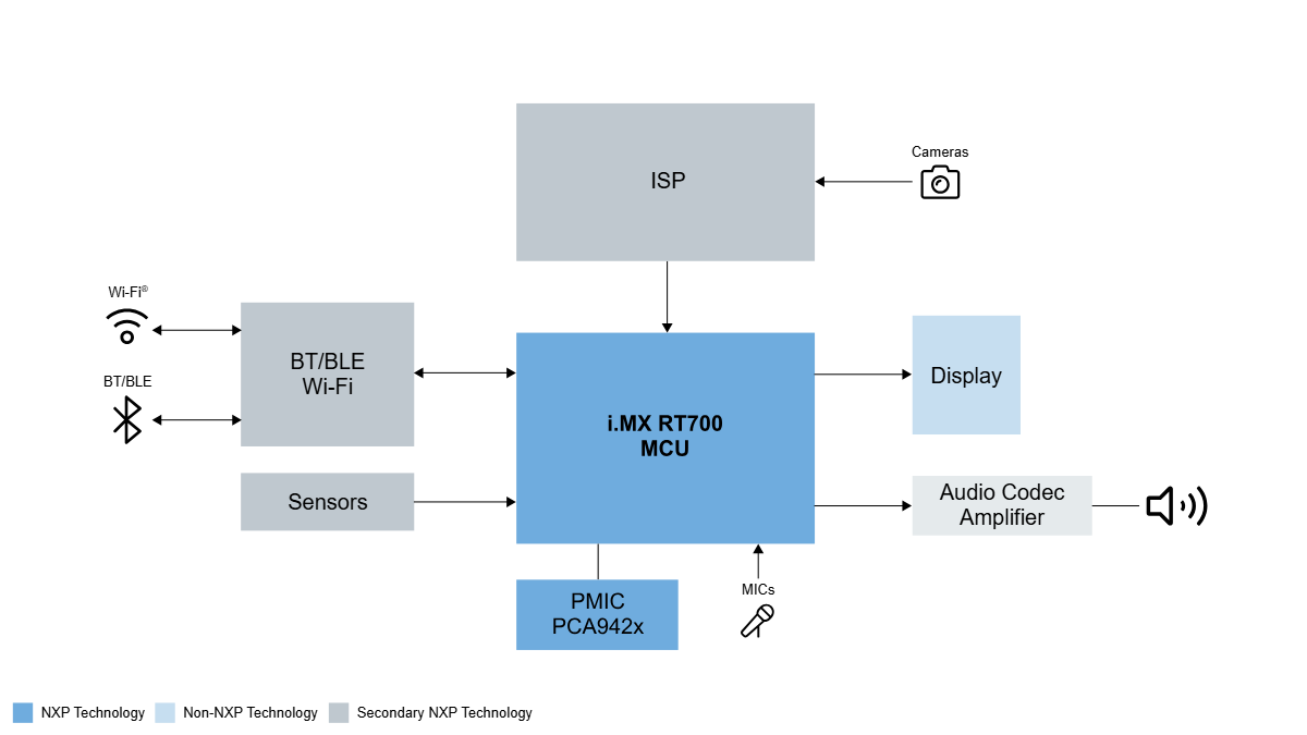
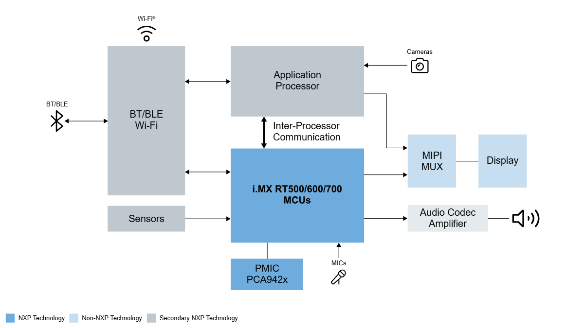
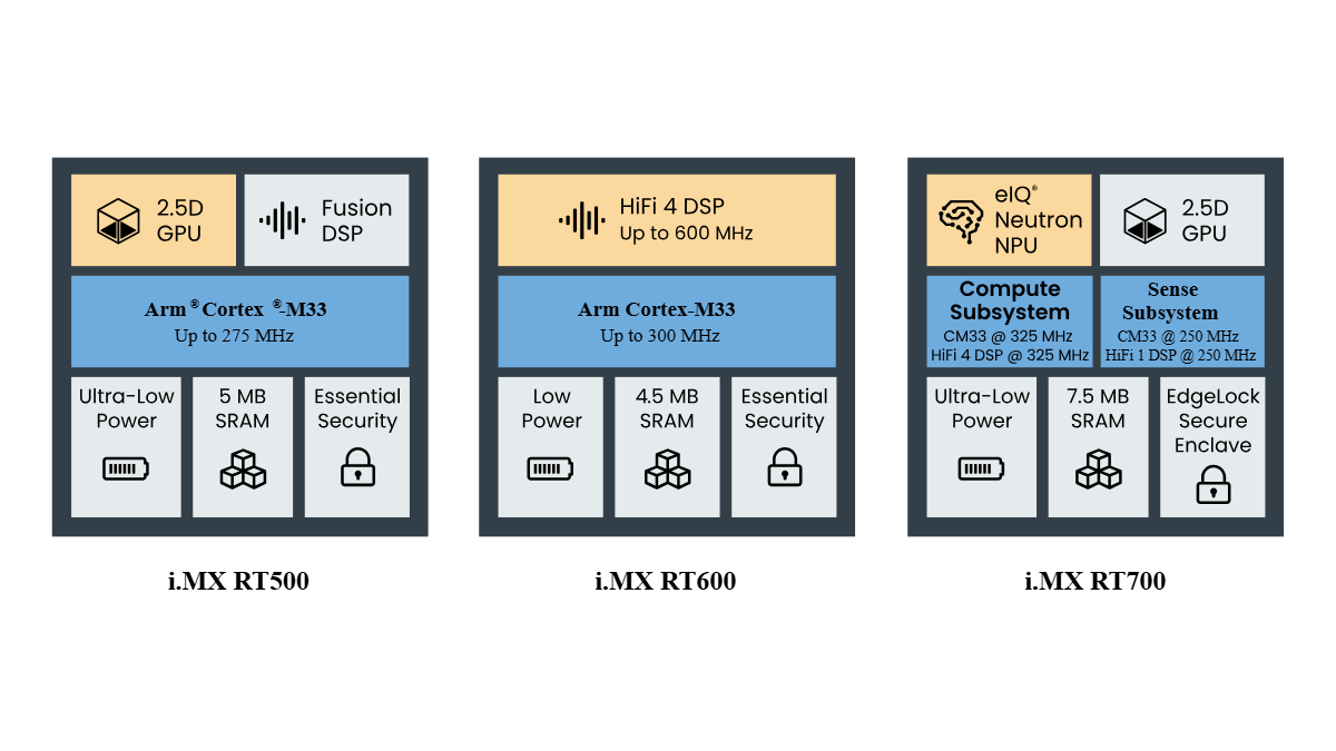
NXP’s Solution: The i.MX RT Family as the Ideal Coprocessor
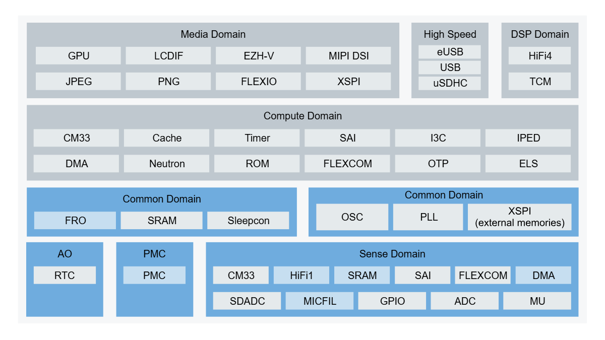
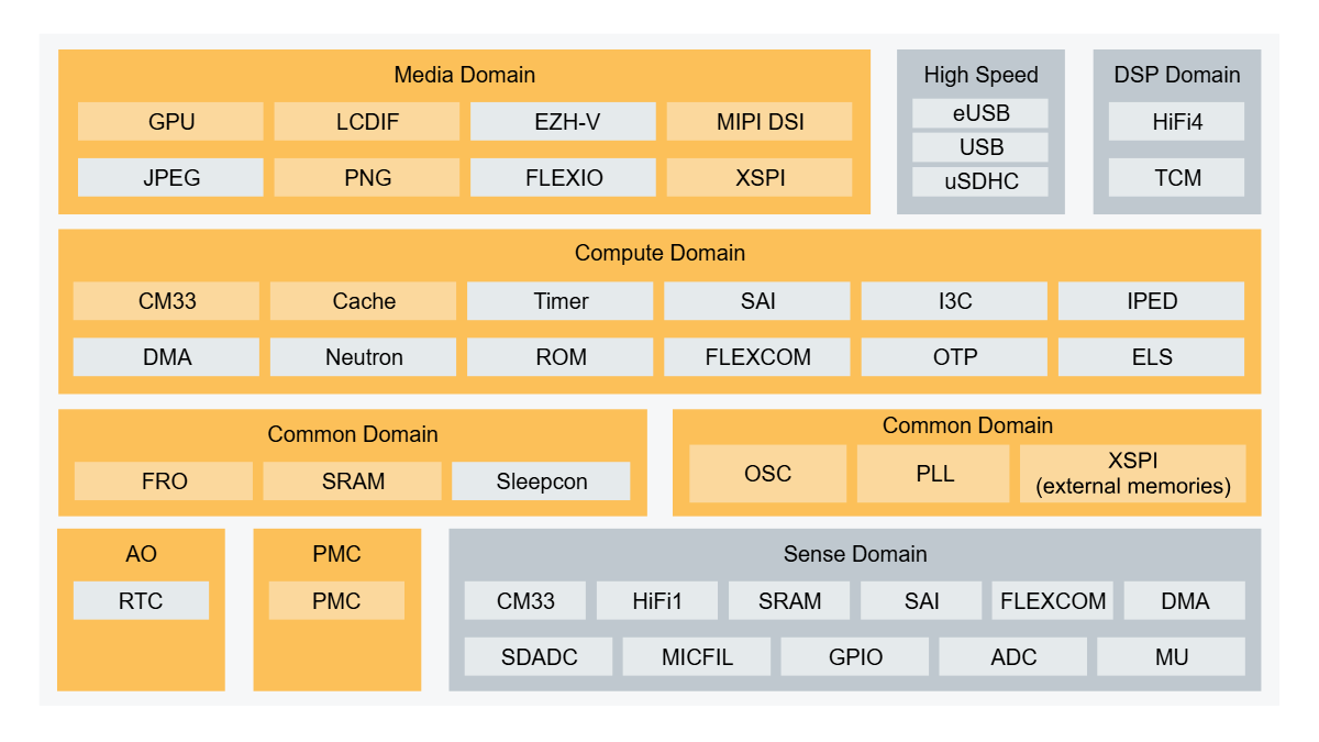
The i.MX RT500, i.MX RT600 and i.MX RT700 has three chips in NXP’s i. MX RT low-power product family. These chips, as coprocessors, are currently widely used in the latest AI eyewear designs for many customers around the world. The i.MX RT500 Fusion F1 DSP can support voice wake-up, music playback, and call functions of smart glasses. The i.MX RT600 is mainly used as an audio coprocessor for smart glasses, supporting most noise reduction, beamforming, and wake-up algorithms. The i.MX RT700 features dual DSP (HiFi4/HiFi1) architecture and supports algorithmic processing of multiple complexities, while enabling greater power savings with the separation of power/clock domains between compute and sense subsystems.
How the i.MX RT700 Maximises Battery Life
As a coprocessor in AI glasses, the i.MX RT700 can flexibly configure power management and clock domains to switch roles based on different application scenarios: it can be used as an AI computing unit for high-performance multimedia data processing, and it can also be used as a voice input sensor hub for data processing in ultra-low power consumption.
AI glasses mainly rely on voice control to achieve user interaction, so voice wake-up is the most commonly used scenario and the key to determining the battery life of AI glasses. In mainstream use cases, the coprocessor remains in active mode at the lowest possible core voltage levels, awaiting the user’s voice commands, quickly switching to speech recognition mode with noise reduction in potentially noisy environments. Based on this user scenario, the i.MX RT700 can be configured to operate in sensor mode; at this time, only a few modules, such as HiFi1 DSP, DMA, MICFIL, SRAM, and power control (PMC), are active. The Digital Audio Interface (MICFIL) allows microphone signal acquisition; DMA is used for microphone signal handling; HiFi1 is used for noise reduction and wake-up algorithm execution, while the compute domain is in a power-down state.
Other low-power technologies included in the RT700, such as distortion-free audio clock source FRO, microphone module FIFO, and hardware voice detection (Hardware VAD), DMA wake-up also ensures that the system power consumption of i.MX RT700 voice wake-up scene can be under 2 mW, maximising power consumption while continuously monitoring.
RT700 also powers MCU-only
For display-related user scenarios, the i.MX RT700 can be configured in “High Performance Mode”, where the Vector Graphics Accelerator (2.5D GPU), Display Controller (LCDIF), and Display Bus (MIPI DSI) are enabled. While enabling high performance, the compute domain also takes advantage of low-power technologies such as MIPI ULPS (Ultra Low Power State), dynamic voltage regulation within the Process Voltage Temperature (PVT) tuning, and other low-power technologies.
With the continuous integration of intelligent hardware and artificial intelligence, choosing the right low-power high-performance chip has become the key to product innovation. With its deep technology accumulation, the i.MX RT series provides a solid foundation for cutting-edge applications such as AI glasses.
The post AI Glasses: Ushering in the Next Generation of Advanced Wearable Technology appeared first on ELE Times.
The semiconductor technology shaping the autonomous driving experience
Courtesy: Texas Instruments
Last summer in Italy, I held my breath as I prepared to drive down a narrow cobblestone road. It was pouring rain with no sign of stopping, and I could hardly see. Still, I pressed the gas pedal, my shoulders tense and my hands gripping the wheel.
This is just one example of a stressful driving experience. Whether it’s enduring a long road trip or crawling through bumper-to-bumper traffic, many people find driving to be nerve-wracking. Though we can spend weeks finding the perfect car, deliberating which seats will feel the most comfortable or which stereo system will sound the richest, it’s hard to enjoy the ride when you are constantly scanning for hazards, adjusting to changing weather conditions, or navigating unknown roadways.
But what if you could appreciate the experience of being in your vehicle while trusting your car to navigate the stressful drives for you?
We’re progressing toward that future, with worldwide investment in autonomous vehicles expected to grow by over US$700 million in 2028. But to understand the vehicle of the future, we must first understand how its architecture is evolving.
How software-defined vehicles (SDVs) are transforming automotive architecture
I can’t discuss the vehicle of the future without starting with the transition to software-defined vehicles (SDVs). Because SDVs have radar, lidar, and camera modules, they are critical to a future where drivers have the latest automated driving features without having to purchase a new vehicle every few years.
For automotive designers, SDVs require separating software development from the hardware, fundamentally changing the way that they build a car. When carmakers consolidate software into fewer electronic control units (ECUs), they can make their vehicle platforms more scalable and streamline over-the-air updates. These ECUs can handle the control of specific autonomous functions in real time, such as automatic braking or self-steering modules.
How integrated sensor fusion enables higher levels of vehicle autonomy
When SDVs centralise software, they’re capable of integrating advanced driver assistance system technologies that enable increased levels of vehicle autonomy. On today’s roads, using the Society of Automotive Engineers’ Levels of Driving Automation, level 1 or 2 (which requires people to drive even when support features are engaged) is the most prevalent. But what about in the future?
I envision that one day, every car will have accurate level 3 or 4 autonomy, characterised by automated driving features that can operate a vehicle under specific conditions. The advances in technology happening now will enable drivers to trust features in future vehicles as much as features like cruise control today. Instead of being fully responsible for stressful driving tasks, we can trust the vehicle’s system to take the lead. And at the heart of this evolution are semiconductors.

To achieve higher levels of vehicle autonomy, the ability to accurately detect and classify objects and respond in real time will require more advanced sensing technologies. The concept of combining data from multiple sensors to capture a comprehensive image of a vehicle’s surroundings is called sensor fusion. For example, if a radar sensor classifies an object as a tree, a second technology, such as lidar or camera, can confirm it in order to communicate to the driver that the tree is 50 feet ahead, enabling swift action.
Why future vehicles need a high-speed, Ethernet-based data backbone
I like to say that tomorrow’s cars are like data centres on wheels, processing multiple large streams of high-speed data seamlessly.
The car’s computer, among other functions, coordinates things such as radar, audio, and data transfer in a high-speed communication network around the vehicle. While legacy communication interfaces for in-vehicle networking, such as Controller Area Network (CAN) and Local Interconnect Network (LIN), remain essential for controlling fundamental vehicle applications such as doors and windows, these interfaces must seamlessly integrate with emerging technologies. In order to accommodate the higher data processing needs of new vehicles, Ethernet will be the prevailing technology. Automotive Ethernet has emerged as a “digital backbone” to efficiently manage applications ranging from audio to standard radar.
As vehicles become capable of higher levels of autonomy, automotive designers will need higher-bandwidth networks for applications including high-resolution video and streaming radar. At TI, our portfolio supports diverse functions with varying requirements, readying us for that network evolution. With technologies like FPD-Link, vehicles can stream uncompressed, high-bandwidth radar, camera, and lidar data to the central compute to respond to events in real-time.
Design engineers must also have a powerful processor in the central computing system that can take data from multiple technologies, such as lidar, camera, and radar sensors, to complete a fast, real-time analysis and provide a 4D data breakdown to better perform object classification.
With expertise in radar, Ethernet, FPD-Link technology and central compute, TI works with automotive designers to help optimise solutions from end to end. Rather than designing devices that only perform one function, we look at how to best optimise our device ecosystem. For example, we design radar devices that easily interface with our Jacinto processors to achieve faster, more accurate decision-making.
What these advancements mean for the future driving experience
In the future, if I encounter the same road and rainy conditions in Italy as I did this summer, I might not drive. Instead, I might trust my car to safely get me to my destination, while I relax in my seat.
The vehicle of the future might not exist yet. But the technologies we’re developing today are making the vehicle of the future – and maybe even the next breakthrough of the future – real.
The post The semiconductor technology shaping the autonomous driving experience appeared first on ELE Times.
Pages

