
Feed aggregator
Space Forge announces completion of UK Space Agency-funded National Microgravity Research Centre
United Semiconductors reserves payload space with Starlab to advance commercial-scale in-space semiconductor manufacturing
I am pretty sure this won't work.
 | It didn't. I am thinking that the flux held this nicely in place until testing identified some issue. [link] [comments] |
🎥 «Історична модель ООН» у КПІ ім. Ігоря Сікорського

У КПІ відбулася Всеукраїнська науково-практична конференція «Історична модель ООН» у форматі освітньо-рольової гри.
Як це працювало на практиці:
КПІ ім. Ігоря Сікорського та Київ Мілітарі Хаб підписали Меморандум про співпрацю

🔵 Київська політехніка та Київ Мілітарі Хаб починають системну взаємодію у сфері ветеранської підтримки.
🤝 Партнерство охоплює:
Custom design PWM filters easily

It’s well known that the main job of a pulse width modulator’s filter is to limit the maximum peak-to-peak amplitude of the fPWM Hz-induced ripple. It attenuates this to a specified fraction—Frac of the full-scale PWM output—while passing PWMavg, the average value of the PWM signal.
Wow the engineering world with your unique design: Design Ideas Submission Guide
Although the duty cycle can change instantaneously, the filter’s response to that change takes time to settle. It’s convenient to define the settling time Tfrac to be that after which the transient response remains within ± Frac of PWMavg. (After fully settling, the response variations will be from the ripple only and will remain within ± Frac/2 of PWMavg.) And it’s generally true that the more the ripple is attenuated, the larger Tfrac is. But for a given filter with two or more poles, there is an infinite number of combinations of component values that will limit the maximum ripple to Frac. (Think of the number of poles as being the number of capacitors in an R – C filter.) And yet the value of Tfrac is typically different for each combination. So we have a filter optimization problem: find the component value combination that minimizes Tfrac while satisfying the ripple requirement Frac.
I’ve addressed this issue before in a Design Idea (DI), but the procedure’s complexity was perhaps off-putting and inadequately flexible. I’ve since revisited the problem, finding a somewhat improved and analytically optimal solution. But that improvement alone does not justify a new DI.
So, why this new DI?What I think does justify this is a spreadsheet that offers greater flexibility in terms of filter requirements and automates all the work for you. Download the files from https://github.com/Christopherrpaul/Customizable-PWM-Filter .
If you use OneDrive or something like it, you must install the files outside the OneDrive folder. (Safely ensconced there, OneDrive doesn’t “see” them and can’t interfere with the spreadsheet’s query of the paths to where certain files are stored locally.)
Open the spreadsheet. In the following, the yellow-highlighted parameters here and on the spreadsheet are inputs to be supplied by the user; the green-highlighted ones are spreadsheet outputs. Tell it your PWM frequency, in Hz, specify the required value of Frac, and press the “Calculate” button.
The Visual Basic Application (VBA)-driven spreadsheet takes that information and determines the values of the filter’s real and complex pole pairs ( the Q and ω0 of the latter ), which give you the optimal, smallest Tfrac, which it also displays.
To produce an implementable filter, it then combines this information with the (default) values of the filter’s capacitors c1, c2, and c3 . (These you can change and again press Calculate.) From all of this, it determines both the exact and the closest standard E96 values for the resistors r1, r2, and r3 needed to complete the filter. The filter itself is the third-order Sallen-Key low-pass depicted in the schematic portion of the spreadsheet screenshot seen in Figure 1.

Figure 1 A screenshot of the spreadsheet that runs the show. See the text.
And since we all like graphs, two have been provided. The one on top shows how ω0 and the real portion of all poles vary with Q. More importantly, it also shows that TFrac generally gets worse (larger) as Q is increased (not surprising, with the concomitant increase in oscillatory amplitudes).
The other graph shows the decay with time of PWMavg minus the absolute value of the transient response, with the voltage displayed on a logarithmic scale. The bumps are evidence of a damped oscillatory behavior.
But as they say in the late-night TV commercials (or at least they used to), “But wait! There’s more!”
How do I know this thing works?You might ask how you can confirm that this filter will perform as advertised. The answer is easy if you’ve installed LTspice on your computer and you tell the spreadsheet the path starting from the root directory to the LTspice.exe file. Mine’s in C:\Users\chris\AppData\Local\Programs\ADI\LTspice\LTspice.exe.
Don’t worry if you can’t see the entire entry in the Excel cell provided. (NOTE – With the discussions surrounding the ongoing changes in LTspice versions 26.x.y, these files have been developed for use with the stable and still widely used LTspice 17.1.15. This version can still be downloaded and installed: https://ltspice.analog.com/software/LTspice64.exe. I haven’t checked if the files work with the 26.x.y versions.)
Press the “LTspice: Exact…” button. It will automatically launch a simulation using the exact resistor values derived and plot the filter’s response to the two biggest transients: a “full” one from 0 to 100% duty cycle (no PWM ripple) and a “half” one from 0 to 50% duty cycle (maximum possible ripple). See Figure 2 for a sample LTspice run.

Figure 2 An LTspice run using Exact component values for a sample filter.
The responses have been offset to reach their final values at 0 V. Tfrac appears on the plot as a vertical line along with two horizontal lines, which are at ± Frac. You can zoom in to see that the value of Tfrac is indeed correct; it crosses a ± Frac line exactly at the point that the full transition response does. (The full transition always takes a little longer to settle than the half-step transition.)
But alas, alack; this assumes perfect components with 0% tolerances. So the “LTspice Standard…” button launches a simulation of 100 Monte Carlo runs with capacitor and resistor tolerances of 1% and 1% using the E96 resistor values. (You can change all three of these default values and re-run the simulation. In fact, it’s worth considering the overall reduced settling time that can be had with suitably chosen 0.1% resistors added in series with small 1% resistors to more closely approach the exactly calculated values. Better tolerance capacitors would also help, but they tend to be prohibitively expensive.)
As you’ll see, non-zero tolerance variations lead to settling times longer than Tfrac. But by performing an extended number of Monte Carlo runs, you’ll be able to determine the time beyond which even filters made out of real-world components will have settled to Frac.
Filter design constraintsThe real portions of all poles in the filter have been constrained to be identical. The reason for this is that these values control the decay rates of the half- and full-step transients, either of which could dictate the overall settling time. Given that the total ripple attenuation is the product of the real parts of both poles, if one were smaller than the other, it would extend the overall settling time beyond that achieved with identical poles. This constraint also simplifies the optimization problem in that there is only one real and one imaginary value of poles to consider, rather than one imaginary and two real values.
Calculated resistor valuesDepending on certain inputs to the spreadsheet, the derived values of the filter resistances might be smaller or larger than you’d like. In that case, the input values of the capacitors could be multiplied by a constant K of your choosing to obtain new resistor values divided by that K.
The spreadsheet’s default capacitor values are in the “Goldilocks” range—large enough that op amp input and PCB capacitances will affect them minimally, but small enough that NPO/COG type capacitors (whose stability with temperature and DC voltages are demanded in filter designs) are not prohibitively expensive. The ratios of one to the other of the default capacitor values have been shown to consistently result in realizable filters. Feel free to experiment with other values and ratios, but be aware that it might not be possible to realize filters with those changes.
Filter driversDo not drive the filter from a microprocessor directly. Its non-PWM functions draw currents that lead to small voltage drops across the IC-to-package-pin bonding wires. These induce errors by preventing signals from getting close to the ground and the supply rail. Instead, buffer the microprocessor with dedicated SN74AC04 logic inverters, which will swing to the rails, since they have no other currents to deal with and their outputs are minimally loaded. For a reasonably accurate reference voltage supplying the SN74AC04, consider the REF35.
SN74AC04-induced errorsIt’s been pointed out that all digital drivers have different logic high and low resistances. These differences are sources of error that are worst at a 50% duty cycle. The part’s data sheet says that at a 3-V supply, the logic high voltage drop under a 12-mA load over the industrial temperature range could be as high as 560 mV, with a resistance of 45 ohms.
The logic low resistance maximum is a bit better, but there is no spec for the difference. The safe but admittedly ridiculous possibility is that the logic low resistance is 0 ohms, leaving us with a 45-ohm difference. This can be mitigated by paralleling G gates to reduce the drive resistance by that factor to produce a difference of Rdiff = 45/G.
Since no DC current can flow through the filter’s passive components, the fractional full-scale error at 50% is:
.5 · r1 / ( r1 + Rdiff) – .5 = – .5 · Rdiff / ( r1 + Rdiff)
For a b-bit PWM, you’d probably want the error to be less than half of one LSbit or 2-b-1. So you’d require that r1 > Rdiff · 2b.
Consider G = 5. For b = 8, r1 > 2300 ohms. For b = 12, it’s 37 kohms, and for b = 16, 590 kohms. But this brings up a second point: a large b means a relatively small fPWM and therefore a large TFrac. Fortunately, there’s a way around this.
Double upSumming the contributions of two 8-bit PWMs, one of whose signals’ amplitude is 256 times that of the other, allows both to have an fPWM 256 times larger than that of a single 16-bit PWM. This yields a TFrac reduced by the same factor. Figure 3 shows one way to employ this approach.

Figure 3 Configuration with independent most significant (MSbit) and least significant (LSbit) 8-bit PWMs, the latter contributing 1/256 of the former, to replace a single 16-bit PWM. This arrangement reduces the settling time by a factor of 256.
Op-amp considerationsFigures 1 and 3 lead to the question of which op amp to use. A rail-to-rail input and output unit is warranted. The OPA376 family of singles, duals, and quads is a good answer.
It’s 25 µV at 25°C, ±1 µV/°C from -40 to +85°C, and barely disturbs the accuracy of even a 16-bit PWM. Its input bias current of 10 pA maximum at 25°C, and its typical (no maximum spec) of less than 50 pA at 85°C, introduces errors on par with its offset voltage. Consider the op amp’s output rail-to-rail limitations, however. Either avoid PWM duty cycles at the extremes, or extend the op amp’s supply rails a few tens of millivolts (see its data sheet) beyond those of the PWM.
In approaching your design, you might find the following nomograph in Figure 4 useful.

Figure 4 The above nomograph can aid in selecting the operating point of your design.
Problems, gripes, suggestions, requests, and accoladesThe spreadsheet employs VBA numerical iteration routines to find the Q, ω0 pairs and the filter resistors. Although I’ve tested these routines extensively, it’s always possible that one or the other will fail to converge with some combination of input values.
In that case, please let me know by adding a note to the “Comments” section of this DI. This will generate an automatic email alert and will allow the inclusion in our conversation of others who might be interested. Please do not email me unless you have a comment that is truly meant to be private (a marriage proposal?) I encourage feedback of all kinds.
A grudging acknowledgementI’d be remiss if I did not mention the help I got from a certain widely available AI program in developing this project. This ranged from deriving Inverse Laplace transforms and Newton-Raphson iteration algorithms to VBA coding.
But working with this AI wasn’t all lollipops and rainbows. In the course of the effort, I was reminded of Ronald Reagan’s admonition to “Trust, but verify.” But as things progressed, I dropped the “trust” part.
I found I had to break tasks down into sections, understand each that was provided, test assiduously, and make corrections before proceeding to the next step. Setting a multi-step task was a recipe for disaster. Still, AI is a valuable tool, and I find it even more valuable now that I better understand how to work with it.
I’d be interested in hearing about others’ experiences.
Related Content
- Gold-plated PWM-control of linear and switching regulators
- Brute force mitigation of PWM Vdd and ground “saturation” errors
- A nice, simple, and reasonably accurate PWM-driven 16-bit DAC
- PWM buck regulator interface generalized design equations
The post Custom design PWM filters easily appeared first on EDN.
NVIDIA announces strategic partnership with Lumentum to develop data-center optics
Simple Trf radio reciever I made
 | I made a simple trf radio reciever using two transistor as class A rf amps,it is not much but it is probably the only project I made without following any instructions,so it's special to me The audio quality is very clear and and the sound is good,it doesn't require any additional audio amplifier if you use standard 32 ohms earphones. (forgive me for the weird proportion of symbols in the diagram) [link] [comments] |
💥 Тиждень математики 2026

З нагоди Міжнародного дня числа Пі та в рамках Всеукраїнського тижня математики КПІ ім.Ігоря Сікорського проведе у закладах загальної середньої освіти з 12 по 18 березня 2026 року комплекс виїзних заходів.
What is Fashion Tech? Providing New Product Value and Customer Experiences with Technology
Courtesy: Murata Electronics
What is fashion tech? – diverse technologies and methods evolving the industry
“Fashion tech” is a term that combines fashion and technology. It refers to the use of big data, artificial intelligence (AI), augmented reality/virtual reality (AR/VR), and IT in customer services; the development of products incorporating functional materials and wearable devices; and the application of electronics and digital technologies in manufacturing, processing, and distribution processes.
Fashion tech is expected to garner even more attention as a means to invigorate future consumption activities, products, industries, and markets as technology progresses and new products and services are introduced. As mentioned earlier, fashion tech is a broad term, but it can be classified into two categories based on its nature. One is the evolution of services and customer experiences (CX), and the other is the evolution of product functionality and manufacturing processes. We explain these two aspects of fashion tech in the following sections.
Fashion tech evolving the customer experience (CX)
IT and digital transformation (DX) are currently driving fashion tech. There have been many challenges in enhancing sales CX in stores and on e-commerce sites, but many of these have been addressed through IT and DX initiatives.
For example, when selling clothing, shoes, jewellery, watches, eyewear, bags, etc., online, a longstanding issue has been the high hurdle for purchase decisions due to the difficulty for individual consumers to imagine how the actual products would look on them. However, in recent years, virtual fitting via AR (augmented reality), which can be easily used with smartphones and tablets, has become widely adopted. Even without 3D data for products, the technology to enable three-dimensional representation in AR using artificial intelligence (AI), if multiple 2D images of the product are prepared, has lowered the barrier to service introduction.
In parallel with virtual fitting, services are now emerging whereby AI assesses how well eyewear and accessories suit a consumer based on the individual’s facial features and the item’s shape and size. These technological advances are driving improvements in CX through the introduction of fashion tech.
Furthermore, the adoption of radio frequency identification (RFID) technology, including RFID tags and readers, is also advancing, and its applications are moving beyond rationalising inventory management. RFID is being used to reduce checkout lines and payment hassles by simplifying self-checkout and protecting brands, such as by authenticating genuine products.
Additionally, AI is being used to analyse customer and consumption trends across physical stores and e-commerce sites using RFID data. This enables a swift response to customer needs through appropriate inventory adjustments. These are just some of the ways technology is being used.
Fashion tech is evolving product value and manufacturing processes through technology
The DX and CX-oriented fashion tech mentioned above is expected to develop further. In addition, fashion tech that provides new added value to consumers through new characteristics and functions of materials and products is likely to garner more attention in the future due to advancements in materials, wearable devices, engineering, and manufacturing processes.
Here, we introduce technologies such as digital fabrication, smart textiles, smart fabrics, and wearables, which are said to be key to the future development of fashion tech.
Digital fabrication
Digital fabrication is a general term for technologies that make or process products based on digital data. In fashion product manufacturing, it refers to using 3D scanners and 3D CAD to digitise product ideas and patterns and then importing the digitised data into digital manufacturing machines such as 3D printers and laser cutters to shape or process the ideas and patterns.
Digital fabrication has attracted attention in recent years due to the diversification of needs and the development of digital technologies. By streamlining the design and manufacturing processes, digital fabrication has made it possible to accommodate high-mix, low-volume production and the manufacturing of personalised products. It is also gaining attention as a technology for providing new added value to products, such as the manufacturing and processing of materials with structures, functions, and properties that were not previously available.
Smart fabrics (smart textiles)
Expectations are rising for smart fabrics or smart textiles (hereinafter, smart fabrics), technologies that create new added value by imparting functionality to fashion products’ materials themselves. The digital fabrication mentioned earlier is also a means to realise these technologies.
Smart fabrics generally refer to imparting functionality to fibres by integrating electronic technology. The functions are diverse. For example, the clothing itself may function as a sensor to monitor the wearer’s health condition, use electricity for sterilisation, or regulate temperature. Various R&D and commercialisation efforts are underway to realise these functions.
Many of these technologies are attracting attention for a wide range of purposes, such as health and medical care, sports and fitness, and safety improvement. The introduction of such technologies into everyday clothing is being plotted to provide new added value through fashion products with advanced functionality.
Wearable and flexible electronics
The integration of wearable devices into fashion items and the IoT-ization of fashion items themselves are also anticipated as a technology closely related to smart fabrics. For instance, by using wearable devices to process, communicate, display, manipulate, and control data sensed by smart fabrics, products could be endowed with a variety of functions and performance.
Many wearable devices, such as smartwatches, have rigid mounting boards and housings, which is fine for wristwatches. However, these rigid components can interfere with body movement and risk device damage when implemented in wearable items such as clothing.
One promising solution to such challenges is flexible electronics. Flexible electronics refer to pliable electronic circuits and components that can bend. This high compatibility with smart fabrics and wearables raises expectations for their application to future fashion tech and the sophistication of functions it will bring.
Fashion trends cyclically go through revivals. It is hard to imagine that futuristic designs like something out of a sci-fi movie will suddenly become mainstream. This is likely because established designs are rational and fit most people’s sensibilities. On the other hand, while the outward appearance of items may follow traditional lines, the purchasing experience, product functionality, and added value will continue to evolve through fashion tech.
The post What is Fashion Tech? Providing New Product Value and Customer Experiences with Technology appeared first on ELE Times.
Plant pulse sensors: From soil probes to tree tattoos

Plants do not just grow—they signal. From the subtle moisture shifts in soil to the faint electrical rhythms coursing through leaves and stems, botanical sensors are turning greenery into living data networks.
What began with rugged soil probes has evolved into delicate tree tattoos that map physiological responses in real time. This convergence of biology and electronics is redefining how engineers, agronomists, and hobbyists alike monitor plant health, optimize yields, and even explore new frontiers in bio-inspired design.
Botanical sensors: Giving plants a voice
The term botanical sensor is best understood as an umbrella category rather than a single device. In agricultural technology (AgTech) and plant biology, it encompasses a wide range of instruments designed to monitor plant health and surrounding environmental conditions in real time.
In essence, these sensors give plants a “voice,” allowing them to signal their needs before visible stress, such as wilting, occurs. Unlike conventional weather stations that measure only ambient air, botanical sensors often interface directly with plant physiology or the immediate root zone, capturing data at the source of growth.
Beyond the broad category, it’s useful to distinguish between two key subtypes. In-plant sensors (often called plant wearables) are tiny, flexible devices attached directly to leaves or stems, enabling close monitoring of physiological signals.
In contrast, soil and root micro-environment sensors operate within the rhizosphere—the soil zone surrounding the roots—capturing data on moisture, nutrients, and microbial activity. These complementary approaches provide a layered view of plant health, and we will explore them in greater depth in the next session.

Figure 1 Visualizing plant–sensor interaction: leaf-mounted and root-zone probes capture real-time physiological data. Source: Author
Plant monitoring sensors: Soil, trunk, and surface frontiers
In principle, there is a wide variety of sensors designed to monitor everything from a small succulent on your table to a massive sequoia in a forest. Among these, soil-based sensors are the ones most often found in homes and farms. Rather than measuring the plant directly, they focus on the environment around the roots, where growth truly begins.
Moisture and conductivity sensors reveal water levels and soil salinity, offering insight into nutrient and fertilizer availability. Here, pH sensors track soil acidity, ensuring that nutrients are in a form the plant can actually absorb. Taken together, these instruments provide a root-level perspective that helps growers fine-tune conditions for healthier, more resilient plants.

Figure 2 The multi-parameter root zone soil sensor measures moisture, temperature, and electrical conductivity. Source: Delta-T Devices
For trees and large-scale agriculture, researchers often turn to sensors that measure the pulse of the plant directly. Sap-flow sensors, for instance, are needle probes inserted into the trunk to track how quickly water moves upward—essentially a heart rate monitor for a tree. Dendrometers capture the subtle micro-expansions and contractions of the trunk, revealing how trees shrink slightly during the day as they consume water and swell again at night.
Infrared leaf-temperature sensors add another layer of insight, detecting whether a leaf is sweating through transpiration. When leaves overheat, it usually signals stress: the plant has closed its pores to conserve water. Together, these devices provide a dynamic picture of plant physiology, extending monitoring beyond the soil to the living tissue itself.

Figure 3 The SFM‑5 sap flow sensor enables minimally invasive, high‑precision measurements of sap flow and sapwood water content in most tree species. Source: UGT
Notably, a newer frontier in plant monitoring involves sensors that adhere directly to the plant’s surface, much like a simple patch or sticker. Graphene tattoo sensors are ultra-thin films that can be taped to a leaf, tracking water loss (transpiration) in real time without causing harm.
Biosignal monitors go further, measuring the electrical signals coursing through plant tissue—essentially listening to how a plant reacts to pests, drought, or other stressors before any visible symptoms appear. While these technologies remain largely experimental, they represent an exciting shift from soil and trunk measurements to direct, non-invasive monitoring of plant physiology, offering a glimpse of how future growers may detect stress before it becomes visible.
In essence, there are so many sensors designed to capture a plant’s vital signs. Stomatal aperture reveals how widely the pores are open, regulating gas exchange and water loss. Sap flow tracks the speed at which water and nutrients move through the stem, a direct measure of circulation. Volatile organic compounds serve as chemical distress signals, emitted when plants face pests or disease.
Volumetric water content pinpoints the precise amount of water available in the soil, while electrical conductivity provides a proxy for salinity and nutrient levels. Together, these parameters form a concise diagnostic suite, offering a snapshot of plant health from root hydration to stress signaling.
On a related note, chlorophyll sensor provides a direct measure of a plant’s photosynthetic capacity by gauging how much light is absorbed or reflected by leaves. Handheld meters and clip-on probes often use fluorescence or reflectance techniques to estimate chlorophyll content, which correlates strongly with nitrogen status and overall plant health.
Because chlorophyll levels drop under nutrient deficiency or stress, these sensors are widely used in precision agriculture to guide fertilization decisions and monitor crop vigor. Unlike soil or trunk sensors, chlorophyll sensors give an immediate snapshot of the leaf’s metabolic activity, making them a practical complement to water and nutrient monitoring systems.
Beyond electronic devices, there is also the emerging field of phytosensing, where plants themselves are engineered to act as living detectors. In this approach, a plant might be genetically modified to change color when it encounters a specific toxin in the soil, effectively turning its physiology into a visible alarm system. Phytosensing highlights a future where monitoring does not just rely on external instruments but on the plants’ own biology, transforming them into active participants in environmental sensing.
Connecting the sensors: Interfaces in practice
In practice, mainstream plant monitoring sensors rely on straightforward electrical connections and increasingly on wireless interfaces that tie them into larger IoT systems. Simple moisture probes output analog signals—usually variable voltage or resistance—requiring external circuitry for signal processing and interpretation.
More advanced probes, such as those for pH or electrical conductivity, typically use digital buses like I²C, SPI, or UART, which provide cleaner signals and allow multiple sensors to share the same wiring. Sap-flow sensors, by contrast, generate heat pulses and require timing circuits to measure how quickly the signal moves through the stem, while infrared leaf-temperature sensors may deliver either analog voltages or digital packets depending on design.
Once signals are captured, a microcontroller acts as a hub to convert raw data into usable readings. From there, connectivity options expand: Wi-Fi and Bluetooth are common in greenhouses or indoor setups, while LoRaWAN and Zigbee provide long-range or mesh networking for large farms.
Data is then routed to cloud platforms or local dashboards, where growers can visualize soil moisture, salinity, or canopy stress in real time. Interfaces range from simple panel displays in the field to mobile apps and web dashboards that log trends and trigger alerts.
Practical considerations remain central: sensors must be calibrated regularly, especially EC and pH probes; outdoor devices need waterproofing and corrosion resistance; and power supplies often rely on batteries supplemented by solar trickle charging. The choice of interface—analog, digital, or wireless—depends on scale and cost, but the goal is the same: to make plant vital signs accessible, reliable, and actionable for growers.
Precision agriculture: The IC ecosystem for botanical monitoring
Modern agricultural sensing integrates a diverse set of specialized ICs to track the vital signs of plants. For soil health, the AD5941 precision A/D converter provides advanced impedance spectroscopy capabilities, enabling high-precision moisture and salinity analysis. It also serves as a modern successor platform for electrochemical pH and nutrient testing when paired with suitable sensor electrodes.
Atmospheric monitoring is led by the SHT4x sensors for humidity and the SCD4x sensors for compact photoacoustic CO₂ detection, while BME688 combines gas sensing with integrated AI to detect volatile organic compounds (VOCs) that can signal plant stress.
Light sensing remains critical: the TCS3448 spectral sensor captures multiple wavelength bands, allowing quantification of photosynthetically active radiation (PAR) and enabling growers to fine-tune light recipes for photosynthesis.
Together, these modern ICs transform plant monitoring from guesswork into data-driven precision, optimizing irrigation, nutrient management, and environmental control.

Figure 4 The BME688 module empowers makers and hobbyists to build minimally invasive, AI-driven plant stress monitors through volatile organic compound detection. Source: M5Stack Technology
Closing note
Admittedly, even a jam-packed post cannot do full justice to the fundamentals and applications of botanical sensors. Much remains to be explored before the puzzle is complete—new sensor models, evolving standards, and emerging use cases continue to reshape the field.
Stay tuned for more. Future installments will dive deeper into canopy-level sensing, chlorophyll fluorescence, microclimate monitoring, and innovative energy harvesters that power sensors autonomously. We will also explore how AI-driven analytics can transform raw sensor data into actionable insights for agriculture, forestry, and ecological research.
This overview offers a snapshot of where plant sensing technology stands today, with the promise of richer insights to follow. If you are fascinated by the evolving world of botanical sensors, follow along and join the conversation—together, we will piece the puzzle into a complete picture of plant sensing technology.
 T. K. Hareendran is a self-taught electronics enthusiast with a strong passion for innovative circuit design and hands-on technology. He develops both experimental and practical electronic projects, documenting and sharing his work to support fellow tinkerers and learners. Beyond the workbench, he dedicates time to technical writing and hardware evaluations to contribute meaningfully to the maker community.
Related Content
- Leaf Wetness Sensor DIY
- Protecting the climate with gas sensors
- Unleashing the power of environmental sensors
- Wearable sensors for plants measure water use in crops
- Environmental sensors transform smart factory systems
The post Plant pulse sensors: From soil probes to tree tattoos appeared first on EDN.
Rio Tinto to progress gallium R&D project by constructing pilot plant in Québec
НН ІАТЕ. Історія та сьогодення

Цього року Навчально-науковий інститут атомної та теплової енергетики (НН ІАТЕ ), створений на базі теплоенергетичного факультету КПІ ім. Ігоря Сікорського, відзначає своє 95-річчя. Адже засновано його було ще 1931 року, коли у складі Київського енергетичного інституту (КЕІ) організували дві кафедри: парових двигунів і теплосилових установок, які стали основою для створення теплотехнічного факультету (ТФ), який з часом став теплоенергетичним (ТЕФ).
Soitec and NTU Singapore reporting results of research program into 6G connectivity
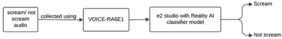
Emergency Screaming Detection: How AI Recognizes Human Screams and Saves Lives
Courtesy: Renesas
Detecting human screams for help is important in disaster relief, security, and healthcare applications. Imagine being stuck in an elevator when the usual means of communication failed. An emergency screaming detection system can recognise the distress signal and immediately activate emergency protocols, such as alerting security personnel or triggering an alarm, to efficiently get help and save lives.
Renesas’ Reality AI Emergency Scream Detection is a machine learning (ML) model designed to identify human screams. This model isn’t just about recognising any loud noise; it’s finely tuned to discern distress calls (as a scream) from background sounds. This system will enable immediate dispatch for help, especially important in enclosed or isolated environments where safety is critical.
How does Emergency Screaming Detection work?
The emergency scream detection system is trained to differentiate different audio sounds based on the data collected. The steps involved in developing this machine learning model are as follows:
- Data Collection and Training: The model’s training begins with comprehensive data collection. A public dataset including a variety of audio samples is used. The “Scream” class, featuring intense nonverbal screaming sounds and screaming with words, is used to train the emergency scream detection system. To ensure the model distinguishes what isn’t a scream, a diverse range of sounds such as wind, ambient noise, normal conversation, singing, music, and clapping is also used from the same dataset.
- Feature Extraction: The next step is to extract meaningful features from the audio files that help the model recognise scream-specific patterns amidst various noises.
- Model Training: After selecting the best feature, a machine learning classifier is trained to distinguish between “scream” and “non-scream” audios. The training process involves adjusting the model parameters to minimise errors and enhance its performance.
By using these methods, the emergency scream detection system can be built to ensure emergency responses are swift, providing a vital safeguard in various environments.
Application Example
Audio signals are collected from the real-world environment to create the Renesas VOICE-RA6E1 Voice User Demonstration Kit. These audio signals are then processed by Renesas’ Reality AI-trained classifier model, which helps in distinguishing between “scream” and “non-scream” audio sounds.
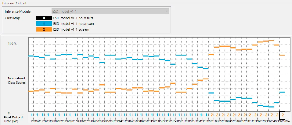
The live testing of Renesas’ Emergency Scream Detection model is benchmarked with ≥90% accuracy for screams at a maximum distance of 2 meters from the testing board. The testing conditions also included background noises such as wind, elevator music, human conversations, baby cries, and ringing phones to determine distress signals while maintaining accuracy.
Easily Build the Application Example
Users can collect audio signals with Renesas’ e² studio IDE and integrate any AI model generated from Renesas’ Reality AI software. After collecting data from a public dataset*, deploy the Reality AI software’s tools to perform feature extraction, model training, and deployment of the model to C code.
The deployed model can be integrated for live testing using the e² studio IDE. After integration, the model can be extensively tested in a live setting using the VOICE-RA6E1 board, and the live results can be visualised using the AI live monitor.
Experience the seamless and fast integration capabilities of Renesas’ Reality AI software and e² studio IDE in model training, deployment, and testing of an application.
Conclusion
The Reality AI Emergency Scream Detection application exemplifies the potential of machine learning in enhancing safety measures in various settings and demonstrates how users can employ Renesas’ technology to integrate advanced feature extraction, model training, and deployment with real-time response capabilities. The scalable Reality AI Tools can generate ML models for a wide range of Renesas MCU and MPU devices.
The post Emergency Screaming Detection: How AI Recognizes Human Screams and Saves Lives appeared first on ELE Times.
India’s Electronics Push: Ambition Is Clear. Execution Will Decide the Outcome
India’s electronics story has entered a decisive phase. The policy announcements of February 2026 — combined with export milestones and strategic partnerships — suggest that the country is attempting something far larger than incremental industrial growth. It is trying to reposition itself in the global technology hierarchy. But ambition alone will not secure that position. Execution will.
The Union Budget 2026–27 allocated ₹40,000 crore to strengthen domestic component manufacturing under the Electronics Components Manufacturing Scheme. This is a necessary correction. For years, India has excelled at assembling finished goods while importing critical components.
Simultaneously, India Semiconductor Mission 2.0 signalled a deeper commitment to building semiconductor capability across fabrication, assembly, and materials. The intent is clear: India does not want to remain at the lower end of the value chain.
The export data reinforces this shift. Smartphone exports have touched roughly $30 billion, with global leaders such as Apple and Samsung Electronics scaling manufacturing operations in India. This is not a small achievement. In less than a decade, India has moved from a peripheral manufacturing base to a meaningful node in global electronics supply chains.
Yet, the central question remains: Is India building depth — or scale without control?
Assembly success does not automatically translate into technological sovereignty. True leverage lies in advanced semiconductor fabrication, high-end equipment manufacturing, precision materials, and ownership of intellectual property. On these fronts, India still trails global leaders by a wide margin.
The partnership between Qualcomm and Tata Electronics in automotive electronics demonstrates progress in value-added manufacturing. But automotive modules, while strategically important, are not the same as owning leading-edge fabrication technology.
There is also a structural reality policymakers must confront: semiconductor ecosystems take decades to mature. They require uninterrupted capital flow, stable policy frameworks, reliable power, water security, efficient logistics, and depth in engineering. Any inconsistency could stall momentum.
The global semiconductor race is no longer an economic contest. It is a geopolitical war — one fought with export controls, subsidy regimes, technology blockades, and supply chain realignments. The United States has weaponised semiconductor policy through export controls and industrial subsidies. China has doubled down on domestic chip independence. Europe is pouring billions into sovereign fabrication capacity. Taiwan remains indispensable. South Korea protects its giants as strategic assets.
Semiconductors have become the oil of the digital century — and nations are securing supply at any cost.
What India is attempting is bold — and necessary. Electronics today underpin defence systems, AI infrastructure, mobility platforms, and digital economies. Countries that control semiconductor depth control strategic autonomy.
The danger is complacency born from export success. Hitting $30 billion in smartphone exports is impressive. But if core chips, advanced lithography systems, and high-value IP remain imported, strategic vulnerability persists.
India’s electronics sector is at a crossroads. The past month shows strong policy intent and rising industrial confidence. The next five years will test whether this momentum can be translated into irreversible capability.
The world is reorganising supply chains. India has an opportunity to claim a durable position. But the window will not remain open indefinitely. Ambition has been declared. Now comes the harder task — building capability that the world cannot bypass.
The next ten years will determine whether India becomes: a swing state in the global tech war, a protected assembly corridor or a sovereign semiconductor power. The chip war is not theoretical. It is unfolding in export controls, trade negotiations, and defence alliances.
The question now is whether it is prepared to fight at the highest technological tier — or remain a strategic subcontractor in someone else’s supply chain.
History will not remember the announcements. It will remember who controlled the chips.
Devendra Kumar
Editor
The post India’s Electronics Push: Ambition Is Clear. Execution Will Decide the Outcome appeared first on ELE Times.
India on the Road to Semicon Self-Reliance with Three More Plants
India to welcome three more semiconductor plants after PM Modi inaugurated Micron’s plant last week, on February 28.
Since the commencement of the India Semiconductor Mission in 2021, India has developed its semiconductor ecosystem exponentially, with four out of ten plants already approved and three more to be inaugurated in 2026 itself. The government further accelerated this by introducing catalyst initiatives like the PLI scheme.
With semiconductors being the core of any modern technology, the demand has grown multifold, and India is pioneering to become a competitive manufacturer for semiconductor to meet the global demand.
India has given approval to ten semiconductor plants in six states with an investment of about Rs 1.60 lakh crore.
As per government records, the approved list of semiconductor plants other than the recently inaugurated Micron plant is as follows:-
- Tata Electronics (Dholera, Gujarat): Semiconductor fab in partnership with PSMC, Taiwan.
- CG Power (Sanand, Gujarat): OSAT facility in partnership with Renesas & Stars.
- Tata Semiconductor Assembly and Test (TSAT) (Morigaon, Assam): Semiconductor packaging facility.
- Kaynes Semicon Pvt Ltd (Sanand, Gujarat): OSAT facility.
- HCL-Foxconn JV (Location TBD): Semiconductor packaging and testing.
- SiCSem Private Limited: Compound semiconductor manufacturing.
- 3D Glass Solutions Inc.: Advanced substrate manufacturing.
- Advanced System in Package (ASIP) Technologies: Assembly and testing.
- Continental Device India Private Limited (CDIL): Discrete semiconductor fab.
The evolving semiconductor landscape in India is expected to generate over two lakh jobs, secure supply chains, as well as strengthen the AI, EV, and defence sectors.
By: Shreya Bansal, Sub-Editor
The post India on the Road to Semicon Self-Reliance with Three More Plants appeared first on ELE Times.
Veeco books multi-system Lumina and Spector orders for InP datacom laser manufacturing
Board-in interconnects
 | submitted by /u/1Davide [link] [comments] |
ams OSRAM completes sale of Entertainment & Industry Lamps business to Ushio for €114m
Pages


![[link]](https://i.redd.it/b3q3r59mdumg1.png)
![[link]](https://i.redd.it/3j15hxy23omg1.jpeg)