
Feed aggregator
Perusing a LED-based gel nail polish UV lamp

This engineer doesn’t use nail polish, but his wife does. And he deals with plenty of PCBs. What do these things have in common? Read on.
Speaking of LEDs that lose their original intensity over time and use…
In the fall of 2020, after accepting that due to the COVID pandemic she wasn’t going to be getting back inside a nail salon any time soon, my wife invested in a UV lamp so she could do her own gel polish-based nails at home. While the terminology I just used in the prior sentence, not to mention the writeup title that preceded it, might be “old news” to at least some of you, others (like me, at first) might be confused. Here goes:
Gel detailsFirst off, what is gel nail polish, both in an absolute sense and relative to its traditional counterpart? Here’s manufacturer OPI’s take:
A gel manicure is a coat of colored gel that looks deceptively similar to nail polish. It’s a thin brush-on formula, designed for high performance and a glossier finish than regular nail polish…An OPI GelColor manicure [also] lasts for up to 3 weeks…The primary difference between gel nails and a regular manicure is curing. Between each coat, you cure the color and set the gel nail polish by putting your nails under a special light.
That “special light” is a UV lamp. Initially, they were constructed using fluorescent tubes. But nowadays, mirroring the broader trend, they increasingly use LEDs instead. The one my wife first bought is Bolasen’s SunX Plus, a “Professional True 80W Salon Grade LED Nail Dryer for Gel Polish.” The link to it on Amazon’s main site now auto-forwards to a more recent battery-operated model (this one’s AC-powered), but I found a still-live product page copy on Amazon’s South Africa site (believe it or not). Here’s the associated stock artwork:

I’m not sure I want to know what the “no black hands” phrase references…


The black base shown in the stock images is missing in action; my wife found that foregoing the bottom plate expanded the lamp’s extremity-insertion gap spacing, thereby easing use. More generally, she’s now replaced this initial UV lamp with a newer successor; the original device’s intensity apparently faded over time, eventually taking excessively long to work its drying magic.
Polymer processingSpeaking of drying (or if you prefer, curing), what’s so special about UV light? Over to a blog post at the Manicurist website for an explanation:
Whether LED or UV, these lamps emit ultraviolet (UV) rays that trigger a chemical reaction called “polymerization”. Under UV exposure, the molecules in the polish bond together to form a solid and durable film known as a “polymer network”.
UV curing is more broadly used in a variety of applications and industries, as Wikipedia notes:
UV curing (ultraviolet curing) is the process by which ultraviolet light initiates a photochemical reaction that generates a crosslinked network of polymers through radical polymerization or cationic polymerization. UV curing is adaptable to printing, coating, decorating, stereolithography, and in the assembly of a variety of products and materials. UV curing is a low-temperature, high speed, and solventless process as curing occurs via polymerization. Originally introduced in the 1960s, this technology has streamlined and increased automation in many industries in the manufacturing sector.
More generally, electrical engineers out there will likely be particularly interested, for example, in UV light’s key role in the photolithography process used to make printed circuit boards!
So why, if this is a UV lamp that’s supposedly emitting light beyond the visible spectrum, is its output discernible by the human visual system (along with my smartphone’s camera)?

(cool photo, eh?)
Part of the answer may be that the LEDs in the design aren’t true UV at all, but instead leverage the lower-cost alternative referred to as near-UV. Part of it may be that the output spectral plot is sufficiently broad to still-noticeably “leak” into the violet portion of the visible range. And part of it may be that, to reassure users that the device is “on” (thereby preventing lengthy periods of peering at “pure” UV light, with likely retinal-damage consequences), the LED manufacturer added a phosphor layer to additionally generate a visible light output. Hold that thought.
Power spec uncertaintyLast (but definitely not least), before diving in, what’s with that “80W” output claim? The device actually supports two different power output modes, 80W and “low-heat” 55W, user-selectable via one of the four topside switches. When I initially plugged the lamp in without the LEDs illuminated, my Kill A Watt electricity usage meter measured 1W of power consumption:

Switch the LEDs on, in low-output mode, and I got 12W:

And in “high” mode? 23W:

12W ≠ 55W. And 23W ≠ 80W. So, what gives? At first, I wasn’t confident that my Kill A Watt was measuring power consumption correctly. But then I looked at the “wall part” that powers the lamp (in the first image of the sequence that follows, as with subsequent images in this post, accompanied by a 0.75″, i.e., 19.1 mm diameter U.S. penny for size comparison purposes):


Let’s zoom in on that last one:

Unless my math’s totally whacked, 24V times 1.5A equals 36W, not 80W, far from higher than that (to account for consumption inefficiency). So again, what gives? Was Bolasen’s marketing team being flat-out deceiving? Maybe: my cynical side certainly resonates with that conclusion.
But at the end of the day, I’ve decided to give the company the benefit of the doubt and conclude that, just as LED light bulb manufacturers do in spec’ing their devices vs incandescent precursors, Bolasen is using fluorescent UV tube intensity equivalents in rating its LED-based UV device. Online references I’ve found equate the lumens brightness rating of a 20-plus watt LED to that of an 80W fluorescent tube. Granted, that’s for visible light, but perhaps the comparison holds in the ultraviolet band as well…regardless, let me know your thoughts in the comments!
Diving insideMy background-info pontification now concluded (thank goodness, right?), let’s get to tearing down, shall we? Here’s our patient:


Raise the transport handle!


FCC-certified? Really? Call me cynical (again):


The specs say 42 total “beads” (LEDs). That matches my count in the photo that follows:

Look closely and you’ll also see, among other things, five screw heads, which I’m wagering are our pathway inside, along with an array of passive ventilation holes. Here’s the 12-LED cluster at the top (when the device is in its normal operating orientation, that is):

and the cluster-of-six at the back:

Along each side are four more clusters-of-three, such as this one:

The ones at either end, i.e., straddling the lamp’s opening in its normal orientation, are special. The one at the right side (again, in normal orientation) also includes an IR (infrared) transmitter:
![]()
while the other additionally incorporates an IR receiver:

This, dear readers, is how the lamp implements the following function (quoting the original broken English on the Amazon product page):
Use the auto-sensor, it would turn on or off automatically when you put hand/foot in or out.

Insert your appendage (hand or foot, to be precise), and its presence breaks the infrared beam that normally traverses the transmitter-to-receiver gap in an uninterrupted fashion. Voila!
OK, let’s get those five screws outta there:

and with only a bit of remaining prying to do:

we’re in!

Although this original lamp may now be too slow to operate for my wife to tolerate, it still works. I’d therefore prefer to put it back together still fully functional and then donate it for someone else to use…or maybe I’ll keep it and use it to cure resin or…hey…make my own PCBs! Regardless, I’m keeping the internal wiring intact. Don’t worry, we’ll still be able to see its guts a’plenty. Let’s start with the inside of the top half of the chassis:

The power connector pops right out of its usual location:


Now for that PCB in the center:


At left is the two-wire connection that powers the LED array. At right is the power input. And the four-wire harness coming out the bottom feeds (and is fed by) the IR transmitter and receiver. The 14-lead IC PCB-labeled U1 in the upper right corner is unmarked, alas, but is presumably the system “brains”. And at lower left is a P60NF03 n-channel MOSFET likely employed for both LED power switching and variable voltage generation (for both “80W” and “55W” modes) purposes.
Flip the PCB over:


and what now emerges into view is the multi-digit eight-segment display along with the four-switch control cluster.
Beating the heatNow for the inside of the other (lower) half. Wow, look at all those thermal-dissipating metal plates (operating in conjunction with the earlier-mentioned passive ventilation array)!

First off, here are the connections to the IR transmitter:
![]()
and IR receiver:

Now for the LED power distribution network. The two-wire harness coming from the PCB first routes to the three-LED plate that’s in the lower left, just below the six-LED plate, in the earlier overview photo:


From there it splits in two directions. The “upper” (for lack of a better word) span first routes to the aforementioned six-LED plate:

Then to a series of three mid-span three-LED plates:

And finally, to a three-LED plate at the end in proximity to the IR receiver:

The “lower” span also then cycles through its own set of three three-LED plates, the last of them alongside the IR transmitter, and terminates at the 12-LED cluster:


These one more aspect to this design that I want to make sure I highlight, which keen-eyed readers may have already noticed. Check out this closeup of one of the LED “beads”:

The yellow tint is reflective of the thin phosphor layer applied to the inside of the “bead” dome to assist in generating augmented visible light for user-operation-stupidity-prevention purposes. But peer underneath it…are there two die in there? Indeed, there are. I’d originally thought I was instead just looking at the LED’s leadframe structure:

but, in the comments to a teardown video of a different UV lamp by “Big Clive” (whose always-excellent work I’ve showcased before):
was an enlightening insight from “restorer19”:
I have the 6-led UV panel you did a video on years ago, from the same brand, and it likely uses the same LEDs – I’ve sacrificed once of the LED chips and an additional one of the phosphor domes/blobs. It appears to have two LED dies on each chip, one bonded with two wires to each end of the module, and one bonded directly downward with only one bond wire leading to it. The 2-wire die (presumably 405nm) lights a visible purple at a lower voltage (just under 3V), and the 1-wire die takes greater voltage to light up. The 1-wire die looks identical to the large one in a 365-nm LED flashlight I recently bought – the surface of the die itself seems to phosphoresce in white, and any color from the semiconductor itself is invisible. Looking at an individual LED module under magnification while powered at about 3.2V makes the two different dies obvious without being too bright to look at.
“Big Clive” had done an earlier teardown of a more elementary UV lamp containing these same dual-die LEDs (this video is, I believe, the same one that “restorer19” was referring to):
wherein he’d conjectured (at least as I interpreted his comments) that the white color, i.e. full-visible-spectrum-when-illuminated die inside might purely be for “powered on” visual user-reassurance purposes. However, a Google search using the phrase “dual die UV LED” produced an interesting (at least to me) AI Overview response:
A dual die UV LED refers to a UV-LED light source, often in nail lamps or curing devices, that combines two different LED chips (dies), usually at wavelengths like 365nm and 395nm, to effectively cure a wider range of UV-sensitive gels, including both traditional UV gels and newer LED-only gels, offering faster, more complete curing than single-wavelength lamps. These lamps are popular in nail salons for their versatility, providing professional results by ensuring all gel types, from base coats to builder gels, are fully hardened.
Key Features & Benefits
- Dual Wavelength: Uses two distinct UV wavelengths (e.g., 365nm for deeper penetration, 395nm for surface cure) for comprehensive curing.
- Broad Compatibility: Cures all gel types (UV, LED, builder, hard gels).
- Faster Curing: Significantly reduces curing time compared to older UV-only lamps.
- User-Friendly: Often includes auto-sensors, timers (15, 30, 60, 90s), and removable bases for pedicures.
- Professional Quality: Common in salons for consistent, high-quality results.
How it Works
Instead of a single type of UV emitter, a dual die lamp integrates two different LED chips within the same unit, each emitting at a specific UV wavelength, ensuring that various photoinitiators in different gels react and harden the product effectively.
In Summary: A “dual die” UV LED lamp is a modern, efficient solution for curing gel nails, combining multiple LED technologies for faster, more reliable results across the spectrum of gel products.
And, in finalizing this write-up just now prior to submitting it to Aalyia, I revisited the previously mentioned Amazon product page and noticed the following (bolded emphasis is mine):
Specifications:
- Timer: 10s/30s/60s/99s low heat mode
- Wattage: 80w(Max)
- Display: Digital Time Display
- Lamp beads: 42pcs Dual Dual Light Source
- Spectrum: 365nm+405nm
- Lifespan: 50,000H
- Voltage: 100V-240V 50Hz/60Hz
- Output: DC12V
- Lamp Size:235*223*102mm
- Ideal for: All nail gels
So, I’m guessing we now have our answer! In retrospect, I also realized that one of the earlier “stock” graphics referenced a “dual light source” and included an LED close-up revealing the dual die internal structure. That said, I’ll wrap up for now and await your thoughts in the comments!
—Brian Dipert is the Principal at Sierra Media and a former technical editor at EDN Magazine, where he still regularly contributes as a freelancer.
Related Content
- UV-C LED achieves double the efficiency
- Considerations in the selection of UV LEDs for germicidal applications
- Teardown: What caused these CFL bulbs to fail?
- LED lighting teardowns: Five lighting designs that illuminate the future of lighting
The post Perusing a LED-based gel nail polish UV lamp appeared first on EDN.
SemiQ partners with distributor NAC Semi across North America
Київська політехніка та Держава Ізраїль запустять спільний освітній тренінг

У КПІ відбулася перша робоча зустріч із Сонею Іщенко — керівницею апарату Міністерства регіонального співробітництва Держави Ізраїль — та представниками Посольства Держави Ізраїль в Україні.
В Українсько-Японському центрі КПІ ім. Ігоря Сікорського презентували манґу «Помах крил метелика»

📓 Презентія манґи «Помах крил метелика» присвячено усім українцям, які тримаються й чинять опір у реальності окупації та, звісно, герою манґи — політв’язню, художнику та активісту Богданові Зізі.
Штатний розпис на 2026 рік
Powering the Future: How High-Voltage MLCCs Drive Efficiency in Modern Electronics
Courtesy: Murata Electronics
Power electronics is undergoing a profound transformation. Devices are now expected to operate faster, become smaller, and achieve unprecedented levels of efficiency.
To meet these demands, wide-bandgap (WBG) semiconductors, such as silicon carbide (SiC) and gallium nitride (GaN), are increasingly adopted over silicon-based devices. These advanced materials enable significantly higher switching frequencies and increased voltage levels. This reduces system size and boosts power density.
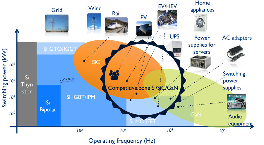 Figure 1: The typical operating frequency and switching power of various semiconductor materials (Source: Yole Group) [see MURA200 for original images]At the same time, the rapid electrification of transport, industry, and energy infrastructure is driving an unprecedented expansion in power conversion applications. This evolution exposes designers to a far wider spectrum of operating conditions.
Critical Challenges in High-Voltage Systems
These evolving expectations place significant stress not only on active devices but also on the passive components integral to these systems. Higher switching speeds, for instance, lead to sharp voltage transients and electromagnetic interference (EMI). Increased voltages impose strict demands on insulation and overall reliability.
Multilayer ceramic capacitors (MLCCs) play a vital role in suppressing high-frequency noise, absorbing transient spikes, and protecting semiconductor devices from overvoltage stress. Therefore, the advancement of MLCCs must align with the increased performance standards required by WBG devices, necessitating enhancements in dielectric compositions and creative packaging approaches.
Taming Transient Spikes
Snubber capacitors are essential in power electronics, especially where high-speed switching induces voltage overshoot and ringing. This is particularly critical during the turn-off transitions of MOSFETs or IGBTs. This issue is heightened in SiC and GaN power semiconductors, which exhibit greater surge voltages compared to traditional silicon IGBTs.
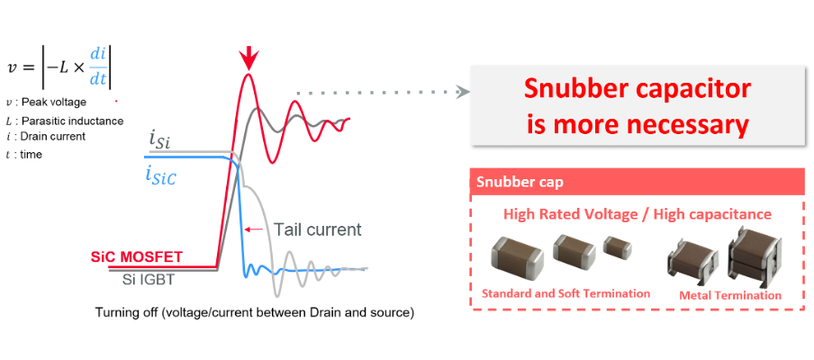 Figure 2: SiC MOSFETs exhibit a higher surge voltage than traditional Si IGBTs (Source: Murata) [see MURA200 for original images]A well-matched snubber capacitor effectively absorbs transient energy, suppresses peak voltages, and damps oscillations. Murata’s metal-termination MLCCs, such as the KC3 and KC9 series, are optimised for use in SiC-based circuits.
The post Powering the Future: How High-Voltage MLCCs Drive Efficiency in Modern Electronics appeared first on ELE Times.
Redefining the human experience with intelligent computing
Courtesy: Qualcomm
Enabling the devices, vehicles and machines that define tomorrow’s world.
What you should know:
- The next UI centres around you, with your AI agent seeing, hearing and acting on your behalf.
- We’re scaling AI to redefine the human experience—powering next-gen wearables and personal AI devices, and driving intelligence into robots, cars and smart homes.
- Our technologies enable extraordinary experiences that consumers and businesses depend on every day—bringing personal and physical AI everywhere.
Think of AI like coffee. You don’t walk into a café and ask for “a beverage brewed from roasted beans” — that’s assumed. You order the experience. Latte, half-pump vanilla, extra shot against a soundtrack of acoustic 90s alternative. The perfect mix to fuel your day, making you more productive, more creative, more you. AI works the same way. It’s a given, not a feature — the foundation of every experience, making each truly yours.
You are at the centre with your agent as your intelligent teammate. This is the next UI. Forget the seemingly endless scrolling and tedious tapping to complete one.single.thing only to do it again.and.again. Instead, your agent moves with you, learns from you and anticipates your needs. And thanks to AI processing on the device, it remains private, contextual and always-on. Like your favourite barista, who knows your order as soon as you walk in, including your (secret) treat every Friday.
We’re leading the charge toward the future of intelligent computing — reimagining possibilities for not only consumers, but also enterprises and industries worldwide. We’re scaling intelligence from edge to cloud, bringing AI everywhere. Our Snapdragon and Qualcomm Dragonwing platforms enable the devices, vehicles and machines that define tomorrow’s world — and redefine the human experience.
And again, I can’t say this enough, it’s all about you. Or more precisely, an “ecosystem of you” where your agent can see, hear and act on your behalf across an emerging category of AI-first intelligent wearables, along with smartphones and AI PCs.
The newest entrant in our Snapdragon X Series Compute Platforms, Snapdragon X2 Plus, delivers agentic AI experiences to aspiring creators, professionals and everyday users — broadening the already-growing Windows PC community.
Your home, too, is transforming into a responsive, intuitive environment. Understanding you and your family, your home adapts to your needs, routines and comforts. Lights, climate, security and entertainment are now intelligent with Dragonwing Q-7790 and Q-8750 processors. The backbone of these AI-enabled experiences and home automation? Connectivity, brought to you by Qualcomm, the leading wireless innovator.
But AI isn’t just personal. It’s also physical, acting alongside you.
Your car is transforming into an adaptive companion, driven by intelligence. Snapdragon is redefining automotive experiences, from enhancing safety and comfort to immersive entertainment. Private, contextual AI — sensing, processing, acting in real time — makes every drive smarter, more efficient and connected.
Advanced autonomous capabilities are also being used to power the next generation of personal service robots, all the way through to industrial full-size humanoids. Thanks to our full-stack robotics system, they will deliver intuitive and impactful assistance with precision, enhancing daily life and industry. And I’m sure they’ll learn how to make your coffee perfectly.
This is truly an exciting time in how technology is evolving around us and for us. Our innovations already power billions of devices, enabling the extraordinary experiences that consumers and businesses depend on every day. And we can’t wait to bring you more.
The post Redefining the human experience with intelligent computing appeared first on ELE Times.
Звіт проректорки з навчальної роботи КПІ Тетяни Желяскової на засіданні Вченої ради 15 грудня 2025 року: "Освіта в КПІ за умов законодавчої трансформації 2025"

Освітня діяльність університету в 2025 році здійснювалася в умовах суттєвої законодавчої трансформації системи вищої освіти, триваючих безпекових викликів та необхідності збереження якості освітнього процесу.
The Forest Listener: Where edge AI meets the wild
Courtesy: Micron
Let’s first discuss the power of enabling. Enabling a wide electronic ecosystem is essential for fostering innovation, scalability and resilience across industries. By supporting diverse hardware, software and connectivity standards, organisations can accelerate product development, reduce costs and enhance user experiences. A broad ecosystem encourages collaboration among manufacturers, developers and service providers, helping to drive interoperability. Enabling an ecosystem for your customers is a huge value for your product in any market, but for a market that spans many applications, it’s paramount for allowing your customers to get to the market quickly. Micron has a diverse set of ecosystem partners for broad applications like microprocessors, including STMicroelectronics (STM). We have collaborated with STM for years, matching our memory solutions to their products. Ultimately, these partnerships empower our mutual businesses to deliver smarter, more connected solutions that meet the evolving needs of consumers and enterprises alike.
The platform and the kit
There’s something uniquely satisfying about peeling back the anti-static bag and revealing the STM32MP257F-DK dev board brimming with potential. As an embedded developer, I am excited when new silicon lands on my desk, especially when it promises to redefine what’s possible at the edge. The STM32MP257F-DK from STMicroelectronics is one of those launches that truly innovates. The STM32MP257F-DK Discovery Kit is a compact, developer-friendly platform designed to bring edge AI to life. And in my case, to the forest. It became the heart of one of my most exciting projects yet: the Forest Listener, a solar-powered, AI-enabled bird-watching companion that blends embedded engineering with natural exploration.
A new kind of birdwatcher
After a few weeks of development and testing, my daughter and I headed into the woods just after sunrise — as usual, binoculars around our necks, a thermos of tea in the backpack and a quiet excitement in the air. But this time, we brought along a new companion. The Forest Listener is a smart birdwatcher, an AI-powered system that sees and hears the forest just like we do. Using a lightweight model trained with STM32’s model zoo, it identifies bird species on the spot. No cloud, no latency, just real-time inference at the edge. My daughter has mounted the device on a tripod, connected the camera and powered it on. The screen lights up. It’s ready! Suddenly, a bird flutters into view. The camera captures the moment. Within milliseconds, the 1.35 TOPS neural processing unit (NPU) kicks in, optimised for object detection. The Cortex-A35 logs the sighting (image, species, timestamp), while the Cortex-M33 manages sensors and power. My daughter, watching on a connected tablet, lights up: “Look, Dad! It found another one!” A Eurasian jay, this time.
Built for the edge … and the outdoors
Later, at home, we scroll through the logs saved on the Memory cards. The system can also upload sightings via Ethernet. She’s now learning names, songs and patterns. It’s a beautiful bridge between nature and curiosity. At the core of this seamless experience is Micron LPDDR4 memory. It delivers the high bandwidth needed for AI inference and multimedia processing, while maintaining ultra-low power consumption, critical for our solar-powered setup. Performance is only part of the story: What truly sets Micron LPDDR4 apart is its long-term reliability and support. Validated by STM for use with the STM32MP257F-DK, this memory is manufactured at Micron’s dedicated longevity fab, ensuring a more stable, multiyear supply chain. That’s a game-changer for developers to build solutions that need to last — not just in home appliances, but in the harsh field environment. Whether you’re deploying an AI app in remote forests, industrial plants or smart homes, you need components that are not only fast and efficient but also built to endure. Micron LPDDR4 is engineered to meet the stringent requirements of embedded and industrial markets, with a commitment to support and availability that gives manufacturers peace of mind.
Beyond bird-watching
The Forest Listener is just one example of what the STM32MP257F-DK and Micron LPDDR4 can enable. In factories, the same edge-AI capabilities can monitor machines, detect anomalies, and reduce downtime. In smart homes, they can power face recognition, voice control and energy monitoring — making homes more intelligent, responsive and private, all without relying on the cloud.
The post The Forest Listener: Where edge AI meets the wild appeared first on ELE Times.
Eddy current in focus: A rapid revisit

Eddy currents are not just textbook curiosities; they are the hidden loops that appear whenever metal meets a changing magnetic field. From DIY levitation tricks to clever braking systems, these swirling paths of electrons keep finding new ways to surprise and inspire.
In this rapid revisit, we will zoom in on the essentials, highlight a few practical pointers, and remind ourselves why this classic effect still merits a place in every innovator’s playbook.
Eddy currents: From losses to brakes to rice cookers
Eddy currents are closed loops of electrical current induced in conductors by a changing magnetic field, as described by Faraday’s law of induction. These currents circulate in planes perpendicular to the applied magnetic field.
By Lenz’s law, eddy currents generate their own magnetic field that opposes the change which created them. This opposition manifests as magnetic drag, joule heating, and energy conversion in conductive materials are exposed to time-varying fields.
The interaction between the applied field and induced currents resists motion. A classic demonstration is a magnet falling slowly through a copper tube—its descent dampened by the opposing magnetic force. As eddy currents circulate, they dissipate energy as heat due to the conductor’s resistance. This loss is problematic in devices such as transformers, motors, and induction coils, where unwanted heating reduces efficiency.
At the same time, eddy currents enable useful applications. In magnetic braking systems, for example, a moving object’s kinetic energy is deliberately converted into heat, providing smooth, contactless deceleration.

Figure 1 A generic eddy current brake is shown with rotor eddy currents resisting motion. Source: Author
Eddy currents embody both challenge and opportunity. In power systems, they waste energy as heat and demand careful design measures such as laminated transformer cores or specialized alloys to minimize losses. Yet the same principle enables precise, contactless control in magnetic braking, induction heating, and nondestructive testing.
Léon Foucault discovered eddy currents in the early 1850s; he also demonstrated Earth’s rotation with the Foucault pendulum. From Foucault’s copper disk to today’s rice cookers and industrial drives, eddy currents illustrate how a single electromagnetic effect can hinder efficiency while powering innovation. Their discovery remains a landmark in the history of electromagnetism.
Eddy currents at work: Quick insights
On paper, eddy currents arise from changing magnetic fields. They form when a conductor moves through a magnetic field or when the field around a stationary conductor varies. In short, any change in the intensity or direction of the magnetic field can drive circulating currents. Their strength scales with the rate of flux change, the loop area, and the field’s orientation, while higher conductor resistivity weakens them.
To grasp how this works, inertia makes a useful analogy. In classical mechanics, a moving body tends to keep moving, while a stationary one stays put. Electromagnetism shows a similar stubbornness: when a conductor encounters a changing magnetic field, it responds by generating an opposing flux through induction. That flux manifests as eddy currents. Picture them as invisible coils forming inside the conductor—the material itself acting like a “built-in electromagnet” that resists change.
A familiar example is the eddy current brake used in heavy vehicles and trains. These auxiliary brakes, often engaged on downhill runs, position electromagnets near a drum on the rotating axle. Once energized, the drum develops eddy currents that push back against the changing flux, creating drag. The beauty of this system lies in non-contact braking—no friction, no wear on drums or pads. Of course, the kinetic energy does not vanish; conservation of energy dictates it reemerges as Joule heating, dissipated as heat in the drum.
The same principle appears in everyday life. Induction cooktops and induction heating (IH) rice cookers rely on high-frequency currents in their coils to generate rapidly changing magnetic fields. These fields drive eddy currents in the conductive pot walls, producing Joule heat that cooks food directly and efficiently.
As a side note, eddy current brakes and electric retarders share the same physics but differ in role. An eddy current brake is a general device found in rail systems, roller coasters, or test rigs, providing smooth, non-contact braking. An eddy current electric/electromagnetic retarder, by contrast, is an auxiliary system integrated into heavy vehicles—buses, trucks, and coaches—to control speed on long descents.
Retarders ease the load on friction brakes, preventing overheating and wear, though they still demand cooling since induced currents generate substantial heat. In short, brakes emphasize stopping power, while retarders emphasize sustained drag torque for safe downhill control.

Figure 2 An electromagnetic retarder mounts mid-shaft and delivers non-contact braking for heavy vehicles. Source: Telma
Harnessing eddy currents in dynamometers
Dynamometers often rely on eddy current action in their background to absorb and measure power. In an eddy current dynamometer, a rotating metallic disc or drum is subjected to a magnetic field; as the engine drives the disc, circulating currents are induced in the metal. These eddy currents create a resistive force proportional to speed, effectively loading the engine while converting mechanical energy into heat.
The dynamometer’s role is to provide a controlled, repeatable load while precisely measuring torque and power, enabling accurate evaluation of engine or motor performance. Their application domain spans automotive testing, industrial machinery evaluation, and research laboratories where reliable power measurement is essential.

Figure 3 An eddy current dynamometer, delivering full power at high rotation speeds, is designed for fast-rotating motors. Source: Magtrol
Eddy current sensors: From magnetic fields to motion insight
An eddy current sensor, often referred to as a gap sensor, operates by generating a high-frequency magnetic field through a coil embedded in the sensor head. When a conductive measuring object approaches this field, eddy currents are induced on its surface, altering the impedance of the sensor coil.
By detecting these impedance changes, the sensor translates variations in transmission length into a precise relationship between displacement and output voltage. Their application fields span precision displacement measurement, vibration monitoring, and shaft run-out detection, with widespread use across the automobile, aerospace, and semiconductor industries.

Figure 4 An industrial-grade contactless proximity sensor measures position by interpreting eddy currents. Source: Messotron
Put another way, the eddy current method employs high-frequency magnetic fields generated by driving an alternating current through the coil in the sensor head. When a metallic target enters this field, electromagnetic induction causes magnetic flux to penetrate the object’s surface, producing circulating eddy currents parallel to that surface. These currents modify the coil’s impedance and eddy current displacement sensors detect the resulting oscillation changes to measure distance.

Figure 5 Drawing illustrates the core mechanism of an eddy current displacement sensor. Source: Author
At this point, it’s important to distinguish between an eddy current probe and an eddy current sensor. The probe is the coil assembly that induces and detects eddy currents, typically used in non-destructive testing (NDT), while the sensor integrates the probe with electronics to deliver calibrated displacement or vibration signals in industrial applications.
Also note that the sensing field of a non-contact sensor’s probe engages the target across a defined area, known as the spot size. For accurate measurement, the target must be larger than this spot size; otherwise, special calibration is required.
Spot size is directly proportional to the probe’s diameter. In eddy-current sensors, the magnetic field fully surrounds the end of the probe, creating a comparatively large sensing field. As a result, the spot size extends to many times the diameter of the probe’s sensing coil.
Wrap-up: Bridging theory and practice in eddy currents
Time for a quick break, yet so many details remain in the fascinating world of eddy currents. I am not covering every nuance here because eddy current methods are broad and specialized, with deeper dives best reserved for dedicated sections. To anchor the essentials: eddy current examination is a nondestructive testing method based on electromagnetic induction.
When applied to detect surface-breaking flaws in components and welds, it’s known as surface eddy current testing. Specially designed probes are used for this inspection, with coils mounted near one end of a plastic housing. During inspection, the technician guides the coil end of the probe across the surface of the component, scanning for variations that reveal discontinuities.
Well, now switch on your eddy current soldering iron—or set up one yourself—and start doing something practical, like building your own probes, sensors, or experimental rigs. Hands-on exploration is the best way to connect theory with practice, and this is the perfect moment to make the leap from reading to making.
For curious makers, eddy current soldering irons are not just another tool, they are a gateway into experimenting with induction heating itself. A coil generates a rapidly changing magnetic field, inducing circulating currents in the conductive tip or sleeve. These eddy currents encounter resistance and dissipate energy as heat, delivering rapid warm-up and stable temperature exactly where it is needed.
Whether you pick up a ready-made station or build a DIY rig, you will be blending theory with practice in the most tangible way. It’s a perfect project to showcase how electromagnetic principles—Faraday’s law and Lenz’s law in action—can power real-world innovation.
 T. K. Hareendran is a self-taught electronics enthusiast with a strong passion for innovative circuit design and hands-on technology. He develops both experimental and practical electronic projects, documenting and sharing his work to support fellow tinkerers and learners. Beyond the workbench, he dedicates time to technical writing and hardware evaluations to contribute meaningfully to the maker community.
Related Content
- Maxon: Inductive encoder is based on eddy currents
- The difference between inductive proximity, displacement, and eddy-current sensors
The post Eddy current in focus: A rapid revisit appeared first on EDN.
Nitride Global, USLLC and Axiom Space awarded NASA SBIR grant
Wolfspeed’s soft demand for EV application offset by 50% quarterly revenue growth for AI data-center application
Solution Suite Concept: Software-Based Refrigerator
Courtesy: Renesas
Imagine a world without cold storage—medicines would spoil, food would perish, and supply chains would collapse. Refrigeration systems are vital to modern life, from pharmaceutical coolers to large-scale warehouses. These systems form the backbone of the cold chain, ensuring products meet strict storage requirements.
To achieve durability and sustainability in these operations, embracing AI is essential for maximum performance optimisation. Renesas has been continuously innovating in this space, delivering a range of AI-driven solutions tailored for the refrigeration industry—helping businesses enhance efficiency, reliability, and energy savings.
Renesas Enablement for AI-powered Refrigeration Solutions
Renesas’ solution concept introduces a suite of AI-driven applications designed to tackle everyday challenges in refrigeration systems. These proposals focus on enhancing operational efficiency and reliability in key areas such as predictive maintenance, energy optimisation, and asset management, among others.
Refrigerant gas is crucial for maintaining stable cold temperatures in cooling systems. Over time, however, leaks can develop due to wear and tear in pipes or refrigerant circuits. To address this challenge, Renesas AI leverages advanced AI algorithms to detect anomalies by analysing changes in electrical current and compressor vibrations. This proactive approach enables timely maintenance, prevents costly breakdowns, and ensures optimal cooling efficiency.
Compressor Overheat Detection
Compressor overheating can result from issues such as low refrigerant levels or clogged filters, leading to potential system damage. Renesas AI HVAC solutions go beyond leak detection by continuously monitoring filter conditions and measuring intake airflow in real time. By analysing this data, the system predicts risks before they escalate, ensuring the cooling system operates efficiently and reliably.
Cooling Capacity Monitoring
Renesas HVAC solutions integrate advanced AI features to predict fan imbalances that directly impact cooling efficiency. Using AI models trained with electrical current data, these anomalies can be detected, enabling seamless and sensorless monitoring. This proactive approach enhances system reliability and ensures optimal cooling performance.
Assets Monitoring: Availability and Expiry Tracking
AI-powered object detection and classification enable real-time monitoring of stock levels and refrigerated assets. The system can automatically suggest restocking needs and estimate lead times for each item. Reducing the need for manual inventory checks and minimising the frequency of opening cooling units, it reduces energy consumption and improves operational efficiency.
Person Identification
AI-powered person identification enhances security and user experience in refrigeration systems. Authorised access can be ensured through two approaches:
- Vision-based authentication using an object detection model combined with on-device learning for custom face recognition.
- Voice-based authentication using a speaker identification model with a microphone sensor.
These methods can be combined for two-step authentication, which is especially critical in medical or industrial refrigeration environments. For home appliances, person identification enables context-aware interactions, such as personalised dietary recommendations or recipe suggestions, creating a smarter and more intuitive user experience.
By integrating real-time monitoring, predictive maintenance, and intelligent object detection, these systems deliver optimal performance, energy efficiency, and operational reliability. From detecting refrigerant leaks and airflow issues to predicting fan imbalances and automating inventory management, the Renesas solution concept offers a comprehensive, end-to-end approach to cooling system optimisation.
This seamless and sensorless monitoring capability not only extends system longevity but also drives significant energy savings. As demand for smarter, more efficient refrigeration systems grows, Renesas is leading the way, pioneering the next generation of intelligent cooling solutions.
The post Solution Suite Concept: Software-Based Refrigerator appeared first on ELE Times.
The V2X Revolution: Satellite Integration, Quantum Security, and 5G RedCap Reshape Automotive Connectivity
Imagine your car negotiating traffic with satellites, quantum-encrypted handshakes, and roadside infrastructure—all while you sip your morning coffee. This isn’t science fiction; it’s the V2X revolution unfolding in production vehicles by 2027. As the Vehicle-to-Everything market hurtles from $6.53 billion in 2024 toward a staggering $70.94 billion by 2032, three converging technologies are rewriting the rules of automotive connectivity: satellite-integrated networks that promise coverage where cell towers fear to tread, post-quantum cryptography racing against the quantum computing threat, and cost-optimised 5G RedCap systems making autonomous driving infrastructure economically viable. The question isn’t whether your next vehicle will be connected—it’s whether the ecosystem will be ready when it rolls off the line.
The Convergence Catalyst: When Satellites, Quantum, and RedCap Collide
The automotive industry has weathered countless transformations, but the V2X revolution of 2025-2026 represents something unprecedented: three disparate technologies—satellite connectivity, quantum cryptography, and 5G RedCap, converging into a single automotive imperative as the market accelerates toward $70.94 billion by 2032.
The strategic calculus facing OEMs isn’t simply about adopting V2X; it’s about choosing which technological bet defines their competitive position. Some prioritise satellite-integrated Non-Terrestrial Networks, banking on 5GAA’s 2025 demonstrations proving vehicles can maintain emergency connectivity where terrestrial infrastructure fails. Their roadmaps target 2027 commercial deployments, envisioning truly ubiquitous vehicle connectivity from urban centres to remote highways.
“Connectivity is becoming more and more important for vehicles. No connection is not an option. Satellite came to our attention 3 to 5 years ago, and then it was costly and proprietary with large terminals,” said Olaf Eckart, Senior Expert, Cooperations R&D / Engineering Lead, NTN, BMW
Others race against the quantum threat timeline. With NIST finalising quantum-resistant standards including CRYSTALS-Kyber and CRYSTALS-Dilithium, these companies face an uncomfortable truth: today’s vehicle encryption could be obsolete within a decade. Their 18-24 month roadmaps aren’t about adding features; they’re about future-proofing against a cryptographic paradigm shift most consumers don’t yet understand.
The pragmatist camp focuses on 3GPP Release 17’s RedCap specifications entering mass production. These organisations see cost-effective 5G variants as critical enablers for vehicle-road-cloud integration architectures, making L2+ autonomous driving economically viable at scale.
What’s remarkable isn’t the diversity of approaches; it’s that all three are simultaneously correct. The V2X ecosystem emerging in 2026-2027 won’t be defined by a single winner but by seamless integration of all three domains. Vehicles rolling off 2027 production lines will need satellite backup for coverage gaps, quantum-resistant security for longevity, and RedCap efficiency for cost-effectiveness.
The question keeping executives awake isn’t which technology to choose; it’s whether their organisations can master all three fast enough to remain relevant.
Engineering Reality Check: Breaking Through the Technical Bottlenecks
Every breakthrough technology comes with footnotes written in engineering challenges, and V2X is no exception. The gap between demonstrations and production-ready systems is measured in thousands of testing hours and occasional failures that never reach press releases.
Consider satellite-integrated V2X’s deceptively simple promise: connectivity everywhere. Reality involves achieving seamless terrestrial-to-Non-Terrestrial Network handovers while maintaining sub-100ms latency that safety-critical applications demand. When vehicles at highway speeds switch from cellular towers to LEO satellite constellations, handovers must be invisible and instantaneous. Engineers are discovering that 3GPP Release 17/18 standards provide frameworks, but real-world implementation requires solving synchronisation challenges that textbooks barely address.
Post-quantum cryptography presents an even thornier dilemma. CRYSTALS-Kyber and CRYSTALS-Dilithium aren’t just longer keys—they’re fundamentally different mathematical operations consuming significantly more processing power than today’s RSA or ECC algorithms. Automotive-grade ECUs, designed with tight power budgets and cost constraints, weren’t built for quantum-resistant workloads. Development teams wrestle with a trilemma: maintain security standards, meet latency requirements, or stay within thermal envelopes. Pick two.
The integration paradox compounds complexity. Can existing vehicles receive V2X capabilities through OTA updates and modular hardware? Sometimes, a 2024 model with appropriate sensor suites might support RedCap upgrades via software. But satellite antenna arrays and quantum-capable security modules often require architectural changes that can’t be retrofitted; they need initial platform integration.
The coexistence problem adds another layer. Many vehicles must support multiple V2X standards simultaneously: legacy DSRC, C-V2X, and emerging satellite connectivity. Ensuring these systems don’t interfere while sharing antenna space and processing resources is creative problem-solving happening in testing facilities at 3 AM.
What separates vapourware from production-ready solutions isn’t the absence of challenges; it’s how engineering teams respond when elegant theory collides with messy reality.
NXP’s Post Quantum Cryptography chips use on-chip isolation so that “in the event of an identified attack, the technology doesn’t let the attack spread to other chips and controllers in the vehicle,” said the NXP Semiconductors, Engineering Team, Marius Rotaru (Software Architect) & Joppe Bos (Senior Principal Cryptographer).
Beyond the Vehicle: Infrastructure, Ecosystems, and the Path to Scale
The most sophisticated V2X technology becomes an expensive paperweight without supporting ecosystems. This truth is reshaping automotive development models, forcing OEMs beyond the vehicle into infrastructure challenges they’ve historically ignored.
The infrastructure gap is staggering. Satellite-integrated V2X requires ground stations for orbit tracking and handover coordination. Post-quantum security needs certificate authorities upgraded with quantum-resistant algorithms across entire PKI hierarchies. RedCap-enabled vehicle-road-cloud architectures demand roadside units at sufficient density, plus edge computing infrastructure processing terabytes of sensor data with minimal latency.
No single company can build this alone, spawning partnership models from traditional supplier relationships into complex consortia. Automotive OEMs partner with telecom operators on spectrum allocation, governments on roadside infrastructure and regulatory frameworks, and satellite operators, cloud providers, and cybersecurity firms; often simultaneously, sometimes competitively.
Regulatory landscapes add complexity. V2X touches spectrum allocation, data privacy, cybersecurity standards, and safety certification, each governed by different agencies with different timelines. Europe swung toward C-V2X after years of DSRC mandates. China receives state-backed vehicle-road-cloud infrastructure investment. United States approaches vary by state, creating fragmented deployment landscapes complicating nationwide rollouts.
When does this reach mainstream production? RedCap systems enter vehicles now, in 2025-2026, leveraging existing cellular infrastructure. Satellite integration likely reaches commercial deployment by 2027-2028 for premium vehicles and emergency services. Post-quantum security faces longer timelines; threats aren’t imminent enough to justify computational overhead across fleets.
Three factors will accelerate or delay timelines: infrastructure deployment speed, regulatory harmonisation, and killer applications making V2X tangible to consumers. V2X reaches mainstream adoption when it solves problems people actually have.
Looking toward 2027-2030, the competitive landscape splits between integrated mobility providers mastering the full vehicle-infrastructure-cloud stack and specialised component suppliers. Winners will be organisations that built ecosystems delivering end-to-end experiences. In the V2X era, the vehicle is just the beginning.
by: Shreya Bansal, Sub-Editor
The post The V2X Revolution: Satellite Integration, Quantum Security, and 5G RedCap Reshape Automotive Connectivity appeared first on ELE Times.
Building a programmable DC-DC Power Supply with I2C Interface (I2C-PPS). Part 1 - Idea
. Part 1 - Idea") | I was lurking through DigiKey catalog and found a TI buck-boost controller with I²C interface - BQ25758S. The controller allows to create a programmable power supply with quite impressive output specs - voltage 3.3-26V and current up to 20A. Decided to give it a try and create a compact board for my RPI Zero. I don't think I'll go above 3A input (which means only 500mA@26V give or take some efficiency) and it's a bit of a shame that the controller doesn't go below 3.3V (much better would be at least 1.8V). For starter created an umbrella repository - github.com/condevtion/i2c-pps. Any "well, actually" are very welcome! [link] [comments] |
My first project: Universal Traction Control System for Motorcycles!!
 | I really like motorcycles, specially old sports bikes, but, they do come with a terrible thing, they don't have any safety electronics at all, ABS, TCS, nothing, completely barebones, and I consider myself a pretty new rider, so I'm starting a project where I'm gonna make my own traction control, using hall effect sensors and laser cut tone wheels for sensing both of the wheels rotation, so the ESP32 inside the main PCB can do the math, alongside the MPU6050 GY-512, so it correct the "slipage rate" as the bike inclines from side to side into turns in the twisties, it's definitely not gonna be perfect from the get go, but I'm really hopeful that this thing can work properly. If you're wondering, they don't act directly on the brakes, but rather using the relay to shut off the ignition coil for a few microseconds as the bikes takes grip again, hopefully this will be able to help both me and several other riders ride their dream bikes more safely! Everything is at a very starting phase, but I did already order all the PCBs from JLCPCB and the components I bought locally, so excited to see how it turns out! [link] [comments] |
Modifying the INA226 Current Sensor for High-Power Applications
 | I’d like to share my experience building a "rough gauge" for my LiFePO4 battery pack. Instead of using an off-the-shelf Smart BMS, I chose the DIY route to better understand the underlying physics and processes. Stock INA226 modules come with a 100 mΩ shunt resistor, which limits the current measurement to a measly 800 mA. This is far too low for a power battery.
To find the exact resistance value, I ran a series of tests and compared the readings with a UNI-T UT61 multi meter. The calculated precision value is 4.392 mΩ.
The biggest challenge is heat. At currents above 10 A, the shunt begins to warm up noticeably. This creates Therm-EMF (the Seebeck effect), which causes "phantom" readings of about 50 mA on the screen for several minutes after the load is disconnected, until the node cools down. More details here: https://en.neonhero.dev/2026/02/modifying-ina226-from-08a-to-high-power.html [link] [comments] |
Test if the diodes work (Silly power supply for a lone lamp update)
") | A long anticipated update for "Silly power supply for a lone lamp" post :) The original post showed a simple set of low power batteries connected in parallel supplying a 12V/50mA lamp. The schematic featured a diode per battery to prevent them from feeding each other. Here, I decided to check experimentally if the diodes indeed work as expected. I used an STM32F103 module as multichannel ADC, a set of resistors to scale down from 0-18V to 0-3V and a RPi Zero 2W as a 5V power supply and to collect data. Potentiometers were set to 20k creating 6 100k/20k voltage dividers (pic 3). First, measured lamp and batteries voltages with a fresh set batteries. They held around 3 hours 45 minutes. The set had voltage around 12.6V fresh without load. Upon switching on the load they immediately dropped to 12V and then spent most of the time going from 10.5 to 8.5V as the pic 4 shows. The diodes took about 350mV so lamp's voltage went clearly below batteries. Then I mixed 3 fresh and 3 used batteries and actually was really surprised with how clearly it showed when used batteries kicked in. The last pic shows voltage drop across diodes and comparing with the previous one you can see that the diodes for used batteries open as voltage reaches around 200mV. Which is a great real-world demo of how low is cut-in (or knee) voltage for a Schottky diode can be (here SD103A used). [link] [comments] |
I hear we like to sort stuff here? How about a gallon of resistance?
 | submitted by /u/mofomeat [link] [comments] |
Weekly discussion, complaint, and rant thread
Open to anything, including discussions, complaints, and rants.
Sub rules do not apply, so don't bother reporting incivility, off-topic, or spam.
Reddit-wide rules do apply.
To see the newest posts, sort the comments by "new" (instead of "best" or "top").
[link] [comments]
Pages


![[link]](https://i.redd.it/sv5sdo2z1sjg1.png)
![[link]](https://i.redd.it/v6u4b0ql4kjg1.jpeg)