
Feed aggregator
PLC, PAC, and Industrial PC Architectures for Automation
Introduction
Industrial automation is undergoing a fundamental transformation. Traditional control systems designed primarily for machine sequencing and process control are now expected to support advanced analytics, predictive maintenance, artificial intelligence (AI), digital twins, cloud connectivity, and cybersecurity frameworks. As manufacturing and infrastructure systems become increasingly data-intensive, engineers face a critical challenge: selecting the most appropriate control architecture.
For decades, the Programmable Logic Controller (PLC) was the undisputed backbone of industrial automation. Later, Programmable Automation Controllers (PACs) emerged to bridge the gap between deterministic control and information processing. Today, Industrial PCs (IPCs) have evolved into powerful edge-computing platforms capable of running sophisticated automation software alongside AI and data analytics workloads.
The boundaries between these technologies are becoming increasingly blurred. Modern PLCs offer edge computing capabilities, PACs provide PC-like processing power, and industrial PCs deliver real-time deterministic control. Consequently, selecting the right controller is no longer about choosing the “best” technology but about understanding engineering requirements, operational constraints, and lifecycle considerations.
Understanding the Architectural Differences
PLC: The Deterministic Workhorse
PLCs were designed specifically for industrial environments where reliability and deterministic operation are paramount. Their architecture is optimized for real-time control tasks, including discrete I/O management, sequencing, interlocking, and safety functions.
Typical PLC architecture includes:
- Dedicated real-time operating systems
- Ruggedized hardware
- Scan-cycle execution model
- Integrated digital and analog I/O
- Long operational life cycles
- High resistance to electrical noise and harsh environments
The PLC continuously executes a control loop consisting of:
- Input scan
- Logic execution
- Output update
- Communication services
This deterministic behavior makes PLCs ideal for packaging machines, conveyor systems, assembly lines, water treatment plants, and utility infrastructure.
Key Strength: Predictable control performance with extremely high reliability.
Limitation: Limited computational capability for data-intensive applications.
PAC: Bridging Control and Information
Programmable Automation Controllers emerged as industrial systems became more complex and interconnected.
PACs combine the deterministic nature of PLCs with the flexibility of modern computing platforms. Unlike traditional PLCs, PACs support:
- Multi-domain automation
- Advanced motion control
- Large memory capacity
- Object-oriented programming
- Integrated networking
- Database connectivity
PACs generally comply with IEC 61131-3 standards while supporting higher-level software architectures.
Industrial PC: The Data-Centric Controller
Industrial PCs bring standard computing power into the industrial environment.
Modern IPCs feature:
- Multi-core processors
- High-capacity memory
- Solid-state storage
- Virtualization support
- AI acceleration
- GPU integration
- Industrial communication interfaces
Unlike PLCs, IPCs typically run:
- Windows
- Linux
- Real-Time Linux
- Hypervisor-based architectures
The rise of Industry 4.0 has significantly increased IPC adoption because they can process massive datasets locally while maintaining cloud connectivity.
Engineering Decision Framework
Instead of asking, “Which controller is better?” engineers should ask the following questions:
- How Critical Is Deterministic Performance?
Applications such as:
- Emergency shutdown systems
- Turbine control
- Motion synchronization
- Safety systems
require guaranteed response times.
In such cases, PLCs and PACs remain the preferred solutions.
- How Much Data Must Be Processed?
Modern smart factories generate terabytes of operational data.
Applications involving:
- AI-based inspection
- Video analytics
- Condition monitoring
- Predictive maintenance
often exceed traditional PLC capabilities and favour Industrial PCs.
- What Is the Environmental Requirement?
PLCs generally provide the highest environmental resilience, although ruggedized IPCs continue to improve.
- What Is the Expected Lifecycle?
Many manufacturing facilities expect automation assets to operate for decades.
PLC vendors often provide long-term support and product availability, making them attractive for infrastructure projects with extended service lives.
Industrial PCs may require more frequent hardware refresh cycles.
- What Are the Cybersecurity Requirements?
As operational technology (OT) becomes connected to enterprise IT networks, cybersecurity has become a critical design consideration.
Industrial PCs running conventional operating systems introduce a larger attack surface than dedicated PLC platforms.
Engineers must evaluate:
- Patch management
- Network segmentation
- Secure boot
- Endpoint protection
- Zero-trust architectures
before selecting a controller platform.
Emerging Hybrid Architectures
The most significant trend in industrial automation is convergence.
Leading automation vendors are increasingly integrating PLC, PAC, and IPC technologies into unified architectures.
Companies such as Siemens, Rockwell Automation, Schneider Electric, Beckhoff Automation, and Bosch Rexroth are investing heavily in software-centric automation architectures that blur traditional controller boundaries.
In many modern facilities, the architecture is no longer PLC versus IPC. Instead, PLCs provide deterministic machine control while Industrial PCs handle AI, visualization, and analytics at the edge. PACs often serve as the integration layer between these domains.
The Future: Software-Defined Industrial Control
The next generation of automation systems will increasingly separate software from hardware.
Virtualized controllers running on industrial servers are beginning to challenge conventional hardware-based automation architectures. AI-assisted engineering tools, digital twins, and edge computing platforms will continue driving demand for more computationally capable control systems.
However, deterministic control remains the foundation of industrial automation. Regardless of future innovations, the engineering challenge will continue to revolve around balancing reliability, performance, security, scalability, and cost.
Conclusion
The debate between PLCs, PACs, and Industrial PCs is no longer a simple technology comparison. Each architecture serves a distinct purpose within modern automation ecosystems.
For today’s engineers, the optimal solution is increasingly a hybrid architecture that combines the strengths of all three platforms. Success lies not in choosing a single controller type but in understanding the specific operational requirements and designing a system architecture that balances control integrity with digital innovation.
As factories evolve toward autonomous, connected, and intelligent operations, the future belongs to architectures that seamlessly integrate deterministic control with data-driven intelligence.
The post PLC, PAC, and Industrial PC Architectures for Automation appeared first on ELE Times.
Optics and Silicon Photonics: The Next Data Highway Inside Chips
For more than five decades, the semiconductor industry has relied on a simple principle: increasing transistor density to deliver higher computing performance. While transistor scaling continues to advance, a new bottleneck has emerged inside modern computing systems—data movement.
Today’s processors, AI accelerators, memory systems, and data centers spend a significant portion of their energy simply moving data through metallic interconnects. Traditional copper wiring, which has served electronics faithfully for decades, is rapidly approaching its physical limitations. Resistance, capacitance, signal attenuation, electromagnetic interference, and heat generation increasingly constrain performance.
To overcome these challenges, the semiconductor industry is turning toward a revolutionary solution: Silicon Photonics. Instead of electrons traveling through copper traces, future chips will increasingly use photons—particles of light—to carry information. The result could be processors capable of transferring data at unprecedented speeds while consuming significantly less power and generating far less heat.
What is Silicon Photonics?: Silicon Photonics is a technology that integrates optical communication components directly onto silicon chips using semiconductor manufacturing processes similar to those used for CMOS integrated circuits.
Instead of transmitting information via electrical signals, silicon photonic devices use light waves traveling through microscopic optical waveguides fabricated on silicon wafers.
A typical silicon photonic system consists of:
- Lasers
- Optical modulators
- Waveguides
- Multiplexers
- Photodetectors
- Electronic control circuits
Together, these components allow information to be converted from electrical signals into optical signals and back again.
For working engineers, the story is no longer just about making transistors smaller. It is about moving data fast enough to keep up with them. As electrical links stretch across boards, packages, and racks, copper starts to run into familiar physical problems: resistance, crosstalk, signal loss, heat, and rising power cost per bit. Silicon photonics answers that bottleneck by carrying information as light rather than electrons, using optical links to push bandwidth higher while reducing the energy spent on interconnects. In practice, that makes photonics one of the most important enabling technologies for AI systems, HPC clusters, and data-center networking.
The engineering shift is straightforward in concept and hard in implementation. A silicon photonics platform integrates optical devices with standard CMOS-style manufacturing so data can be modulated, routed, and detected on or near the chip package. Intel describes its platform as combining silicon manufacturing scale with light on a single chip, and says its solutions now span 400G, 800G, and 1.6T-class interfaces. Ayar Labs takes a similar direction with optical I/O chiplets, positioning them as a low-power, low-latency alternative to copper backplanes and pluggable optics.
The practical reason this matters is bandwidth density. When systems scale from a handful of accelerators to dense AI fabrics, the bottleneck is often not compute silicon itself but how quickly data can enter, leave, and circulate around it. That is why the industry is moving from pluggable transceivers toward co-packaged optics, where optical engines sit much closer to the switch ASIC or accelerator package. NVIDIA says its silicon-photonics-based networking is aimed at this problem, with its 2025 Spectrum-X Photonics announcement targeting scale-out AI factories and claiming major gains in energy efficiency and resiliency. Broadcom is also pushing co-packaged optics and silicon-photonics chiplets for high-radix AI networks.
A useful way to think about the transition is this: copper is still excellent for short, simple, low-cost links, but it becomes expensive in power and signal integrity as reach and rate increase. Silicon photonics does not eliminate that tradeoff everywhere, but it moves the break-even point dramatically. Intel says its platform has already shipped more than 8 million photonic integrated circuits and more than 32 million on-chip lasers, while NVIDIA and Broadcom are both anchoring their latest AI networking roadmaps around photonics and co-packaged optics.
For engineers, the opportunity is not just faster links; it is system design freedom. Optical interconnects can relax board routing constraints, reduce electrical retiming overhead, and help keep power budgets under control as data rates climb. That is why the near-term adoption path is strongest in the I/O layer, package-to-package links, switch fabrics, and rack-scale interconnects, where the cost of moving bits is becoming as important as the cost of computing them. The architecture of future systems will still be electronic at the logic core, but increasingly optical at the boundaries where data movement hurts most.
In short, silicon photonics is not a futuristic side project anymore. It is becoming a serious engineering answer to a very present problem: how to keep AI, HPC, and networking systems from drowning in their own data traffic. The companies most visibly shaping the field today include Intel, NVIDIA, Ayar Labs, and Broadcom, each attacking the same bottleneck from a slightly different angle. For engineers building the next generation of systems, photonics is moving from “interesting” to “necessary.”
The semiconductor industry’s next breakthrough may not come solely from smaller transistors, but from replacing electrons with photons for data movement. As copper interconnects approach fundamental physical limits, silicon photonics offers a path toward dramatically higher bandwidth, lower latency, and significantly improved energy efficiency.
For working engineers, the transition to photonic computing represents more than an incremental improvement—it signals a fundamental architectural shift in how information is transported within and between computing systems. Companies such as Intel, NVIDIA, Cisco, Broadcom, Ayar Labs, Lightmatter, and Celestial AI are already laying the foundation for this future.
Over the coming decade, optical interconnects, co-packaged optics, and photonic processors are expected to become core enabling technologies for AI supercomputers, hyperscale data centers, and next-generation embedded systems. Just as silicon transformed computing in the twentieth century, silicon photonics may define the computational infrastructure of the twenty-first century.
The post Optics and Silicon Photonics: The Next Data Highway Inside Chips appeared first on ELE Times.
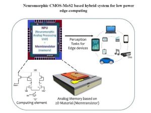
Neuromorphic Engineering & Edge AI: The Future of Intelligent Computing
Artificial Intelligence is rapidly transforming industries, but traditional AI systems come with a major challenge: enormous energy consumption. Most modern AI applications depend on cloud-based data centers packed with power-hungry GPUs and servers. As billions of smart devices become connected, this centralized approach is becoming increasingly expensive, slower, and environmentally unsustainable.
A revolutionary solution is emerging through Neuromorphic Engineering and Edge AI. Instead of relying entirely on distant cloud servers, scientists and engineers are building specialized chips that mimic the structure and behavior of the human brain. These advanced processors, known as neuromorphic chips and AI accelerators, process information directly on devices such as smartphones, drones, medical wearables, robots, and autonomous vehicles. This approach dramatically reduces latency, improves privacy, and cuts energy consumption.
What is Neuromorphic Engineering?
Neuromorphic engineering is a field that designs computer hardware inspired by biological neural systems. Traditional computers process data sequentially and continuously, even when there is little meaningful activity. The human brain, however, operates differently. Neurons only “fire” when necessary, making the brain remarkably energy efficient while handling complex sensory information in real time.
Neuromorphic chips attempt to replicate this behavior using Spiking Neural Networks (SNNs). Unlike conventional neural networks that constantly process streams of data, SNNs activate only when changes occur. This event-driven architecture significantly reduces unnecessary computation and power usage.
Brain-Inspired AI Hardware
Modern neuromorphic processors integrate memory and computing together instead of separating them like traditional CPU and GPU architectures. This eliminates the “von Neumann bottleneck,” where large amounts of energy are wasted transferring data between memory and processors.
Companies and research institutions worldwide are developing advanced neuromorphic systems. Intel’s Loihi 2 chip, for example, can simulate millions of neurons while consuming only a fraction of the energy used by traditional AI hardware. Some experimental chips operate in milliwatts rather than watts, making them ideal for portable and battery-powered devices.
Researchers are also exploring technologies such as memristors, which combine memory and processing in a single component, closely resembling biological synapses. These innovations could eventually enable AI systems that learn continuously and adapt in real time without relying on cloud computing.
The Rise of Edge AI
Edge AI refers to running artificial intelligence directly on local devices rather than sending data to centralized servers. Today, many AI applications depend on cloud infrastructure, which introduces delays and requires constant internet connectivity. Edge AI changes this model by bringing intelligence closer to the source of data.
For example:
- Self-driving cars must make decisions instantly without waiting for cloud responses.
- Smart surveillance cameras need real-time object recognition.
- Wearable healthcare devices must continuously monitor vital signs with minimal battery drain.
- Industrial robots require rapid reactions in manufacturing environments.
Neuromorphic processors are particularly well-suited for these applications because they deliver near-zero latency and ultra-low power consumption.
Energy Efficiency and Sustainability
One of the biggest advantages of neuromorphic computing is energy efficiency. Conventional AI training and inference systems consume massive amounts of electricity. Data centers supporting generative AI models now require enormous cooling systems and power grids. Neuromorphic systems dramatically reduce this burden. According to recent studies, some neuromorphic architectures can achieve over 100 times better energy efficiency compared to traditional deep learning hardware.
The human brain itself consumes only about 20 watts of power — less than a dim light bulb — while performing tasks that remain challenging for modern computers. Neuromorphic engineers aim to approach this extraordinary level of efficiency. This has major implications for sustainable computing. As global AI adoption accelerates, reducing energy demand will become essential for lowering operational costs and minimizing environmental impact.
Real-World Applications
Neuromorphic Edge AI is already finding applications across multiple industries:
Healthcare
Wearable devices powered by neuromorphic chips can continuously monitor patient conditions, detect abnormalities, and even predict medical emergencies with minimal battery usage.
Autonomous Vehicles
Self-driving systems require split-second decisions. Neuromorphic processors enable rapid sensor processing for safer navigation and collision avoidance.
Robotics
Robots equipped with brain-inspired AI can react more naturally to changing environments while consuming far less energy.
Defense and Aerospace
Low-power edge computing is critical for drones, radar systems, and satellites operating in remote environments.
Consumer Electronics
Future smartphones, AR glasses, and smart home devices may run advanced AI locally without depending heavily on cloud services.
Challenges Ahead
Despite its promise, neuromorphic computing is still in its early stages. Developing efficient training methods for spiking neural networks remains difficult, and software ecosystems are less mature than traditional AI frameworks. Manufacturing specialized hardware at scale is another challenge. However, rapid advances in semiconductor technology and growing demand for sustainable AI are accelerating innovation in this field.
Conclusion
Neuromorphic Engineering and Edge AI represent a major shift in the future of computing. By mimicking the brain’s architecture, these technologies enable intelligent devices that are faster, smarter, and far more energy efficient than traditional systems. As AI continues to expand into every aspect of daily life, neuromorphic chips could become the foundation for a new generation of sustainable, low-latency, and autonomous technologies. The future of AI may no longer reside solely in giant cloud data centers — it may live directly inside the devices we use every day.
The post Neuromorphic Engineering & Edge AI: The Future of Intelligent Computing appeared first on ELE Times.
Ensuring Reliable AI in Safety-Critical Systems: Challenges and Engineering Solutions
In safety-critical environments, reliability is paramount, and errors have immediate, real-world consequences. If an autonomous system falters in urgent decisions, a clinical support tool misguides diagnoses, or an industrial controller fails in hazardous conditions, the results can be life-threatening. Artificial intelligence must be unwaveringly accurate and reliable at every moment to ensure safety and maintain trust in deployment.
This demands a fundamental shift in AI system engineering. Unlike traditional domains, where model accuracy or benchmark performance may suffice, safety-critical applications require predictable, consistent, and fail-aware behaviour across diverse conditions. The real challenge is to establish AI as fundamentally trustworthy in situations where failure is not an option, making reliability, not just intelligence, the core success criterion.
As AI integrates into mission-critical infrastructure, reliability is not just a technical requirement; it is the foundation and defining goal for deploying AI in safety-critical systems.
The Reliability Gap: From Probabilistic Models to Deterministic ExpectationsA core engineering challenge now demands urgent attention: a deep mismatch exists between traditional system design and modern AI behaviour. Safety-critical systems have historically been deterministic, producing predictable and verifiable outputs. In stark contrast, AI models are inherently probabilistically trained on data, influenced by variability, and alarmingly sensitive to environmental changes.
This mismatch creates a reliability gap that cannot be ignored in high-stakes deployments:
- High accuracy does not ensure safe behaviour in rare or unseen scenarios
- Models may generate confident yet incorrect predictions
- Behaviour under edge conditions remains difficult to anticipate
In safety-critical contexts, such uncertainties quickly become intolerable. Systems must now be engineered not just for performance, but for rigorous assurance under uncertainty. As Sundar Pichai warned, “The more capable AI becomes, the more critical it is to ensure it behaves safely and predictably.” This is no longer a theoretical challenge; it is the defining engineering crisis of our time.
Core Challenges in Deploying Reliable AI SystemsThe dynamic nature of real-world environments directly undermines reliability. AI systems trained in controlled settings inevitably confront distribution shifts at deployment scenarios absent from training data. These shifts degrade performance, especially in rare or safety-critical contexts.
In addition to distribution shifts, another critical issue is the inability of many models to communicate uncertainty. AI systems often produce outputs with high confidence, even when operating outside their domain of competence. In applications involving autonomous control or real-time decision-making, such overconfidence can lead to unsafe outcomes without warning.
Building on the previous concern, explainability is equally important. Safety-critical systems demand traceability and accountability, yet many AI models function as opaque decision-makers. Without the ability to interpret decisions, validating system behaviour and meeting regulatory expectations becomes significantly more difficult.
Finally, AI systems do not operate in isolation. They are part of a broader ecosystem involving sensors, embedded hardware, and control systems. Variability at any of these levels, whether due to sensor noise, latency, or hardware constraints, can influence overall system reliability. Ensuring dependable operation, therefore, requires a holistic, system-level perspective.
When AI Fails: Understanding System-Level RiskFailures in safety-critical AI systems are rarely isolated events. A single incorrect output can propagate across the system, leading to cascading effects that compromise overall functionality.
The most critical risks include:
- Silent failures, where incorrect outputs remain undetected
- Error propagation across interconnected system components
- Over-reliance on AI outputs, reducing effective human oversight
These risks highlight a key engineering principle: reliability must be designed into the system from the outset. It cannot be treated as a post-deployment evaluation metric.
Engineering Reliable AI: From Models to SystemsWe must shift from model-centric development to system-level assurance to address these challenges. We need to embed reliability across the entire lifecycle, from data collection to deployment and monitoring.
A foundational step is robust data engineering. Expand datasets to capture real-world variability. Simulate edge-case scenarios. Continuously monitor for data drift. These approaches improve generalisation and reduce unexpected system behaviour.
Equally important is uncertainty-aware system development. Integrate mechanisms that estimate prediction confidence so that models detect when they exceed their limits. This enables fallback strategies, like deferring to human operators or switching to safe modes. In this way, AI evolves from static prediction to self-aware system components.
Validation methodologies must also evolve. Traditional testing approaches are insufficient for capturing the complexity of AI behaviour. Scenario-based testing, simulation of rare or hazardous conditions, and stress testing under extreme inputs are becoming essential tools for evaluating reliability beyond standard datasets.
Explainability strengthens system assurance. While full transparency is rare, interpretable insights enable debugging, validation, and regulatory compliance. These capabilities help build trust among stakeholders.
Redundancy plays a central role in ensuring reliability. Instead of relying on a single model, systems increasingly incorporate multiple validation layers, hybrid architectures combining AI with rule-based logic, and predefined fail-safe states. As Satya Nadella emphasises, “Trust must be built into every layer of AI systems.” Redundancy ensures that this trust does not depend on a single point of failure.
System-Level Assurance: Beyond the AlgorithmA key realisation in modern engineering is that AI reliability cannot be isolated to the model alone. True assurance requires coordination across the entire system stack, including data pipelines, inference mechanisms, hardware platforms, and control logic.
This has led to the emergence of hardware-software co-design, where AI models are optimised alongside the systems that execute them. In this paradigm, reliability becomes a property of the entire system rather than an attribute of the algorithm alone.
Industry Perspective: Measured Adoption in High-Stakes DomainsAI adoption in safety-critical industries is cautious, driven by the persistent gap between experimental results and proven, production-level reliability.
Organisations are prioritising validation, risk mitigation, and incremental integration over rapid deployment. Hybrid approaches combining AI capabilities with deterministic safeguards are becoming increasingly common, reflecting the need to balance innovation with operational safety.
Regulatory and Certification ChallengesRegulatory frameworks for safety-critical systems were originally designed for deterministic software. Applying these frameworks to AI introduces significant challenges, particularly in verifying non-deterministic behaviour and defining acceptable risk thresholds.
The absence of standardised validation methodologies further complicates certification processes. As a result, the industry is moving toward new assurance models that emphasise transparency, traceability, and continuous validation throughout the system lifecycle.
Future Outlook: Toward Assured and Certifiable AIThe future of AI in safety-critical systems demands convergence. Data-driven intelligence will be fused with rule-based safeguards, and machine learning models will be integrated decisively with formal verification techniques.
Building on this convergence, continuous monitoring and adaptive system design will decisively enhance reliability, ensuring systems respond dynamically to changing conditions. We will deliver not just intelligent systems, but AI that is verifiably safe and certifiable for deployment.
As Jensen Huang states, “AI is advancing rapidly, but reliability and safety must scale with it.” This balance will define the next phase of AI engineering.
Conclusion: Reliability as the Foundation of Trustworthy AIAs AI expands into safety-critical domains, the definition of success is being redefined. Performance alone is no longer sufficient. Systems must demonstrate predictable behaviour under uncertainty, transparency in decision-making, and resilience in the face of failure.
AI must be engineered as a dependable system component, fully integrated into a broader safety and assurance framework. In this evolving landscape, reliability is not an added feature; it is the foundation upon which trust is built.
The trajectory of AI in safety-critical systems hinges not just on intelligence, but on how reliably these systems earn trust when it matters most.
The post Ensuring Reliable AI in Safety-Critical Systems: Challenges and Engineering Solutions appeared first on ELE Times.
Nanometer Nanotubes for Future Electronics
Researchers in Japan creates the world’s smallest semiconducting nanotubes, structures 100,000 times thinner than a human hair. By growing molybdenum disulfide inside protective tubes of boron nitride, researchers, including those from the University of Tokyo, produce highly uniform tubes just 1 nanometer wide, a scale at which it’s difficult to make stable nanotube structures. The work confirms decades-old theoretical predictions about how these ultrafine materials behave and could also provide a new route toward miniaturized electronic devices.
A few years back, carbon nanotubes were attracting a lot of press attention. But there’s a new contender in the ring, and it offers some advantages over its carbon counterpart that could tempt engineers to design products around it. Molybdenum disulfide (MoS2) nanotubes, though still experimental in nature, point to applications in semiconductor electronics, high-resolution sensing, and quantum-scale physics research.
“We achieved the synthesis of atomically precise semiconducting nanotubes with nanometer diameters. The coaxial structure, where a semiconducting MoS2 nanotube is surrounded by an insulating boron nitride (BN) nanotube, is attractive for gate-all-around transistors, one of the most advanced transistor architectures,” said Associate Professor Yusuke Nakanishi from the Department of Advanced Materials Science at the University of Tokyo. “Our paper demonstrates a way for structural control of inorganic semiconducting nanotubes at the atomic scale. And we experimentally demonstrated that the bandgap (related to how materials work as semiconductors) of the nanotubes decreases as their diameters become smaller, in agreement with theoretical predictions proposed more than a quarter century ago.”
Conventional methods for producing nanotubes are usually limited to diameters above 10 nanometers, multiwall concentric tubes, and poorly controlled or irregular atomic structures. Nakanishi and his team synthesized 1-nanometer-wide, single-wall MoS2 nanotubes with well-defined atomic structures. It manages the use of chemical reactions inside the narrow space of BN nanotubes. The confined space constrains the MoS2 nanotubes, which would otherwise be difficult to form, and promotes well-defined atomic arrangements, essential for engineered applications.
“In nanotubes, even small structural differences can strongly affect their properties. If the structure can be precisely controlled, the properties are more consistent, which is essential for reliable and reproducible transistor performance. Their biggest advantage is atomic-level structural control,” said Nakanishi. “Current silicon transistors are typically made by etching bulk silicon, but it’s increasingly difficult to keep their structures perfect at smaller sizes, where defects have a big impact. Carbon nanotubes also face a challenge for transistor applications, since even tiny structural differences can change how they behave, including whether they act more like metals or semiconductors. Our nanotubes could offer a more reliable way to build ultrasmall semiconductor channels with consistent properties.”
Practical applications are likely still some years away, and important challenges remain before working transistor devices can be made. In particular, the team wishes to increase the nanotube length from the current limit of several hundred nanometers to around 1 micrometer (which is 1,000 nanometers, and one-thousandth of a millimeter). Another future direction relates to materials: The method could also enable other inorganic nanotubes, including magnetic and superconducting materials. The researchers hope the work will help expand nanotube science beyond carbon-based systems and open the door to a broader class of atomically accurate nanotube materials for research, sensing, and smaller, faster devices.
The post Nanometer Nanotubes for Future Electronics appeared first on ELE Times.
TIL about SLP - Substrate-Like PCB Technology
 | submitted by /u/1Davide [link] [comments] |
Progress V2 -> V3 on our Open Access Health Tracker
 | 4 months ago I shared the progress of our Open Access Health Tracker from V1 to V2. Today I wanted to share the progress from V2 to V3 on a schematic level. And it's massive. 3x3cm PCB, 3 meters of traces and maxing the capabilities of JLCPCB. Plus an additional 2-3 PCBs for sensors not shown. Next up SLP instead of PCB. [link] [comments] |
Weekly discussion, complaint, and rant thread
Open to anything, including discussions, complaints, and rants.
Sub rules do not apply, so don't bother reporting incivility, off-topic, or spam.
Reddit-wide rules do apply.
To see the newest posts, sort the comments by "new" (instead of "best" or "top").
[link] [comments]
Automatic turntable that I'm designing from scratch
 | I'm designing a fully-automatic turntable from scratch called the Statimatic STM-01, using: - A Teensy 4.1 - Stepper for tonearm elevation - Stepper for tonearm azimuth movement - Stepper for azimuth clutch - Demultiplexer, to split elevation/azimuth stepper signal - Multiplexer, to handle input buttons (like "play" or "pause") - Shift register, to handle output LED statuses The "turntable" part isn't finished yet (nor is the automatic movement), so I'm just using an AR-XA as the turntable for now. I like records, and I like making stuff, so I decided I wanted to make a turntable. I know it isn't practical, but hey, I'm having fun with it! Please excuse the absolute mess that is the wiring. It is open source, though I'm not sure if GitHub links count as self promotion, so I'll play it safe and leave that out. [link] [comments] |
Made my first 8-bit ALU in Logisim Evolution! Next steps: designing the rest of the CPU and then building it IRL on breadboards!
 | [group 4b][variant 4b] 0x0_ = MISC submitted by /u/_Favo_
Github repo with all docs and files: https://github.com/mrFavoslav/8bit-cpu-MESAx8 I'll be posting my progress here and on https://www.favoslav.cz/blog/ [link] [comments] |
EEVblog 1753 - Designing a 2000V Isolated Oscilloscope (Cleverscope)
EEVblog 1752 - Texas Instruments screwed up the NE5532
 | submitted by /u/1Davide [link] [comments] |
📰 Газета "Київський політехнік" № 21-22 за 2026 (.pdf)
")
Вийшов 21-22 номер газети "Київський політехнік" за 2026 рік
The RF-ready GaN-on-silicon with lower parasitic losses

A new technology addresses a key performance barrier limiting the use of GaN-on-silicon semiconductors in mainstream RF applications. According to Scott Bibaud, president and CEO of Atomera, this will change the economics of GaN in RF by unlocking breakthrough RF performance on low-cost silicon substrates.
Gallium nitride (GaN) devices for high-performance RF applications are typically built on silicon carbide (SiC) substrates; while they offer robust performance, they are also costly and difficult to scale. On the other hand, silicon substrates offer a lower-cost, more scalable foundation with the potential to support larger wafer sizes and greater compatibility with standard silicon manufacturing.
However, GaN-on-silicon underperforms in RF applications due to parasitic channel losses that reduce efficiency, especially at high frequencies. Enter Atomera’s Mears Silicon Technology (MST), which claims to reduce these losses while offering robust linearity and lower-cost GaN solutions for 5G and other high-frequency RF devices.
MST—a quantum-engineered thin-film technology—introduces a thin, oxygen-modified layer near the surface of the silicon wafer to create a more favorable platform for GaN growth, making silicon a more viable foundation for high-performance RF devices. This controlled layer modifies the silicon lattice structure and helps block the diffusion of electrical dopants. That, in turn, improves crystal quality at the GaN-silicon interface.

MST can improve various wafer-level reliability measures in nitrided oxide planar devices. Source: Atomera
Incize, which provides characterization and modeling services for RF semiconductors, has performed RF characterization of the first MST-enabled samples. The Belgian company reports a substantial reduction in parasitic interface charge and a significant reduction in RF losses.
“Beyond the small-signal improvements, the large-signal results are particularly compelling,” said Mostafa Emam, founder and CEO of Incize. “Then there is a linearity benefit that extends into the high-power regime, approaching performance levels typically associated with advanced RF SOI technologies.”
In Atomera’s own testing, MST enabled more than a 10x reduction in parasitic channel charge, reducing a key mechanism of RF power loss and supporting improved high-frequency GaN device performance. The test data also shows that MST enables devices to handle significant power while maintaining signal quality—linearity—under stress.
Robert Mears, founder and CTO of Atomera, is quick to add that linearity is a top concern for RF designers. “The new data shows MST GaN-on-silicon achieving both the ultra-low RF losses and linearity metrics of advanced trap-rich RF SOI,” he said. “At the benchmark input power of 30 mW, the linearity is exceptional, 1000x better than the GaN-on-silicon reference wafer.”
Atomera, a semiconductor materials and technology licensing company, is based in Los Gatos, California.
Related Content
- GaN on silicon or SiC?
- A Guide to GaN-on-Silicon
- A brief history of gallium nitride (GaN) semiconductors
- Why RF Technologies Should Consider GaN Over Silicon
- GaN-on-Si Technology Makes Headway in RF Applications
The post The RF-ready GaN-on-silicon with lower parasitic losses appeared first on EDN.
South Wales cluster CSconnected issues SIPF program impact report
CSA Catapult translates research into double pulse testing
Scientists discover a Quantum Effect that Eliminate Batteries
Tiny defects inside a quantum material may hold the key to battery-free electronics powered by energy already floating around us. Credit: AI/ScienceDaily.com Scientists have uncovered a new way to control an unusual quantum phenomenon that could one day help power electronic devices without batteries.
An international research team led by Professor Dongchen Qi from the Queensland University of Technology (QUT) School of Chemistry and Physics and Professor Xiao Renshaw Wang from Nanyang Technological University in Singapore investigated the physics behind the nonlinear Hall effect (NLHE), a quantum phenomenon with significant potential for future energy-harvesting technologies.
Unlike the classical Hall effect, the NLHE can convert alternating electrical signals directly into direct current. This means energy from wireless transmissions or other ambient sources could potentially be transformed into usable electricity without relying on conventional diodes or other bulky electronic components. The NLHE is a sophisticated quantum phenomenon in condensed matter physics where a voltage is generated perpendicular to an applied alternating current, even in the absence of a magnetic field, Professor Qi said.
“This effect allows us to convert alternating signals straight into direct current, which is what’s needed to power electronic devices. In principle, it means sensors or chips that could operate without batteries, drawing energy from their environment.”
Quantum Material Shows Stable Performance at Room Temperature
To better understand how the effect works, the researchers examined a high-quality topological material known for its unusual electronic behavior. Their experiments showed that the nonlinear Hall effect remains stable even at room temperature, an important step toward practical applications outside the laboratory. The team also discovered that temperature plays a key role in determining both the strength and direction of the electrical voltage produced by the material.
How Defects and Atomic Vibrations Control the Effect
At lower temperatures, tiny imperfections within the material had the greatest influence on the quantum effect. As temperatures increased, naturally occurring vibrations in the crystal structure became more important. This shift caused the direction of the generated electrical signal to reverse, revealing a previously unseen mechanism for controlling the phenomenon.
“Once you understand what’s happening inside the material, you can design devices to take advantage of it,” Professor Qi said.
That’s when quantum effects stop being abstract and start becoming useful — supporting future applications ranging from self-powered sensors and wearable technology to ultra-fast components for next-generation wireless networks. The findings provide new insight into how quantum materials behave and could help researchers develop smaller, faster, and more energy-efficient technologies that harvest power from their surroundings.
The post Scientists discover a Quantum Effect that Eliminate Batteries appeared first on ELE Times.
How to design a digital-controlled PFC, Part 4

Editor’s note: This is a multi-part series on how to design a digital-controlled PFC. Previous entries:
- How to design a digital-controlled PFC, Part 1
- How to design a digital-controlled PFC, Part 2
- How to design a digital-controlled PFC, Part 3
High efficiency is a mandatory requirement in some applications, especially in data centers. The recently announced 80 Plus Ruby certification sets the highest efficiency standard for data center power-supply units (PSUs), as shown in Table 1. The new efficiency requirement is not only higher than 80 Plus Titanium at each load condition, but also requires 90% efficiency at a 5% load, which has never been specified before.
|
80 Plus test type |
230V internal redundant |
||||
|
Percentage of rated load |
5% |
10% |
20% |
50% |
100% |
|
80 Plus Titanium |
90% |
94% |
96% |
91% |
|
|
80 Plus Ruby |
90% |
91% |
95% |
96.5% |
92% |
Table 1 “Ruby” is the most recent and most stringent of the 80 Plus certification levels
With totem-pole bridgeless power factor correction (PFC) offering the best efficiency among all PFC topologies, digital control can further push the efficiency capabilities of this topology to new levels. In the fourth and final installment of this series, I will first introduce several digital methods to improve efficiency and then discuss some special PFC requirements including re-rush current control, electrical metering (e-metering) and PFC with a baby boost converter.
Dynamic dead time to achieve ZVS for synchronous switchTheoretically, the PFC synchronous switch can operate with zero voltage switching (ZVS), but there must be a proper dead time between when the boost switch turns off and the synchronous switch turns on. As illustrated in Figure 1, assuming a positive cycle, when boost switch Q2 turns off, the inductor current (IL) starts to charge the output capacitance (COSS) of Q2 and discharge the output capacitance COSS of Q1, and the switch-node voltage rises.
If Q1 turns on before the switch-node voltage rises to the output voltage (VOUT), this is hard switching, and the switching losses are high. If Q1 turns on too late after the switch-node voltage rises to VOUT, the current will conduct in the third quadrant of Q1 with diode-like behavior. Since the gallium nitride field-effect transistor used for Q1 has a higher VSD drop compared to a silicon metal-oxide semiconductor field-effect transistor body diode, this induces a higher third-quadrant conduction loss.

Figure 1 This equivalent circuit describes a PFC synchronous switch during dead time. (Source: Texas Instruments)
Ideally, Q1 should turn on at the exact moment when the switch-node voltage rises to VOUT. Given the IL, VOUT and COSS of Q1 and Q2, the following equation calculates the time to charge the switch node from 0 to VOUT:

You can use firmware to dynamically adjust the dead time calculated from the equation to maintain ZVS for the synchronous switch.
CCM_TCM multimode controlA totem-pole bridgeless PFC can operate in either continuous conduction mode (CCM) or triangular current mode (TCM); each has its advantages and disadvantages. Table 2 provides a high-level comparison between the two modes.
|
|
CCM operation |
TCM operation |
|
Pros |
|
|
|
Cons |
|
|
Table 2 Continuous conduction mode (CCM) and triangular current mode (TCM) options both have pros and cons for totem-pole power factor correction (PFC) operation purposes.
Ideally, the totem-pole bridgeless PFC could operate with multimode, as shown in Figure 2. At heavy loads or at the peak of an AC half cycle, the desired PFC input current is high and the PFC operates in CCM mode. When the load reduces or around the AC zero-crossing area where the desired PFC input current is low, the PFC switches to TCM mode and operates with ZVS.
Compared to pure CCM mode, this multimode operation has better efficiency at light loads because of ZVS. Compared to pure TCM mode, because the inductor current ripple is much lower, there is no need to use multiphase interleaved operation; therefore, this multimode operation significantly reduces the size and system costs. By combining the advantages of both CCM and TCM, this multimode operation can meet both high-efficiency and high-power-density requirements.

Figure 2 CCM_TCM multimode operation can meet both high-efficiency and high-power-density requirements. (Source: Texas Instruments)
Reference 1 provides details about this control method and its implementation. Figure 3 compares the efficiency (tested on the same board) between this CCM_TCM multimode control method and traditional CCM control, with efficiency improving as much as 2%.
 |
 |
| (a) | (b) |
Figure 3 CCM_TCM multimode control delivers efficiency improvements versus traditional CCM control in both low line (a) and high line (b) environments. (Source: Texas Instruments)
Special burst mode – AC cycle skippingBurst mode is widely used to improve efficiency at light loads. Unlike traditional pulse-width modulation (PWM) pulse-skipping burst mode, where you skip PWM pulses randomly, here I would like to introduce a special burst mode: AC cycle skipping, which is you skip one or more AC cycles in light loads.
In other words, you would turn the PFC off for one or more AC cycles and turn the PFC back on for the next AC cycle. The turnon and turnoff instance occurs at the AC zero crossing such that the whole AC cycle is skipped. Since PFC turnon and turnoff at inductor current equal zero, there is less stress and electromagnetic interference.
The number of AC cycles to skip is reverse-proportional to the load; the lighter the load, the more AC cycles skipped. Figure 4 shows the skipping of one and two AC cycles, respectively. Channel 1 is the AC voltage, and channel 4 is the AC current.
 |
 |
| (a) | (b) |
Figure 4 Shown here is AC cycle skipping at a light loads: one cycle (a) and two cycles (b). (Source: Texas Instruments)
Once the PFC turns off, the switching losses, driving losses and reverse-recovery losses all drop to zero, and the power losses are just the PFC standby power.
When turning off the PFC to skip AC cycles, both the current loop and voltage loop need to be frozen; otherwise, the integrators in those loops will build up to generate a big PWM pulse when the PFC turns back on, causing a large current spike.
Determining whether the PFC enters a light load requires the load information. Normally there is no current sensor at the PFC output; therefore, it’s not possible to directly measure the output load. However, because the PFC voltage-loop output is proportional to the load, you can use the voltage-loop output as a rough indicator to determine whether the PFC is operating with a light load.
If you must precisely skip an appropriate number of AC cycles to maintain VOUT ripple within a specified range, you will need accurate load information, which you can obtain through an integrated e-meter function that I will discuss after the next section.
A big concern with AC cycle skipping is the VOUT drop during a load transient. Assuming that a load step-up occurs when the PFC is off, VOUT may drop too much.
To address this issue, you can compare VOUT to a predefined threshold through a comparator. Once VOUT is below this threshold, the PFC will immediately exit burst mode, disable AC cycle skipping, and return to normal operation. The PFC will handle the transient response as if there is no such special burst mode.
AC cycle skipping can also help reduce total harmonic distortion (THD) at light loads. Reference 2 compares THD with and without this method.
Re-rush current limitThe AC input voltage could suddenly drop out when PFC is operating normally. Since the load is still applied, the PFC VOUT could drop to a lower value. Then, when the AC voltage returns, if the AC input voltage is higher than VOUT, there will be an inrush current. This current is called the re-rush current.
Previously, the re-rush current was unspecified and there was no special control action for this event, it solely relied on the power-stage components’ ability to handle re-rush current. Test results show that re-rush current can jump more than 10 times higher than the PFC-rated maximum input current. Such a high re-rush current can either damage the power supply or reduce its lifetime.
The recently released Modular Hardware System– Common Redundant Power Supply (M-CRPS) specification requires limiting re-rush current when the input voltage resumes after an input brownout or blackout event on the power supply used in a data center. As shown in Figure 5, the root-mean-square (RMS) value of re-rush current should not exceed 5 times the maximum PSU rating over one-half cycle of input frequency, or 3.5 times the maximum PSU rating over one cycle of input frequency. In addition, the input current of the PSU should settle to a value less than or equal to two times the maximum PSU rating of the PSU within two cycles of the input frequency after applying the AC input.

Figure 5 The Modular Hardware System– Common Redundant Power Supply (M-CRPS) specification documents limits on both re-rush current and timing. (Source: Texas Instruments)
Reference 3 provides a firmware-based solution to handle this re-rush current so that when the AC voltage comes back from dropout, both the re-rush current (when VIN > VOUT) and the non-re-rush current (when VIN < VOUT) are well controlled – not exceeding the M-CRPS limit specification, but high enough to rapidly boost VOUT.
E-meteringPower supplies in data centers are required to measure the input power in real time and report the measurement to the host; this is called e-metering. The M-CRPS specification requires an input power measurement error within ±1% when the load is >125W, within ±1.25W when the load is between 50W and 125W, and within ±5W when the load is <50W. To achieve such high measurement accuracy, the e-meter function is traditionally implemented through a dedicated metering device, as shown in Figure 6a.
 |
 |
| (a) | (b) |
Figure 6 These circuit diagrams show a traditional e-meter and PFC control (a), as well as combining an e-meter with PFC control (b). (Source: Texas Instruments)
A current shunt placed on the PFC input side senses the input current, with a voltage divider (not shown in Figure 6a) across the AC line and AC neutral senses the input voltage. A dedicated metering device receives this current and voltage information and calculates the input power and input RMS current information, sending the results to the host.
With a digital controller, since analog-to-digital converters (ADCs) of the microcontroller (MCU) are measuring both the input voltage and input current, it becomes possible to integrate the e-meter function into PFC control code. Figure 6b shows this e-meter configuration.
A current shunt senses the input current and an isolated delta-sigma modulator (the AMC1306 from Texas Instruments) measures the voltage drop across the current shunt. The delta-sigma modulator output is sent to the PFC controller MCU. The current information will be used for both e-metering and PFC current-loop control. A voltage divider senses the input voltage, which is then measured by the MCU’s ADC directly, just as in traditional PFC control. Reference 4 has more details about e-meter implementation and calculation.
Integrating e-meter functionality into PFC control code eliminates the need for a dedicated metering device, not only reducing system costs, but also simplifying printed circuit board layout and expediting the design process.
PFC with a baby boost converterIn server applications, a bulk capacitor (CBULK in Figure 7) is required to hold PSU output in regulation for more than 10mS after AC dropout. To accomplish this, a 3kW server PSU would need a total capacitance of over 1.3mF, which would consume at least 30% of the overall space. To improve power density, you must reduce the bulk capacitance.
Adding a baby boost converter between PFC and DC/DC, as shown in Figure 7 and described in Reference 5, can achieve high power density. The baby boost converter is a compact boost converter that only operates during AC dropout events.

Figure 7 A PFC with a baby boost converter can achieve high power density. (Source: Texas Instruments)
Figure 8 is a flow chart of baby boost converter operation. During normal operation, the baby boost converter is off and bypassed by a BYPASS FET Q4. When AC line dropout occurs and VBULK drops to a certain level, Q4 turns off, and the baby boost converter turns on to allow VBB to maintain its nominal value. If AC power returns, VBULK will rise; once VBULK rises to a certain level, MCU turns off the baby boost converter, turns on BYPASS FET Q4, and the PFC resumes normal operation.

Figure 8 This flow chart outlines the various stages of baby boost converter operation.
I hope that the information imparted in this series enables you to design your own digital-controlled PFC and meet ever-more-strict specifications. You will find that digital control is so flexible that is possible to implement advanced control algorithms that would be difficult to implement with analog control. A digital-controlled power supply also offers impressive performance.
References
- Sun, Bosheng. “A novel CCM-TCM multimode control method for totem-pole bridgeless PFC.” Texas Instruments Analog Design Journal article, literature No. SLYT877, 1Q 2026.
- Sun, Bosheng. “AC cycle skipping improves PFC light-load efficiency.” Texas Instruments Analog Design Journal article, literature No. SLYT585, 3Q 2014.
- Sun, Bosheng. “How to limit PFC re-rush current.” Texas Instruments Analog Design Journal article, literature No. SLYT865, 1Q 2025.
- Sun, Bosheng. “A low-cost and high-accuracy e-meter solution.” EDN, Aug. 26, 2024.
- Yu, Sheng-Yang, Benjamin Genereaux, and LiehChung Yin. “Improve power density with a baby boost converter in a PFC circuit.” Texas Instruments Analog Design Journal article, literature No. SLYT830, 2Q 2022.
Related Content
- How to design a digital-controlled PFC, Part 1
- How to design a digital-controlled PFC, Part 2
- How to design a digital-controlled PFC, Part 3
- A low-cost and high-accuracy e-meter solution
The post How to design a digital-controlled PFC, Part 4 appeared first on EDN.
India’s Electronics Boost: SMT Expansion & Strategic Localization
India’s electronics manufacturing and design ecosystem marks a major infrastructure milestone with the inauguration of VVDN Technologies’ state-of-the-art Surface Mount Technology (SMT) line and Mechanical Innovation Park in Manesar. The launch highlights a broader structural shift in the nation’s industrial capacity, driven by targeted policy frameworks like the Make in India initiative.
According to data shared by Electronics and IT Minister Ashwini Vaishnaw during the deployment event, the sector’s manufacturing output has scaled fivefold over the last decade. This production surge is closely paired with an aggressive outward trade trajectory; electronics exports scaled six times over the same ten-year period, officially crossing the ₹3,25,000 crore threshold.
Deepening the Component Ecosystem
To transition from system-level assembly to deep-tech component localization, the government recently greenlit a dedicated electronic component manufacturing scheme. This policy framework is engineered to structurally mature the domestic supply chain, mitigate dependencies on imported sub-assemblies, and catalyze industrial workforce expansion. Currently, the electronics manufacturing sector accounts for an employment base of approximately 25 lakh individuals.
IP Safeguards and Supply Chain Resilience
Minister Vaishnaw emphasized that international hardware brands are increasingly anchoring their production pipelines in India due to two main technical and regulatory pillars:
- Enhanced Product Quality Standards: Rising yields and tighter quality control metrics across domestic fabrication and assembly lines.
- Robust Intellectual Property (IP) Safeguards: Tighter legal and technical frameworks protecting proprietary design architectures.
The state’s forward-looking roadmap relies on an integrated stack combining design-led innovation, manufacturing scaling, specialized technical skilling, and trusted hardware innovation. To secure long-term operational resilience against global market disruptions, India is actively focusing on securing diverse rare earth supply chains, establishing a trusted hardware baseline anchored tightly to IP protection and advanced engineering.
The post India’s Electronics Boost: SMT Expansion & Strategic Localization appeared first on ELE Times.
Enhancing Power Stability in AI-Driven Data Centres: Emerging Engineering Approaches
Introduction: When Power Defines the Limits of AI
As artificial intelligence expands across industries, the focus has shifted from just computing performance. Now, power systems under high-density AI infrastructure are the main constraint. Modern data centres with accelerator-rich clusters have intense and highly variable power demands.
When thousands of processing units ramp up at once, even millisecond-scale fluctuations in power delivery can ripple across racks, affecting performance and system stability. In such environments, power is not just a utility; it is a key determinant of operational reliability and scalability.
This shift is transforming data centre engineering. Jensen Huang says, “AI data centres are fundamentally different; they require new architectures for computing, networking, and power.” Power system transformation now drives the next generation of AI workloads.
The Evolving Power Profile of AI Workloads
AI workloads create distinct electrical behaviour compared to traditional enterprise applications. They rely on synchronised processing, with multiple accelerators running in parallel and quickly shifting between low and peak utilisation. These shifts cause sharp transient loads that immediately stress the power delivery network.
From an engineering standpoint, this poses two challenges. Infrastructure must deliver sustained power throughout training cycles and respond instantly to fluctuations while maintaining stable voltage. These demands set strict requirements for the entire power chain, from facility-level supply to board-level voltage regulators.
Power delivery now focuses on responsiveness, stability, and coordination, not just capacity.
Core Challenges in Maintaining Power Stability
A key challenge is managing transient load response. When multiple accelerators increase power draw simultaneously, the system must maintain stable voltage levels despite demand spikes. Any delay or inefficiency in response can cause voltage droop, affecting performance and stressing electrical components.
High-density deployment is also a major issue. AI-focused racks concentrate large power demand in tight physical spaces, making power distribution more complex. This concentration increases reliance on efficient conversion stages and highlights inefficiencies in traditional power architecture. Workload variability complicates the scenario. Training workloads, which involve running machine learning models to improve their performance, sustain high power consumption over long periods. Inference workloads, which use trained models to make predictions or classifications, create intermittent, bursty demand. At scale, these differences produce unpredictable aggregate loads that challenge conventional provisioning.
Overlaying these challenges is the tight coupling between power and thermal behaviour. As power increases, heat rises. This raises cooling requirements. This interdependency forms a feedback loop. Inefficiencies in one domain amplify stress in the other, so coordinated design is essential.
When Power Instability Becomes System Risk
In AI-driven environments, power instability does not remain localized; it propagates through the system, often with compounding effects. Even minor inconsistencies in power delivery can trigger a chain of operational issues, including:
- Accelerator throttling, reducing computational efficiency
- Node-level interruptions that disrupt distributed workloads
- Thermal stress escalation, impacting hardware reliability
- Increased overhead in workload redistribution and recovery
Such events may not always lead to immediate failure, but they degrade system performance and resilience over time. This makes it clear that power stability must be engineered proactively, rather than treated as an afterthought.
Engineering Approaches to Strengthen Power Stability
Addressing these challenges requires a shift to integrated, system-level engineering. The transformation begins with redesigning power-delivery architectures. Modern systems are optimised to improve transient response and maintain stable voltage levels under rapidly changing load conditions. Enhanced conversion efficiency and improved distribution reduce losses and maintain consistency.
Real-time monitoring and adaptive control are just as vital. By continuously tracking power use across nodes and racks, data centres can spot anomalies early and automatically adjust power allocation. This makes power management a dynamic, intelligent system rather than a static provisioning task.
Another critical advancement lies in workload-aware orchestration. Rather than treating compute demand as separate from infrastructure constraints, modern systems align workload scheduling with power availability. Distributing tasks more intelligently and avoiding synchronised demand peaks helps operators maintain a balanced, stable power profile.
To manage upstream variability, data centres are adding energy buffering solutions. Short-term storage helps absorb sudden spikes and smooth out power fluctuations. This decouples compute demand from instant grid changes, improving resilience and ensuring continuity during disturbances.
At a broader level, the integration of hardware and software design is becoming indispensable. Accelerators are being optimised for energy efficiency, while orchestration layers increasingly incorporate power-awareness into scheduling decisions. As Satya Nadella has emphasised, “Every layer of the computing stack must evolve to meet the demands of AI.” Power infrastructure is now a critical part of this evolution.
Power as a First-Class Resource
A defining shift in AI data centre design is recognising power as a first-class system resource, equal to compute and memory. This view requires coordinated management of compute clusters, networking, cooling systems, and energy delivery.
By treating power as a shared and dynamic resource, operators can optimise utilisation, reduce localised stress points, and improve overall system efficiency. This integrated approach represents a departure from traditional designs, in which power was often treated as a fixed constraint rather than an actively managed variable.
Industry Direction: Scaling Within Constraints
As organizations expand AI infrastructure, a clear divergence is emerging. Hyperscale operators are investing in purpose-built architectures designed to handle high-density, high-variability workloads. In contrast, many enterprise data centres are adapting existing infrastructure, often encountering limitations in power delivery and cooling capacity.
At the same time, sustainability considerations are becoming increasingly prominent. Energy efficiency is no longer optional—it is a critical factor influencing design decisions. This convergence of performance, reliability, and sustainability is shaping the next phase of data center evolution.
Future Outlook: Toward Autonomous Energy Management
Looking ahead, the future of AI-driven data centres lies in intelligent, self-regulating power systems. These systems will leverage predictive models to anticipate workload-driven demand, dynamically optimize energy distribution, and integrate seamlessly with evolving energy sources. In this emerging paradigm, AI will play a dual role-not only driving demand but also enabling smarter infrastructure management. As Sundar Pichai has noted, “AI will shape the infrastructure that powers it.” This feedback loop will define the trajectory of next-generation data centres.
Conclusion: Power Stability as the True Constraint of AI Growth
AI’s rapid progress brings huge computational power, but also exposes a major limit: delivering stable, efficient, and resilient power at scale. Power instability hurts performance, reliability, hardware life, and operational efficiency.
To meet these challenges, the industry must adopt a holistic approach. This should integrate advanced power delivery architectures, real-time adaptive control, and system-level optimisation. The evolution of AI infrastructure will depend on the effective combination of these elements.
Here, power stability is not just a support; it is the main constraint. The future of AI depends less on speed or scale and more on the reliability of the energy sustaining it.
The post Enhancing Power Stability in AI-Driven Data Centres: Emerging Engineering Approaches appeared first on ELE Times.
Pages


![[link]](https://i.redd.it/gzhe8f2bwp5h1.png)
![[link]](https://i.redd.it/vnmpbvpg3l5h1.png)