


Feed aggregator
Ennostar boosts blue micro-LED modulation bandwidth more than tenfold to 2.1GHz
Indian Government Softens Defence Exports to Stimulate Domestic Sector
The Ministry of Defence has streamlined India’s Defence Export Standard Operating Procedure (SOP) and Open General Export Licence (OGEL) to speed up the process and help the Indian manufacturing sector reach global markets. Except for a few items of non-lethal arms, no stakeholder concurrence will be needed for the shipment of these articles. Similarly, this requirement will not be necessary for exporting goods intended for international tendering or exhibitions. However, protection for high-security zones/sensitive equipment will continue to exist.
The three individual Open General Export Licence procedures are now integrated into a single one. The licence validity period has extended from two years to three years, and the range of eligible countries has widened further; countries covered by United Nations sanctions regimes, arms embargoes, and other security restraints are not eligible. Eligible exporters can use the licence to send multiple batches of specified goods instead of seeking permission for each batch individually.
The reform is to make way for Indian manufacturers entering long-term contracts with foreign original equipment manufacturers. It is felt that the MSMEs in the country will benefit particularly through this, as their consignments of defence products comprising components, protective devices, etc could be exported in a routine manner.
The post Indian Government Softens Defence Exports to Stimulate Domestic Sector appeared first on ELE Times.
NASH Energy to Showcase Advanced Cell and Energy Solutions at Middle East Energy 2026 in Dubai
NASH Energy, India’s first mass-scale LFP cell manufacturer, will showcase its latest energy storage and energy management solutions at the 50th edition of Middle East Energy 2026, being held from September 1–3 at the Dubai World Trade Centre.
At Booth Z3.E10, NASH Energy will present its capabilities spanning LFP cells, battery packs, battery management systems and energy storage solutions, addressing a range of applications across automotive, electric mobility, industrial and energy sectors.
The company will highlight solutions ranging from battery packs to large-scale energy storage systems, demonstrating its capabilities across the energy technology value chain. With in-house engineering, R&D and manufacturing capabilities, NASH Energy is developing customised energy solutions designed to address the evolving requirements of global customers.
Building Energy Solutions from Cell to SystemNASH Energy has an R&D centre in Japan and operates an LFP cell and battery pack manufacturing line in Bengaluru, India. The company has invested significantly in strengthening its R&D and manufacturing capabilities, with the aim of developing and manufacturing advanced energy solutions in India for global markets.
The company’s portfolio includes LFP cells and battery packs designed for applications across electric mobility, industrial systems and energy storage. Its capabilities extend from cell technology and battery-pack development to the integration of battery management and monitoring technologies.
NASH Energy’s energy technology portfolio is complemented by firmware and battery management capabilities developed by NASH Industries, including Battmonx, Battery Management Systems (BMS) and EVolt. These technologies enable battery monitoring, management and automation, supporting the development of connected and intelligent energy applications.
Commenting on the company’s participation, Mr. Sanjay Wadhwa, Chairman & Managing Director, NASH Group, said, “The energy ecosystem is undergoing significant transformation, with growing requirements for reliable energy storage, intelligent battery management and connected technologies. At NASH Energy, we are building capabilities across the energy value chain, from LFP cells and battery packs to integrated energy-storage solutions. Our investments in R&D and manufacturing are focused on developing scalable, application-specific energy solutions from India for global markets. Middle East Energy provides an excellent platform to engage with customers and partners in the region, understand their evolving requirements and demonstrate how our technologies can support the next generation of energy applications.”
NASH Energy’s solutions cater to applications across automotive and electric mobility, renewable energy, industrial equipment, energy storage and other emerging energy applications. The company’s integrated approach combines battery technology, engineering and manufacturing capabilities to support customers from product development through to scalable production.
The Middle East is emerging as an important market for energy storage and intelligent energy solutions as industries and infrastructure increasingly seek reliable, efficient and scalable energy technologies. Through its participation at Middle East Energy 2026, NASH Energy aims to engage with customers, technology partners and industry stakeholders and explore opportunities to develop application-specific solutions for the region.
The post NASH Energy to Showcase Advanced Cell and Energy Solutions at Middle East Energy 2026 in Dubai appeared first on ELE Times.
Історія Київської політехніки в університетській бібліотеці

У Науково-технічній бібліотеці ім. Г.І. Денисенка, окрім великого фонду спеціальної фахової літератури, зберігається масив документів, присвячених історії КПІ ім. Ігоря Сікорського, його підрозділів, наукових гуртків, громадських об'єднань та організацій. Цей унікальний фонд склався поступово, протягом століття.
КПІ посилює присутність у Європейському дослідницькому просторі та залучає міжнародні гранти для розвитку науки й інновацій

📃 Під час панельної дискусії «Роль програми „Горизонт Європа” у відновленні України та інтеграції до ЄДП» проректорка КПІ ім. Ігоря Сікорського Людмила Ганущак-Єфіменко разом із представниками українських університетів, громадських організацій, бізнесу та Офісу програми «Горизонт Європа» в Україні обговорила шляхи подальшої інтеграції України в європейські дослідницькі та інноваційні екосистеми.
Researchers Develop New Method to Recover Gold from Electronic Waste
Electronic waste has the potential to be a source of valuable metals because a group of scientists have developed an experimental method for recovering gold from electronic waste. A research group at ETH Zurich has identified an experimental way to selectively recover gold from e-waste and have then gone on to converted the recovered material into a gold containing nugget.
Gold’s properties of electrical conductivity and resistance to corrosion make it ideal for use in components in semiconductor devices. Unfortunately, recovering gold from old computer circuit boards can be challenging, and old methods can use up huge amounts of electricity with and also harmful chemicals which generate hazardous waste and potentially harmful emissions that can pollute the environment and pose risks to human health.
How the Gold Recovery Process WorksA team of researchers at ETH Zurich manufactured a porous protein-based aerogel which is selective in terms of gold ion binding from solutions that contain metals recovered from discarded computer equipment. The team recovered metal material from 20 computer motherboards, dissolved them in an acid solution and tested how selective was the recovered material.
The solution obtained now consisted of several species of metal ions. The researchers then added the aerogel. The aerogel captured the gold ions from the solution. The captured gold was subsequently converted into flakes, and melted to produce a solid gold nugget.
The reported experiment produced approximately 450 mg of a metal nugget from 20 discarded computer motherboards, containing 91% gold and 9% copper, corresponding to approximately 21-22 carats. This research demonstrated a gold absorption capacity on the scale of 166.7 mg/g of aerogel which is considerably high.
Potential for Sustainable E-Waste RecyclingThe technology could create a method for extracting precious metals from abandoned PCs and other electronic waste items and help further a circular economy in the process. According to the ETH Zurich economic analysis, the cost of combined material sourcing and energy during recovery of precious metals were substantially lower than the value of the recovered gold under the study’s assumptions.
The post Researchers Develop New Method to Recover Gold from Electronic Waste appeared first on ELE Times.
Hyundai Motor India and Jio-bp Collaborate to Build a More Connected EV Charging Network
The EV charging infrastructure sector in India is moving away from merely providing hardware to offering digitally connected and interoperable charging services. A prime example of this transition is the recent partnership between Hyundai Motor India (HMIL) and Jio-bp, aiming to combine the EV charging infrastructure with its digital platform, making it easier for EV users to discover and access charging stations.
As part of the new collaboration, Hyundai Motor India will now be connecting over 7,000 Jio-bp pulse charging points across more than 300 Indian cities directly into its myHyundai application. Through this, the total number of available charging points through myHyundai app grows to more than 37,000, thereby making charging options readily available for EV customers at one place.
From Charger Hardware to Software-Driven ChargingThe primary purpose of this collaboration is to offer improved accessibility and convenience for EV charging stations using a digitally integrated approach. Rather than drivers having to search across multiple charging apps, the myHyundai platform can allow drivers to be connected to more of the charging network through a single platform.
This highlights the increasing significance of interoperability within the EV ecosystem. With individual charge point operators running their own networks, apps and payment systems, incompatible digital ecosystems can fragment the public charging experience for EV drivers. Software linking networks together can reduce this fragmentation.
The post Hyundai Motor India and Jio-bp Collaborate to Build a More Connected EV Charging Network appeared first on ELE Times.
Beyond Lithium-Ion: India Tests Indigenous Iron-Air Batteries for Long-Duration Energy Storage
Driven by the need for alternatives to traditional lithium-ion solutions, India’s push for the indigenous iron-air battery system utility-scale testing is to begin at NTPC’s Simhadri Super Thermal Power Station (STPS) in Andhra Pradesh. To be executed under the aegis of the Atal Incubation Centre – Anna University (AIC-AU) and scheduled to commence in August 2026, the pilot will test deep-tech start up Meine Electric’s long-duration energy storage (LDES) solution.
From Iron and Air to Long-Duration StorageIron-air batteries generate stores and release electrical energy through an electrochemical reaction that undergoes oxidation and reduction reactions an iron-based negative electrode and utilizing oxygen contained in ambient air. Discharging occurs by oxidizing iron to produce electricity and during the charge step the iron-containing reaction products are reduced, regenerating iron. This chemistry adds an alternative approach to long-duration energy storage with the potential for high power or long cycle life applications beyond those readily delivered today by current lithium-ion technologies.
According to Meine Electric, the Fast Charge Long Discharge is a six-hour charge and eighteen-hour discharge cycle. In addition, Meine Electric’s technology was also independently tested by CES and evaluated on performance in terms of electrochemistry as well as operational durability and capacity retention.
Why It Matters for India’s EV EcosystemAt present, the applications of the Simhadi pilot are more focused on stationary energy storage than on the EV traction applications, but it has future relevance to electric mobility since long-duration storage technology could enable the use of renewables, increase grid flexibility, and provide more reliable power supply.
In the future, with EV charging networks scaling up in India, large scale storage could eventually help charging infrastructure to balance the variations between renewable electricity generation and EV demand. This is especially the case in higher power charging hubs and corporate EV fleets.
The post Beyond Lithium-Ion: India Tests Indigenous Iron-Air Batteries for Long-Duration Energy Storage appeared first on ELE Times.
AI-Powered BMS: How Machine Learning Is Changing EV Battery Health Prediction
With the increasing growth rate of electrical vehicle adoption in India, a paramount concern of battery reliability, safety and lifespan arises. Conventionally, Battery Management Systems (BMS) have monitored parameters such as voltage, current and temperature constantly. But with the modern technology approach of integrating artificial intelligence (AI) and machine learning (ML), battery management could be transformed from conventional monitoring into a predictive system capable of identifying degradation patterns, detecting abnormalities, estimating battery health, and supporting predictive maintenance.
One key application is a State of Health (SoH) prediction, that represents the state of the battery compared to their original state of capacity or performance. ML models can be used with charging and discharging curves, temperature, current, voltage and past usage history to predict battery degradation, avoiding periodic physical tests.
Likewise, Data-driven algorithms are also useful for the estimation of state of charge (SOC). To accurately estimate the remaining usable energy is crucial in order to enhance driving range prediction. ML models can be a good supplement to current approaches (such as coulomb counting, model-based estimation), especially in varying conditions.
Other applications being developed include remaining useful life (RUL) prediction. Algorithms trained on historical data for degradation behaviour may use battery performance to determine how long a battery or cell could last before a certain level of performance was reached. This might enable predictive maintenance and warranty management.
As a part of the growing Indian EV manufacturing community shifting to connected cars and data-driven fleet management it is possible that an AI-based BMS might evolve as one more layer within the EV system. High-performance prediction would again depend on accuracy of the sensor inputs, quality of algorithm and computational capacity available and to be validated across various conditions.
The post AI-Powered BMS: How Machine Learning Is Changing EV Battery Health Prediction appeared first on ELE Times.
USB Looper “Blooper”: A Serial USB Tool for Debugging and Data Transfer
ASDC Conclave Focuses on Future-Ready Skills as Auto Sector Shifts to EVs, Industry 4.0
The Automotive Skills Development Council (ASDC) recently hosted its 15th Annual Conclave 2026 in New Delhi. The conclave brought together more than 500 representatives from government, industry, academia and the automotive sector to deliberate on the skills required to support India’s evolving automotive industry. The theme of then event was: “Skilled Hands, Strong Nation: Building India’s Automotive Future.” The conclave was inaugurated by Shri H. D. Kumaraswamy, Union Minister of Heavy Industries, who underlined the importance of preparing India’s workforce for emerging technologies.
Addressing the gathering, the union minister said, “India’s automotive sector is a powerful engine of growth, creating opportunities across engineering, electronics, components, logistics, software, services and employment. As India expands its manufacturing capabilities and global value-chain presence, developing a skilled workforce that meets global standards of quality, productivity, safety and innovation is critical.”
He highlighted that the shift to electric mobility is creating new opportunities while increasing demand for skilled professionals in battery technology, high-voltage systems, power electronics and advanced diagnostics. Strengthening the link between education, skilling and employment must therefore remain a national priority. Through the Skill India Mission, the Government is committed to building a future-ready automotive workforce and positioning India as a global hub for skilled talent, contributing to the vision of ‘Viksit Bharat @2047.’
Focusing on Global Capability BuildingSpeaking at the conclave, Vinkesh Gulati, Chairperson, Automotive Skills Development Council (ASDC), said, “India’s automotive industry is at an important inflection point, with electric mobility, advanced manufacturing, AI and Industry 4.0 rapidly reshaping not only vehicles and factories, but also the skills required across the automotive value chain. Our focus at ASDC is to ensure that skilling evolves at the same pace as technology. The real measure of our success is not just the number of people trained, but how effectively those skills translate into employability, productivity and meaningful career opportunities.”
Highlighting ASDC’s increasing focus on future technologies and global capability building, he spoke about the development of seven EV skill labs across India and internationally, including facilities in Chennai, Vadodara and South Africa. These initiatives are aimed at providing hands-on exposure to emerging automotive technologies and creating a workforce equipped to meet both domestic and global industry requirements. Gulati also presented ASDC’s Performance Report for 2025–26, highlighting the Council’s expanding initiatives across industry partnerships, women’s participation, academia-industry collaboration, emerging technologies and employment-linked skilling.
As India aspires to become a global automotive and mobility hub, our competitive advantage cannot come from manufacturing scale alone. It must also come from the quality of our talent, mentioned Gulati. “Future-ready vehicles will need a future-ready workforce, and India has the opportunity to become not only a global manufacturing hub, but also a global talent hub for the automotive industry.”
Key Highlights of the ASDC ConclaveThe conclave emphasized on strengthening partnerships between the skilling ecosystem and industry. The event saw MOU exchanges with Kia Motors India Private Limited; Kukje Business Solution Private Limited and Rossik East Europe SRL; Shell India; and Lucas India Service Limited. The conclave further marked important milestones in ASDC’s skilling and employment journey through the launch of its Annual Report 2025-26, the flag-off of candidates proceeding to Romania and a convocation ceremony.
Attendees witnessed two high-level industry panels addressing critical challenges across the automotive skills and employment ecosystem. The first panel, “The Last Mile Workforce: Building a Pipeline of Technicians and Entrepreneurs,” examined the need to create a robust pipeline of skilled technicians and entrepreneurs capable of supporting the industry’s expanding requirements. The second panel, “From Training to Employment: Strengthening the Skill-to-Industry Pipeline,” focused on strengthening the connection between training and actual employment opportunities, with discussions around industry requirements, job readiness and the need for greater alignment across the skill-to-employment value chain.
The post ASDC Conclave Focuses on Future-Ready Skills as Auto Sector Shifts to EVs, Industry 4.0 appeared first on ELE Times.
C-DOT, the Premier R&D Centre of DoT, Celebrates Its 43rd Foundation Day
The Centre for Development of Telematics (C-DOT), the premier telecom R&D centre of the Department of Telecommunications (DoT), Ministry of Communications, Government of India, celebrated its 43rd Foundation Day on 25 August 2026 at BHIM Hall, Dr. Ambedkar International Centre, New Delhi. The occasion marked 42 years of C-DOT’s contribution to the development of indigenous telecom technologies since its establishment in 1984.
Jyotiraditya M. Scindia, Hon’ble Union Minister of Communications and Development of North Eastern Region; Dr. Chandra Sekhar Pemmasani, Hon’ble Minister of State for Communications and Rural Development; and Shri Amit Agarwal, Secretary (Telecom) and Chairman, Digital Communications Commission, graced the occasion along with other senior officials, industry representatives and distinguished guests. The Foundation Day exhibition was inaugurated by both the ministers.
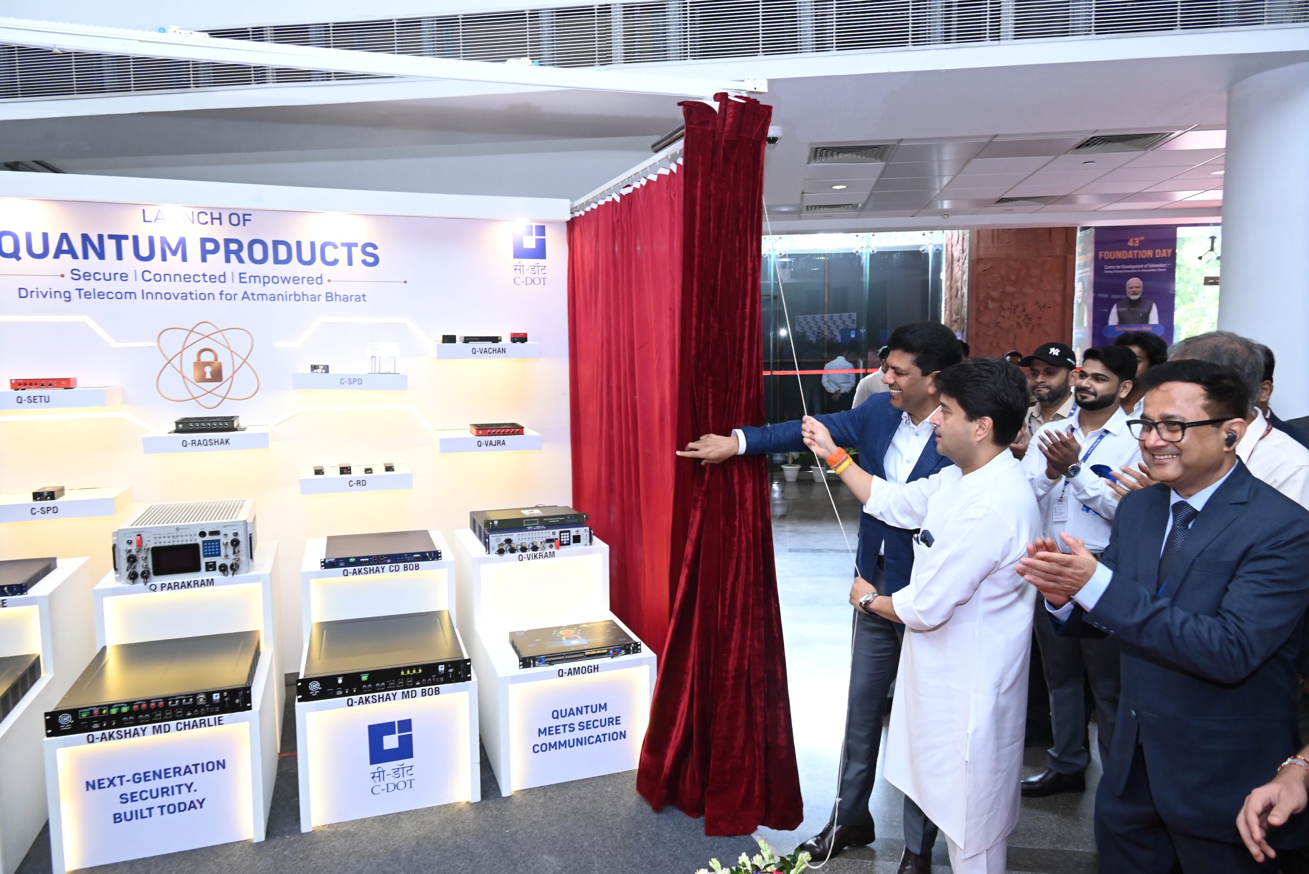
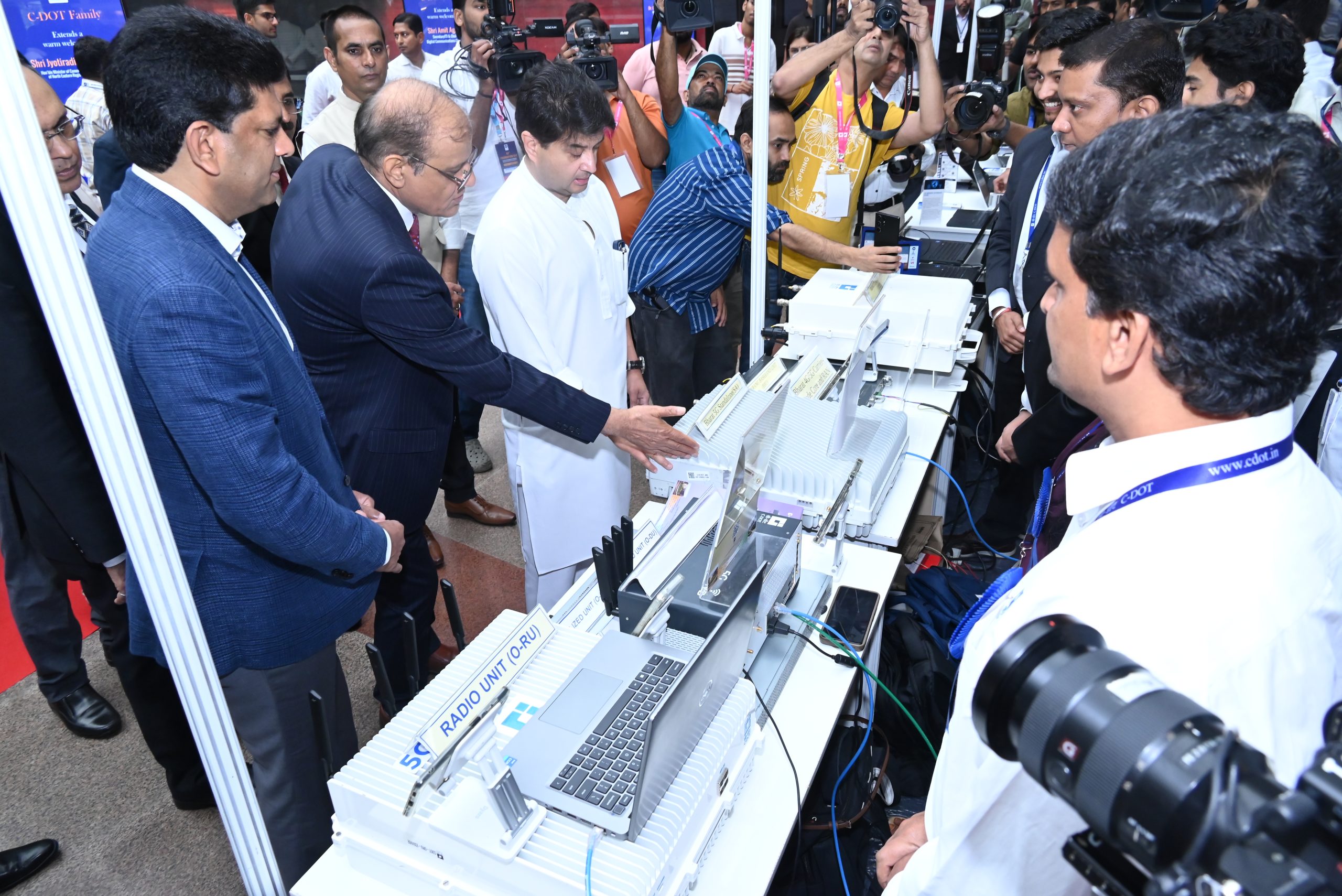
The Ministers also unveiled the Quantum Products Wall, showcasing C-DOT’s indigenous Quantum Series comprising of 14 products covering both Quantum Key Distribution (QKD) and Post-Quantum Cryptography (PQC) solutions developed to strengthen the security and resilience of India’s communication networks in the emerging quantum era. The product showcase at the exhibition, provided an opportunity to showcase C-DOT’s indigenous technologies and solutions across various domains of telecommunications. The dignitaries thereafter were briefed at the exhibition on the various indigenous telecom technologies and solutions developed by C-DOT.
During the inaugural session, the Hon’ble Ministers and senior dignitaries launched a Quantum Product booklet, which is a consolidation of C-DOT’s indigenous quantum solutions. The booklet presents C-DOT’s work in Quantum Key Distribution (QKD) and Post-Quantum Cryptography (PQC), highlighting the Centre’s efforts towards developing secure, resilient and future-ready communication technologies.
Addressing the gathering, Shri Jyotiraditya M. Scindia, Hon’ble Union Minister of Communications and Development of North Eastern Region, lauded C-DOT as an institution with the potential to transform not only India but also contribute to shaping the technological landscape globally. Highlighting C-DOT’s work in 5G, 6G, cybersecurity and disaster resilience, he emphasised the importance of taking indigenous innovations from the laboratory to the market. The Minister also highlighted the importance of strengthening indigenous research and innovation to create technologies that can serve national requirements and also position Indian technologies on the global stage.
He said that the spirit of “Atmanirbhar Bharat” and “Make in India” would attain its true potential when India not only develops technologies domestically but also “makes for the world”. Dedicating the occasion to C-DOT’s young engineers and researchers, he highlighted the true reflection of each letter of the name C-DOT in their Curiosity, spirit of Disruption, Ownership and Tenacity. He urged them to nurture their thirst for invention, challenge boundaries and harness their courage and capabilities to build technologies for the future, observing that the spirit of “Jai Vigyan, Jai Anusandhan” lies within the young minds of C-DOT.
Beyond Connectivity: Secure, Trusted and Intelligent Communication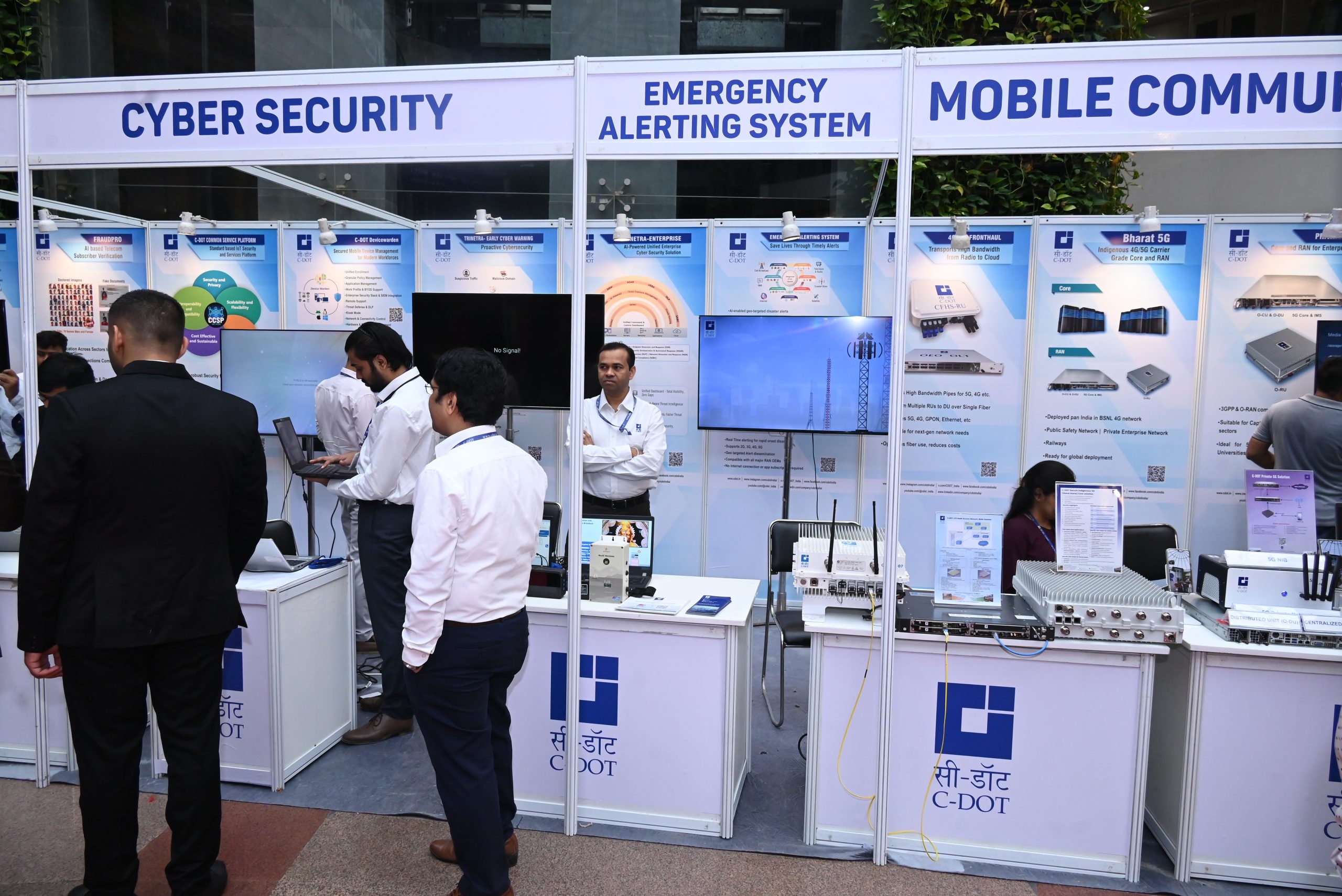
The Foundation Day celebrations focused around a day-long conference themed “Beyond Connectivity: Secure, Trusted and Intelligent Communication”. It brought together senior government officials, policy makers, industry leaders, technology experts and academia to deliberate on emerging technologies and the evolving communication landscape.
Speaking on the occasion, Dr. Rajkumar Upadhyay, CEO, C-DOT, said, “C-DOT’s journey over the past 42 years has been driven by its commitment to developing indigenous technologies for the nation. As telecommunications move beyond conventional connectivity, our focus is expanding towards secure, trusted and intelligent communication systems. Through our work in cybersecurity, quantum-secure communications, 6G and other emerging areas, C-DOT remains committed to strengthening India’s technological self-reliance and contributing to the development of globally competitive telecom technologies.”
The 43rd Foundation Day celebrations showcased C-DOT’s commitment to advancing indigenous research and innovation and contributing to the development of a secure, trusted and future-ready digital communications ecosystem. As it enters its 43rd year, C-DOT continues its research and development efforts in 6G, quantum-secure communications and other emerging technologies. This is in line with the vision of Atmanirbhar Bharat and India’s ambition of positioning the country as a global leader in next-generation, trusted connectivity.
Q-AKSHAY CD is a compact, fibre-based Quantum Key Distribution (QKD) system based on Coherent One Way (COW) and Differential Phase Shift (DPS) protocols in a compact 1U size. It enables secure quantum key generation and distribution over fibre networks.
Q-AKSHAY MD is a fibre-based QKD system based on the Measurement Device Independent (MDI) protocol, offering enhanced security against vulnerabilities associated with measurement devices. It represents C-DOT’s next-generation approach to secure quantum key distribution.
C-SPD is a Single-Photon Detector, a critical sub-module used in quantum communication systems.
C-RD is a wideband RF driver designed to drive intensity and phase modulators used in quantum communication systems. It serves as a critical sub-module for enabling high-performance quantum communication applications.
Q-SETU is a quantum-safe encryptor designed to secure Layer 3 communications with a throughput of up to 80 Mbps. It incorporates NIST Post-Quantum Cryptography (PQC) algorithms to protect data against emerging quantum-era threats.
Q-MAHASETU is a next-generation, commercial-grade quantum-safe encryptor supporting Layer 2/3 networks with throughput of up to 40 Gbps. It uses NIST PQC algorithms to provide high-speed, quantum-resistant protection for enterprise and critical communication networks.
Q-VIKRAM is a defence-grade quantum-safe encryptor providing up to 1 Gbps throughput for Layer 2/3 networks. It incorporates NIST PQC algorithms to provide enhanced protection for sensitive and strategic communications.
Q-AMOGH is a high-speed quantum-safe optical encryptor providing up to 200 Gbps throughput at Layer 1. Based on NIST PQC algorithms, it is designed to secure high-capacity optical communication links against emerging quantum threats.
Q-DARSHAN is a quantum-safe video IP phone incorporating NIST PQC algorithms to protect voice and video communications. It brings quantum-safe security directly into IP-based communication systems.
Q-VACHAN is quantum-safe In-line node for IP phone, NIST PQC algorithms, it can upgrade existing IP phones with quantum security.
Q-RAQSHAK is a quantum-safe enterprise network solution designed to protect enterprise communications and network infrastructure. It incorporates NIST PQC algorithms to provide protection against current and future cryptographic threats.
Q-VAAYU is a quantum-safe wireless point-to-point network solution designed to secure wireless communication links. It uses NIST PQC algorithms to provide quantum-resistant security for wireless connectivity.
Q-VAJRA1000 is a quantum-safe access node designed to upgrade existing communication networks with quantum security. It can support technologies such as GPON and wireless radios, enabling quantum-safe protection to be integrated into existing network infrastructure.
Q-PARAKRAM is a defence-grade quantum-safe encryptor providing up to 1 Gbps throughput for Layer 2/3 networks. It incorporates NIST PQC algorithms and is designed to provide robust quantum-resistant security for strategic and defence communications.
The post C-DOT, the Premier R&D Centre of DoT, Celebrates Its 43rd Foundation Day appeared first on ELE Times.
I recently designed 8 channel fully isolated RS-485 based Relay controller using CH42V003
 | submitted by /u/elcoanlanka [link] [comments] |
Saved my brother’s PS5 today
 | My brother (stupidly) had his PS5 on a floating shelf which gave way a couple of days ago. We found his PS5 dangling down by just the HDMI cord. Luckily, it mostly still worked but the HDMI port was damaged and the image was very poor and glitchy. I’ve been into electronics (mostly Arduino) for a couple of years now and even though I bought myself a hot air rework station a long time ago, it was my first time using it this weekend. We got a replacement HDMI kit from amazon and I did the replacement this evening. It took me quite a while to figure out the process but I’m glad to say he’s now gaming with a good image once again! [link] [comments] |
Важливі оновлення та новини корпоративного середовища Google Workspace for Education (домени @edu.kpi.ua та @lll.kpi.ua) для студентів і викладачів

Важливі оновлення та новини корпоративного середовища Google Workspace for Education (домени @edu.kpi.ua та @lll.kpi.ua) для студентів і викладачів
1️⃣ Масове перейменування поштових адрес студентських акаунтів (лише старші курси)
Sumitomo Chemical begins mass production of 4-inch InP epiwafers
Power from a candle: practical test of a thermoelectric module lamp
Latest issue of Semiconductor Today now available
Power Tips #156: How to design a high-boost-ratio boost converter

The maximum boost ratio achievable with a single stage, normally cited as 8-to-9, can be much higher if you keep important design considerations in mind.
In single-cell battery applications such as personal electronics or power tools, where the input voltage is less than 4V, you may need a high output voltage to reduce current in the system in order to provide higher power density, faster charging, improved efficiency and a small form factor. High-boost-factor designs allow a high ratio between the input and output voltage. This article discusses the process for designing a high-duty-cycle boost topology suitable for high-output-voltage applications, while showing the limits of achievable duty cycles and boost factors.
As a rule of thumb, the maximum boost ratio practically achievable with a single boost stage using regular silicon switches is often cited as 8-to-9. Much higher ratios are still possible, however, if you keep important design considerations in mind.
High-duty-cycle considerationsA boost converter can operate in either continuous conduction mode (CCM) or discontinuous conduction mode (DCM). In DCM, the inductor current reaches zero every switching cycle, whereas in CCM current always flows through the inductor. When operating in DCM, a combination of small inductance, low output current and low switching frequencies helps achieve a high boost ratio, as expressed by Equation 1.

Achieving a high boost ratio in CCM requires a high duty cycle, as shown by Equation 2.

While in theory a duty cycle of 99.9% (and a boost factor of 1,000) is possible, practical limitations exist. Most boost controller or converter integrated circuits have a maximum duty cycle dependent on switching frequency – typically in the range of 92% to 98%. Gate charge and other parasitics of the field-effect transistors (FETs) and printed circuit board traces limit the maximum duty cycle. Additionally, the higher the duty cycle, the lower the right-half-plane zero frequency becomes, which can result in a very slow regulation loop.
Choosing the switching frequencySelecting a switching frequency involves a trade-off between efficiency and solution size. For a high boost ratio, a lower switching frequency is preferable. When designing for DCM, the frequency must be low enough to maintain DCM operation for a given inductance value. Thus, a lower switching frequency directly helps achieve a higher boost factor in DCM.
In CCM, the switching frequency theoretically does not influence the maximum boost factor, but drive strength and metal-oxide semiconductor field-effect transistor (MOSFET) turnon and turnoff time will limit it in practice. If the driver is weak and the MOSFET switching speed is low, a lower switching frequency is better.
Choosing the inductorAs a rule of thumb, in CCM, an inductor current ripple between 15% and 40% of the maximum load current is preferable. A higher inductance value tends to increase peak efficiency, while a lower inductance value can achieve higher full-load efficiency.
For high boost ratios in CCM, the inductance may need to be high enough so that the internal slope compensation ramp is sufficient. As shown by Equation 3, the slope compensation ramp needs to be at least half of the sensed inductor current’s falling slope.

For a DCM design, the inductance needs to be small enough to operate in DCM at a full load for the given frequency. This can result in high peak currents. Operating in DCM is advantageous because it allows you to achieve a higher boost ratio. Typically, the inductor DC resistance (DCR) must remain small, since DCR has a strong effect on achievable performance.
Component-level design considerationsFor the MOSFET, the drain-to-source on-resistance (RDS(on)) must be small, since it has a strong influence on the achievable boost factor. Gate-drain (Qgd) and gate-source (Qgs) charges directly affect the rise and fall time of the switch, respectively, and become a limiting factor for achieving a high boost factor when the driver is weak or the switching frequency is too high.
The total gate charge (Qgate) compounds this issue further, demanding a stronger driver simply to keep switching losses and timing under control. The FET output capacitance, Coss, has a small impact on the maximum achievable boost factor, as long as it does not limit the duty cycle to a lower value than necessary.
This is precisely where gallium nitride (GaN) FETs offer a decisive advantage over silicon MOSFETs: their substantially lower Coss, Qgd, Qgs and Qgate enable much faster switching without requiring an oversized driver, removing this bottleneck and unlocking higher achievable boost ratios.
The output diode in synchronous designs does not significantly influence the boost factor, since its voltage drop occurs on the output side of the converter. A synchronous or nonsynchronous topology also has low impact in this regard.
Finally, both the output capacitor and input capacitor have low impact on the boost factor; for the input capacitor, this holds true as long as the input source is strong, meaning that it has low impedance.
High-boost-ratio design exampleFigure 1 shows a single-cell, 3V-to-42V boost converter using the LMG5126 integrated GaN boost converter from Texas Instruments (TI).

Figure 1 The TI 3V to 42V Synchronous GaN Boost Converter Reference Design uses the LMG5126 boost converter with integrated GaN FETs. Source: Texas Instruments
This design achieves an ultra-high-boost ratio of 14-to-1 while delivering up to 20W of output power and maintaining efficiency over 84%, as shown in Figure 2.

Figure 2 GaN FETs ensure over 84% efficiency at 600kHz. Source: Texas Instruments
To avoid the high peak currents associated with DCM operation, the converter operates in CCM, requiring a duty cycle of 93%. A 600kHz switching frequency minimizes the overall solution size. Figure 3 shows the resulting high-duty-cycle switch-node voltage.

Figure 3 This graph shows the LMG5126 boost converter’s switch-node voltage for VIN = 3V. Source: Texas Instruments
Inductor DCR and MOSFET RDS(on) have a high impact on achievable boost factor and should be priorities during component selection. FET rise and fall time may limit the maximum boost factor, and are closely tied to driver strength, gate resistor and FET parasitics. GaN FETs can help enable higher switching frequencies and will increase the boost factor.
Finally, it is essential to check the controller’s maximum duty cycle rating, since this may depend on switching frequency or other design parameters. Following these tips will help ensure success on your next high-boost-ratio converter design.

Florian Mueller is a systems engineer and Member Group Technical Staff in TI’s Power Supply Design Services group. He has a master’s degree in electrical engineering from the Technical University of Haag, Germany. Florian’s main focus lies on industrial high-voltage designs for different end equipment.

Moritz Mueller is an applications engineer at Texas Instruments. He has a master’s degree in electrical engineering from the University of Applied Sciences in Landshut, and mainly works on synchronous and nonsynchronous boost converter and flyback designs.
Related Content
- Power Tips #90: Get more boost from your boost converter
- Power Tips #115: How GaN switch integration enables low THD and high efficiency in PFC
- Power Tips #138: 3 ways to close the control loop for totem-pole bridgeless PFC
- Should you operate your step-down converter in power-save or forced PWM mode?
The post Power Tips #156: How to design a high-boost-ratio boost converter appeared first on EDN.
Pages



