
Feed aggregator
Apple CarPlay and Google Android Auto: Usage impressions and manufacturer tensions

What happens to manufacturers when your ability to differentiate whose vehicle you’re currently traveling in, far from piloting, disappears?
My wife’s 2018 Land Rover Discovery:

not only now has upgraded LED headlights courtesy of yours truly, I also persuaded the dealer a while ago to gratis-activate the vehicle’s previously latent Apple CarPlay and Google Android Audio facilities for us (gratis in conjunction with a fairly pricey maintenance bill, mind you…). I recently finally got around to trying them both out, and the concept’s pretty cool, with the implementation a close second. Here’s what CarPlay’s UI looks like, courtesy of Wikipedia’s topic entry:

And here’s the competitive Android Auto counterpart:

As you can see, this is more than just a simple mirroring of the default smartphone user interface; after the mobile device and vehicle successfully activate a bidirectional handshake, the phone switches into an alternative UI that’s more vehicle (specifically: mindful of driver-distraction potential) amenable, and tailored for its larger albeit potentially lower overall resolution dashboard-integrated display.
The baseline support for both protocols in our particular vehicle is wired, which means that you plug the phone into one of the USB-A ports located within the storage console located between the front seats. My wife’s legacy iPhone is still Lightning-based, so I’ve snagged both a set of inexpensive ($4.99 for three) coiled Lightning-to-USB-A cords for her:

and a similarly (albeit not quite as impressively) penny-pinching ($6.67 for two) suite of USB-C-to-USB-A coiled cords for my Google Pixel phones:

The wired approach is convenient because a single cord handles both communication-with-vehicle and phone charging tasks. That said, a lengthy strand of wire, even coiled, spanning the gap from the console to the magnetic mount located at the dashboard vent:

is aesthetically and otherwise unappealing, especially considering that the mount at the phone end also already redundantly supports both MagSafe (iPhone) and Qi (Pixel, in conjunction with a magnet-augmented case) charging functions:

Therefore, I’ve also pressed into service a couple of inexpensive (~$10 each, sourced from Amazon’s Warehouse-now-Resale section) wireless adapters that mimic the integrated wireless facilities of newer model-year vehicles and even comprehend both the CarPlay and Android Auto protocols. One comes from a retailer called VCARLINKPLAY:

The other is from the “PakWizz Store”:

The approach here is somewhat more complicated. The phone first pairs with the adapter, already plugged into and powered by the car’s USB-A port, over Bluetooth. The adapter then switches both itself and the phone to a common and (understandably, given the aggregate data payload now involved) beefier 5 GHz Wi-Fi Direct link.
Particularly considering the interference potential from other ISM band (both 2.4 GHz for Bluetooth and 5 GHz for Wi-Fi) occupants contending for the same scarce spectrum, I’m pleasantly surprised at how reliable everything is, although initial setup admittedly wasn’t tailored for the masses and even caused techie-me to twitch a bit.
Encroaching on vehicle manufacturers’ turfAs such, I’ve been especially curious to follow recent news trends regarding both CarPlay and Android Auto. Rivian and Tesla, for example, have long resisted adding support for either protocol to their vehicles, although rumors persist that both companies are continuing to develop support internally for potential rollout in the future.
Automotive manufacturers’ broader embrace (public at least) for next-generation CarPlay Ultra has to date been muted at best. And GM is actively phasing out both CarPlay and Android Auto from new vehicle models, in favor of an internally developed entertainment software-and-display stack alternative.
What’s going on? Consider this direct quote from Apple’s May 2025 CarPlay Ultra press release:
CarPlay Ultra builds on the capabilities of CarPlay and provides the ultimate in-car experience by deeply integrating with the vehicle to deliver the best of iPhone and the best of the car. It provides information for all of the driver’s screens, including real-time content and gauges in the instrument cluster.
Granted, Apple has noted that in developing CarPlay Ultra, it’s “reflecting the automaker’s look and feel” (along with “offering drivers a customizable experience”). But given that all Apple showed last May was an Aston Martin logo next to its own:
I’d argue that Apple’s “partnership” claims are dubious, and maybe even specious. And per comments from Ford’s CEO Jim Farley in a recent interview, he seems to agree (the full interview is excellent and well worth a read):
Are you going to allow OEMs to control the vehicles? How far do you want the Apple brand to go? Do you want the Apple brand to start the car? Do you want the Apple brand to limit the speed? Do you want the Apple brand to limit access?
The bottom line, as I see it, is that Apple can pontificate all it wants that:
CarPlay Ultra allows automakers to express their distinct design philosophy with the look and feel their customers expect. Custom themes are crafted in close collaboration between Apple and the automaker’s design team, resulting in experiences that feel tailor-made for each vehicle.
But automakers like Ford and GM are obviously (and understandably so, IMHO) worried that with Apple and Google already taking over key aspects of the visual, touch (and audible; don’t forget about the Siri and Google Assistant-now-Gemini voice) interfaces, not to mention their even more aggressive aspirations (along with historical behavior in other markets as a guide to future behavior here), the manufacturer, brand and model uniqueness currently experienced by vehicle occupants will evaporate in response.
More to comeI’ll be curious to see (and cover) how this situation continues to develop. For now, I welcome your thoughts in the comments on what I’ve shared so far in this post. And FYI, I’ve also got two single-protocol wireless adapter candidates sitting in my teardown pile awaiting attention: a CarPlay-only unit from the “Luckymore Store”:

And an Android Auto-only unit, the v1 AAWireless, which I’d bought several years back in its original Indiegogo crowdfunding form:

Stay tuned for those, as well!
—Brian Dipert is the Principal at Sierra Media and a former technical editor at EDN Magazine, where he still regularly contributes as a freelancer.
Related Content
The post Apple CarPlay and Google Android Auto: Usage impressions and manufacturer tensions appeared first on EDN.
Is this low-inductance power-device package the real deal?

While semiconductor die get so much of the attention due to their ever-shrinking feature size and ever-increasing substrate size, the ability to effectively package them and thus use them in a circuit is also critical. For this reason, considerable effort is devoted to developing and perfecting practical, technically advanced, thermally suitable cost-effective packages for components ranging from switching power devices to multi-gigahertz RF devices.
Regardless of frequency, package parasitic inductance is a detrimental issue, as it slows down slewing needed for switching crispness of digital devices and responsiveness of analog ones (of course, reality is that digital switching performance is still constrained by analog principles.).
Now, a researcher team at the US Department of Energy’s National Renewable Energy Laboratory (NREL; recently renamed as the National Laboratory of the Rockies) has developed a silicon-carbide half-bridge module that uses organic direct-bonded copper in a novel layout design to enable a high degree of magnetic-flux cancellation, Figure 1.
 Figure 1 (left) 3D CAD drawing of new half-bridge inverter module; (right) Early prototype of polyimide-based half-bridge module. Source: NREL
Their Ultra-Low Inductance Smart (ULIS) package is a 1200 V, 400 A half bridge silicon carbide (SiC) power module that can be pushed beyond 200-kHz switching frequency at maximum power. The low-cost ULIS also allows the converter to become easier to manufacture, addressing issues related to both bulkiness and costs.
Preliminary results show that it has approximately seven to nine times lower loop inductances and higher switching speeds at similar voltages/current levels, and five times the energy density of earlier designs — while occupying a smaller footprint, Figure 2.

Figure 2 The complete ULIS package is very different than conventional packages and offers far lower loop inductance compared to exiting approaches. Source: NREL
In addition to being powerful and lightweight, the module continuously tracks its own condition and can anticipate component failures before they happen.
In traditional designs, the power modules conduct electricity and dissipate excess heat by bonding copper sheets directly to a ceramic base—an effective, but rigid, solution. ULIS bonds copper to a flexible Dupont Temprion polymer create a thinner, lighter, more configurable design.
Unlike typical power modules which assemble semiconductor devices inside a brick-like package, ULIS winds its circuits around a flat, octagonal design, Figure 3. The disk-like shape allows more devices to be housed in a smaller area, making the overall package smaller and lighter.

Figure 3 This “exploded” drawing of the complete half-bridge power module shows the arrangement of the electrical and structural elements. Source: NREL
At the same time, its novel current routing allows for maximum cancellation of magnetic flux, contributing to the power module’s clean, low-loss electrical output, meaning ultrahigh efficiency.
While conventional power modules rely on bulky and inflexible materials, ULIS takes a new approach. Traditional designs call for power modules to conduct electricity and dissipate excess heat by bonding copper sheets directly to a ceramic base—an effective but rigid solution. ULIS bonds copper to the flexible, electrically insulating Temprion to create a thinner and lighter module.
The stacked module layout greatly improves energy density and reduces parasitic inductance (based on simulation data). Typical half-bridge module inductance is 2.2 to 5.5 nanohenries, compared to 20 to 25 nH for existing designs. Further, reliability is enhanced as the compliance of Temprion reduces the strain caused by the differences in the coefficient of thermal expansion (CTE) between mated materials.
Since the material bonds easily to copper using just pressure and heat, and because its parts can be machined using widely available equipment, the team maintains that the ULIS can be fabricated quickly and inexpensively, with manifesting costs in the hundreds of dollars rather than thousands, Figure 4.

Figure 4 The ULIS can be machined using widely available equipment, thus significantly reducing the manufacturing costs for the power module. Source: NREL
Another innovation allows the ULIS to function wirelessly as an isolated unit that can be controlled and monitored without external cables. A patent is pending for this low-latency wireless communication protocol.
The ULIS design is a good example of the challenges and dead-end paths that innovation can take on its path to a successful conclusion. According to the team’s report, one of the original layouts looked like a flower with a semiconductor at the tip of each petal. Another idea was to create a hollow cylinder with components wired to the inside.
Every idea the team came up with was either too expensive or too difficult to fabricate—until they stopped thinking in three dimensions and flattened the design into nearly two dimensions, which made it possible to build the module balancing complexity with cost and performance.
The details of the work are in their readable and detailed IEEE APEC paper “Organic Direct Bonded Copper-Based Rapid Prototyping for Silicon Carbide Power Module Packaging” but it is behind a paywall. However, there is a nice “poster” summary of their work posted at the NLR site here.
I wonder is this innovation will catch on and be adopted, but I certainly don’t know. What I do know is that some innovations are slow to catch on, and many do not because of real-world problems related to scaling up, volume production unforeseen technical issues, testability…it’s a long list of what can get in the way.
If you don’t think so, just look at batteries: every month, we see news of dramatic advances that will supposedly revolutionize their performance, yet these breakthroughs don’t seem to get traction. Sometimes it is due to technical or implementation problems, but often it is because the actual improvement they provide does not outweigh the disruption they create in getting there.
Bill Schweber is an EE who has written three textbooks, hundreds of technical articles, opinion columns, and product features.
Related content
- Stop blaming the supply for your dissipation woes
- GaN gets game
- New Horizons spacecraft’s power issues make yours look trivial
- Paralleling supplies: good, bad, or ugly?
The post Is this low-inductance power-device package the real deal? appeared first on EDN.
Top 10 edge AI chips

As edge devices become increasingly AI-enabled, more and more chips are emerging to fill every application niche. At the extremes, applications such as speech recognition can be done in always-on power envelopes, while tens of watts will be enough for even larger generative AI models today.
Here, in no particular order, are 10 of EDN’s selections for a range of edge AI applications. These devices range from those capable of handling multimodal large language models (LLMs) in edge devices to those designed for vision processing and minimizing power consumption for always-on applications.
Multiple camera streamsFor vision applications, Ambarella Inc.’s latest release is the CV7 edge AI vision system-on-chip (SoC) for processing multiple high-quality camera streams simultaneously via convolutional neural networks (CNNs) or transformer networks. The CV7 features the latest generation of Ambarella’s proprietary AI accelerator, plus an in-house image-signal processor (ISP), which uses both traditional ISP algorithms and AI-driven features. This family also includes quad Arm Cortex-A73 cores, hardware video codecs on-chip, and a new, 64-bit DRAM interface.
Ambarella is targeting this family for AI-based 8K consumer products such as action cameras, multicamera security systems, robotics and drones, industrial automation, and video conferencing. It will also be suitable for automotive applications such as telematics and advanced driver-assistance systems.
 Ambarella’s CV7 vision SoC (Source: Ambarella Inc.)
Fallback CPU
Ambarella’s CV7 vision SoC (Source: Ambarella Inc.)
Fallback CPU
The MLSoC Modalix from SiMa Technologies Inc. is now available in production quantities, along with its LLiMa software framework for deployment of LLMs and generative AI models on Modalix. Modalix is SiMa’s second-generation architecture, which comes as a family of SoCs designed to host full applications.
Modalix chips have eight Arm A-class CPU cores on-chip alongside the accelerator, important for running application-level code, but also allows programs to fall back on the CPU just in case a particular math operation isn’t supported by the accelerator. Also on the SoC are an on-chip ISP and digital-signal processor (DSP). Modalix will come in 25-, 50-, 100-, and 200-TOPS (INT8) versions. The 50-TOPS version will be first to market and can run Llama2-7B at more than 10 tokens per second, with a power envelope of 8–10 W.
Open-source NPUSynaptics Inc.’s Astra series of AI-enabled IoT SoCs range from application processors to microcontroller (MCU)-level parts. This family is purpose-built for the IoT.
The SL2610 family of multimodal edge AI processors is for applications between smart appliances, retail point-of-sale terminals, and drones. All parts in the family have two Arm Cortex-A55 cores, and some have a neural processing unit (NPU) subsystem. The Coral NPU included was developed at Google—it’s an open-source RISC-V CPU with scalar instructions—sitting alongside Synaptics’ homegrown AI accelerator, the T1, which offers 1-TOPS (INT8) performance for transformers and CNNs.
 Synaptics’ SL2610 multimodal edge AI processors (Source: Synaptics Inc.)
Raspberry Pi compatibility
Synaptics’ SL2610 multimodal edge AI processors (Source: Synaptics Inc.)
Raspberry Pi compatibility
The Hailo-10H edge AI accelerator from Hailo Technologies Ltd. is gaining a large developer base, as it is available in a form factor that plugs into hobbyist platform Raspberry Pi. However, the Hailo-10H is also used by HP in add-on cards for its point-of-sale systems, and it’s also automotive-qualified.
The 10H is the same silicon as the Hailo-10 but runs at a lower power-performance point: The 10H can run 2B-parameter LLMs in about 2.5 W. The architecture of this AI co-processor is based on Hailo’s second-generation architecture, which has improved support for transformer architectures and more flexible number representation. Multiple models can be inferenced concurrently.
 Hailo’s Hailo-10H edge AI accelerator (Source: Hailo Technologies Ltd.)
Analog acceleration
Hailo’s Hailo-10H edge AI accelerator (Source: Hailo Technologies Ltd.)
Analog acceleration
Startup EnCharge AI announced its first product, the EN100. This chip is a 200-TOPS (INT8) accelerator targeted squarely at the AI PC, achieving an impressive 40 TOPS/W. The device is based on EnCharge’s capacitance-based analog compute-in-memory technology, which the company says is less temperature-sensitive than resistance-based schemes. The accelerator’s output is a voltage (not a current), meaning transimpedance amplifiers aren’t needed, saving power.
Alongside the analog accelerator on-chip are some digital cores that can be used if higher precision is required, or floating-point maths. The EN100 will be available on a single-chip M.2 card with 32-GB LPDDR, with a power envelope of 8.25 W. A four-chip, half-height, half-length PCIe card offers up to 1 TOPS (INT8) in a 40-W power envelope, with 128-GB LPDDR memory.
 Encharge AI’s EN100 M.2 card (Source: Encharge AI)
SNNs
Encharge AI’s EN100 M.2 card (Source: Encharge AI)
SNNs
For microwatt applications, Innatera Nanosystems B.V. has developed an AI-equipped MCU that can run inference at very, very low power. The Pulsar neuromorphic MCU targets always-on sensor applications: It consumes 600 µW for radar-based presence detection and 400 µW for audio scene classification, for example.
The neural processor uses Innatera’s spiking neural network (SNN) accelerators—there are both analog and digital spiking accelerators on-chip, which can be used for different types of applications and workloads. Innatera says its software stack, Talamo, means developers don’t have to be SNN experts to use the device. Talamo interfaces directly with PyTorch and a PyTorch-based simulator and can enable power consumption estimations at any stage of development.
 Innatera’s Pulsar spiking neural processor (Source: Innatera Nanosystems B.V.)
Generative AI
Innatera’s Pulsar spiking neural processor (Source: Innatera Nanosystems B.V.)
Generative AI
Axelera AI’s second-generation chip, Europa, can support both multi-user generative AI and computer vision applications in endpoint devices or edge servers. This eight-core chip can deliver 629 TOPS (INT8). The accelerator has large vector engines for AI computation alongside two clusters of eight RISC-V CPU cores for pre- and post-processing of data. There is also an H.264/H.265 decoder on-chip, meaning the host CPU can be kept free for application-level software. Given the importance of ensuring compute cores are fed quickly with data from memory, the Europa AI processor unit provides 128 MB of L2 SRAM and a 256-bit LPDDR5 interface.
Axelera’s Voyager software development kit covers both Europa and the company’s first-generation chip, Metis, reserved for more classical CNNs and vision tasks. Europa is available both as a chip or on a PCIe card. The cards are intended for edge server applications in which processing multiple 4K video streams is needed.
Butter wouldn’t meltMost members of the DX-M1 series from South Korean chip company DeepX Co. Ltd. provide 25-TOPS (INT8) performance in the 2- to 5-W power envelope (the exception being the DX-M1M-L, offering 13 TOPS). One of the company’s most memorable demos involves placing a blob of butter directly on its chip while running inference to show that it doesn’t get hot enough for the butter to melt.
Delivering 25 TOPS in this co-processor chip is plenty for vision tasks such as pose estimation or facial recognition in drones, robots, or other camera systems. Under development, the DX-M2 will run generative AI workloads at the edge. Part of the company’s secret sauce is in its quantization scheme, which can run INT8-quantized networks with accuracy comparable to the FP32 original. DeepX sells chips, modules/cards, and small, multichip systems based on its technology for different edge applications.
Voice interfaceThe latest ultra-low-power edge AI accelerator from Syntiant Corp., the NDP250, offers 5× the tensor throughput versus its processor. This device is designed for computer vision, speech recognition, and sensor data processing. It can run on as little as microwatts, but for full, always-on vision processing, the consumption is closer to tens of milliwatts.
As with other parts in Syntiant’s range, the devices use the company’s AI accelerator core (30 GOPS [INT8]) alongside an Arm Cortex-M0 MCU core and an on-chip Tensilica HiFi 3 DSP. On-chip memory can store up to 6-million-bit parameters. The NDP250’s DSP supports floating-point maths for the first time in the Syntiant range. The company suggests that the ability to run both automatic speech recognition and text-to-speech models will lend the NDP250 to voice interfaces in particular.
Multiple power modesNvidia Corp.’s Jetson Orin Nano is designed for AI in all kinds of edge devices, targeting robotics in particular. It’s an Ampere-generation GPU module with either 8 GB or 4 GB of LPDDR5. The 8-GB version can do 33 TOPS (dense INT8) or 17 TFLOPS (FP16). It has three power modes: 7-W, 15-W, and a new, 25-W mode, which boosts memory bandwidth to 102 GB/s (from 65 GB/s for the 15-W mode) by increasing GPU, memory, and CPU clocks. The module’s CPU has six Arm Cortex-A78AE 64-bit cores. Jetson Orin Nano will be a good fit for multimodal and generative AI at the edge, including vision transformer and various small language models (in general, those with <7 billion parameters).
 Nvidia’s Jetson Orin Nano (Source: Nvidia Corporation)
The post Top 10 edge AI chips appeared first on EDN.
Spectral Engineering and Control Architectures Powering Human-Centric LED Lighting
As technological advancements continue to pursue personalisation & customisation at every level, illumination has also transformed from a need to a customisation. Consequently, the LED industry is moving towards a similar yet prominent stride, making customised and occasion-specific solutions, keeping in consideration the human behaviour and lighting changes across the day. Long seen as the constant and uniform thing, illumination is now being reimagined as something dynamic and customisable.
In the same pursuit, the industry has moved towards enabling Human-Centric Lighting(HCL), where lighting is designed and engineered to emulate natural daylight, ranging from dimming them as the Sun goes down, while brightening up as the day begins. Gradually, illumination is now being designed around human biology, visual comfort, and cognitive performance rather than simple brightness or energy efficiency.
But what lies behind this marvel is hardcore engineering. Technically, the result is made possible by the marvels of spectral engineering & control architectures, wherein the former adjusts the light spectrum while the latter enables the intelligence directing the timing changes of the lighting system. Simultaneously, the dual play brings forth today’s human-centric lighting into real-life examples and is also making them more customised and personalised. This ultimately helps in supporting human circadian rhythms, enhancing well-being, mood, and performance.
To enable these engineered outcomes, embedded sensors, digital drivers, and networked control platforms are integrated into the modern-day LED lights, transforming illumination into a responsive, data-driven infrastructure layer. In combination, spectral engineering and intelligent control systems are reshaping the capabilities of LED lighting, transforming it from a passive utility into a dynamic, precision-engineered tool for enhancing human wellbeing, productivity, and performance.
How is Spectral Power Distribution engineered?
When we talk about LED lights, white light is the first thing that comes to our minds. Although the same is not true scientifically. Surprisingly, LEDs inherently emit blue light and not white. To turn the blue light into white, a Phosphor coating is applied over it. Consequently, the blue light mixes with the phosphor to turn some of the light into green, red & yellow simultaneously. These lights eventually mix to turn white.
Spectral Power Distribution (SPD) is simply the profile of the white colour which is not visible to our naked eyes, and how much of each colour is present in the visible white light. The final light can be controlled by various means, such as the type of phosphor, how thick the phosphor layer is, or by adding extra coloured LEDs (like red or cyan).
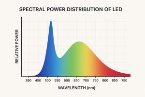
Spectral Power Distribution is engineered by carefully mixing different colours of light inside an LED, even though it looks white, so that the light feels right for the human body and mind.
Engineering the Spectral Power Distribution of White LEDs
Often, it is seen that the very same white light is sometimes harsh while sometimes soft- all this is because of various variables. Today, from being a static character, SPD has turned into a tunable design parameter,++ becoming a Controllable Design Variable. To this effect, SPD is largely controlled by Phosphor composition (which colours it emits), Particle size and density, and finally Layer thickness and distribution.
That’s why the same 400K LEDs from different manufacturers can feel completely different — their SPDs are different, even if the Correlated Color Temperature (CCT) is the same. But as long as the final color is decided by some application made during manufacturing, the effect remains static. While spectral Power distribution is essential, it is equally important to dictate the given behaviour as per the time of the day.
Multi-Channel LED Configurations for Spectral Tunability
To enable a real-time nature to this Spectral tunability, engineers today use multiple LED channels, including:
- White + Red
- White + Cyan
- RGBW / RGBA
- Tunable white (warm white + cool white)
By precisely varying the current supplied to each LED channel, the spectral power distribution can be reshaped in real time, allowing the system to shift between blue-enriched and blue-reduced lighting modes as required. This level of control allows you to adjust the perceived colour temperature independently of the light’s biological impact, rather than having them locked together. As a result, SPD is no longer a fixed characteristic of the light source but becomes a dynamic, real-time controllable design parameter.
Melanopic Response, Circadian Metrics, and Spectral Weighting
When we talk about light, visibility & brightness make up the primary issue, but that has changed drastically with the emergence of Human Centric Lighting (HCL). With HCL coming into play, photopic lux, the quantification of brightness, is no longer a go-to metric to decide upon the quality of lighting. It is because it explained only one part of the coin, which is visibility, and not how this light or visibility affects human biology.
At the same time, Human Centered Lighting focuses on how light affects the circadian system, alertness, sleep–wake cycles, mood, and hormonal regulation. This phenomenon has brought up new metrics that tell us not only about the brightness or visibility, but also how it biologically acts. One such metric is Melanopic Lux, which weights the spectrum based on melanopsin sensitivity. Melanopsin is a photopigment in our eyes, usually sensitive to Blue-Cyan light.
Interestingly, more melanopic stimulation → increased alertness and circadian activation, while less melanopic stimulation → relaxation and readiness for sleep. That’s where we come to the core of our subject – Light induced behaviuour. The emergence of Melanopic Lux allows engineers to decouple visual brightness from biological effect, giving the right direction to Human Centric Lighting.
While melanopic metrics define what kind of biological response light should produce, control architectures determine when and how that response is delivered. Translating circadian intent into real-world lighting behaviour requires intelligent control systems capable of dynamically adjusting spectrum, intensity, and timing throughout the day. This is where embedded sensors, digital LED drivers, and networked control platforms come into play, enabling lighting systems to modulate melanopic content in real time—boosting circadian stimulation during the day and reducing it in the evening—without compromising visual comfort or energy efficiency.
Other metrics, such as Melanopic Equivalent Daylight Illuminance (EDI) and Circadian Stimulus (CS) are used to quantify how effectively a light source supports circadian activation or melatonin suppression, beyond what photopic lux can describe.
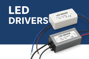
LED Drivers and Power Electronics for Dynamic Spectral Control
In human-centric lighting systems, LED drivers are no longer simple power supplies but precision control elements that translate circadian intent into real-world illumination. Because LEDs are current-driven devices, accurate current regulation is essential to maintain stable brightness and spectral output, especially as temperature and operating conditions change.
Dynamic spectral tuning typically relies on multi-channel LED architectures, making channel balancing a critical requirement. Each LED colour behaves differently electrically and thermally, and without independent, well-balanced current control, the intended spectral profile can drift over time, affecting both visual quality and biological impact.
Equally important is dimming accuracy. Human-centric lighting demands smooth, flicker-free dimming that preserves spectral integrity at all brightness levels, particularly during low-light, evening scenarios. Advanced driver designs enable fine-grained dimming and seamless transitions, allowing lighting systems to dynamically adjust spectrum and intensity throughout the day while maintaining visual comfort and circadian alignment.
System Integration Challenges and Design Trade-Offs
While human-centric lighting promises precise control over both visual and biological responses, delivering this in real-world systems involves significant integration challenges and design trade-offs. Spectral accuracy, electrical efficiency, thermal management, and system cost must all be balanced within tight form-factor and reliability constraints. Multi-channel LED engines increase optical and control complexity, while higher channel counts demand more sophisticated drivers, sensing, and calibration strategies.
Thermal effects further complicate integration, as LED junction temperature directly influences efficiency, colour stability, and lifetime. Without careful thermal design and feedback control, even well-engineered spectral profiles can drift over time. At the same time, adding sensors, networking, and intelligence introduces latency, interoperability, and cybersecurity considerations that must be addressed at the system level.
Ultimately, successful human-centric lighting solutions are defined not by any single component, but by holistic co-design—where optics, power electronics, controls, and circadian metrics are engineered together. The trade-offs made at each layer determine whether a system merely adjusts colour temperature or truly delivers biologically meaningful, reliable, and scalable lighting performance.
The post Spectral Engineering and Control Architectures Powering Human-Centric LED Lighting appeared first on ELE Times.
Dell Technologies Enables NxtGen to Build India’s Largest AI Factory
Story Highlights
Dell AI Factory with NVIDIA to provide scalable and secure infrastructure for NxtGen’s AI platform, India’s first and largest AI factory, enabling national-scale AI development.
This milestone deployment accelerates India’s AI mission, enabling large‑scale generative, agentic, and physical AI while expanding NxtGen’s high‑performance AI services nationwide.
Dell Technologies today announced that NxtGen AI Pvt Ltd, one of India’s foremost sovereign cloud and AI infrastructure providers, has selected Dell AI Factory with NVIDIA solutions for building India’s first and largest dedicated AI factory. This milestone deployment will significantly expand India’s national AI capability, enabling large-scale generative AI, agentic AI, physical AI, and high-performance computing across enterprises, start-ups, and government programs.
Dell will provide the core infrastructure, including Vertiv liquid-cooled Dell PowerEdge XE9685L servers, delivered through Dell Integrated Rack Scalable Systems, for NxtGen’s new AI cluster, empowering the company to meet the growing demand for AI as a Service and large-scale GPU capacity.
Why it matters
This accelerated computing infrastructure is vital for advancing India’s AI mission, significantly expanding NxtGen’s AI cloud services for a diverse range of clients, from start-ups to academia and government. By empowering NxtGen with this advanced foundation, Dell is accelerating India’s next wave of AI development and innovation, ensuring critical access to high-performance AI capabilities across the region.
Powering the future of AI with advanced Dell AI infrastructure
The Dell AI Factory with NVIDIA combines AI infrastructure, software, and services in an advanced, full-stack platform designed to meet the most demanding AI workloads and deliver scalable, reliable performance for training and inference. Leveraging the Dell AI Factory with NVIDIA, NxtGen will deploy Vertiv liquid-cooled, fully integrated Dell IR5000 racks featuring Dell PowerEdge XE9685L servers with the NVIDIA accelerated computing platform to build a cluster with over 4,000 NVIDIA Blackwell GPUs, NVIDIA BlueField-3 DPUs, and NVIDIA Spectrum-X Ethernet networking, all purpose-built for AI. These will be complemented by Dell PowerEdge R670 servers and Dell PowerScale F710 storage.
Dell AI Factory with NVIDIA: Empowering AI for Human Progress
The Dell AI Factory with NVIDIA offers a full stack of AI solutions from data center to edge, enabling organizations to rapidly adopt and scale AI deployments. The integration of Dell’s AI capabilities with NVIDIA’s accelerated computing, networking, and software technologies provides customers with an extensive AI portfolio and an open ecosystem of technology partners. With more than 3,000 customers globally, the Dell AI Factory with NVIDIA reflects Dell’s leadership in enabling enterprises with scalable, secure and high-performance AI infrastructure.
The comprehensive Dell AI Factory with NVIDIA portfolio provides a simplified and reliable foundation for NxtGen to deliver advanced AI capabilities at speed and scale. This allows NxtGen to deliver on its core mission of providing sovereign, cost-effective and powerful AI services that help businesses grow and innovate, while at the same time reinforcing Dell’s commitment to providing the technology that drives human progress.
By equipping organizations like NxtGen with cutting-edge AI infrastructure and services, Dell is helping to unlock new possibilities and create a future where technology empowers everyone to achieve more.
Perspectives
“India’s rapid AI growth demands strong, reliable, and future-ready infrastructure,” said Manish Gupta, president and managing director, India, Dell Technologies. “Dell Technologies is addressing this need through the Dell AI Factory with NVIDIA, designed to simplify and scale AI deployments across industries. As the top AI infrastructure provider, we are enabling this shift by combining storage, compute, networking and software to accelerate AI adoption. Our collaboration with NxtGen brings these capabilities closer to Indian enterprises, helping them deploy AI efficiently and cost-effectively. This marks another step in our commitment to empowering India’s digital future through secure, scalable, and sovereign AI infrastructure.”
“NxtGen is committed to building India’s AI backbone,” said A. S. Rajgopal, managing director and chief executive officer, NxtGen. “This deployment marks a significant milestone for the country: India’s largest AI model-training cluster, built and operated entirely within India’s sovereign cloud framework. Dell Technologies has been critical in enabling this scale, performance, and reliability. Together, we are unlocking the infrastructure that will power the next generation of Indian AI models and applications.”
“India’s ambitious AI mission requires a foundation of secure, high-performance accelerated computing infrastructure to enable model and AI application development,” said Vishal Dhupar, managing director, Asia South, NVIDIA. “Dell’s integration of NVIDIA AI software and infrastructure, including NVIDIA Blackwell GPUs and NVIDIA Spectrum-X networking, provides the AI factory resources to help NxtGen accelerate this critical national capability.”
The post Dell Technologies Enables NxtGen to Build India’s Largest AI Factory appeared first on ELE Times.
Quest Global Appoints Richard Bergman as Global Business Head of its Semiconductor Division
Bengaluru, India, January 28th, 2026 – Quest Global, the world’s largest independent pure-play engineering services company, today announced the appointment of Richard (Rick) Bergman as President & Global Business Head of its Semiconductor vertical.
As the Global Business Head, Rick will focus on shaping the division’s long-term strategy, accelerating revenue growth, and deepening relationships with global customers. His responsibilities include defining a multi-year growth roadmap, supporting clients’ success through high-impact and transformational solutions, especially in AI, automotive, and industrial sectors, and fostering a culture of innovation and operational excellence to meet next-generation engineering demands.
“The semiconductor industry is at a turning point, fueled by AI, system innovation, and shifting supply chains,” says Ajit Prabhu, Co-Founder and CEO, Quest Global. “Rick is a fantastic addition to our team. He brings incredible leadership across semiconductors and computing, plus a real talent for scaling organizations and building genuine, long-term relationships with customers. Bringing him on board is a clear sign of our commitment to growing this vertical and making sure Quest Global remains a humble, trusted partner for engineering and transformation in this space.”
“Semiconductors are the foundational enablers of innovation across AI, high-performance computing, automotive, communications, and industrial systems,” said Rick Bergman, President & Global Business Head – Semiconductor, Quest Global. “What attracted me to Quest Global is the company’s unique combination of deep engineering DNA, global scale, and a long-term partnership mindset with customers. As the industry navigates increasing complexity, my focus will be on helping customers solve their most critical engineering challenges while building a scalable, high-impact business.”
Rick brings more than two decades of leadership experience across semiconductors, computing, graphics, and advanced technology platforms. Most recently, he served as President and CEO of Kymeta Corporation. Previously, he held senior leadership roles at AMD, Synaptics, and ATI Technologies. Throughout his career, Rick has led multi-billion-dollar businesses, overseen major acquisitions, and built high-performing global teams.
This appointment underscores Quest Global’s commitment to building category-leading leadership and scaling its Semiconductor business, aligned with evolving customer needs.
About Quest Global
At Quest Global, it’s not just what we do but how and why we do it that makes us different. We’re in the business of engineering, but what we’re really creating is a brighter future. For over 25 years, we’ve been solving the world’s most complex engineering problems. Operating in over 18 countries, with over 93 global delivery centers, our 21,500+ curious minds embrace the power of doing things differently to make the impossible possible. Using a multi-dimensional approach, combining technology, industry expertise, and diverse talents, we tackle critical challenges faster and more effectively. And we do it across the Aerospace & Defense, Automotive, Energy, Hi-Tech, MedTech & Healthcare, Rail and Semiconductor industries. For world-class end-to-end engineering solutions, we are your trusted partner.
The post Quest Global Appoints Richard Bergman as Global Business Head of its Semiconductor Division appeared first on ELE Times.
VIS licenses TSMC’s 650V and 80V GaN technology
Round pegs, square holes: Why GPGPUs are an architectural mismatch for modern LLMs

The saying “round pegs do not fit square holes” persists because it captures a deep engineering reality: inefficiency most often arises not from flawed components, but from misalignment between a system’s assumptions and the problem it is asked to solve. A square hole is not poorly made; it’s simply optimized for square pegs.
Modern large language models (LLMs) now find themselves in exactly this situation. Although they are overwhelmingly executed on general-purpose graphics processing units (GPGPUs), these processors were never shaped around the needs of enormous inference-based matrix multiplications.
GPUs dominate not because they are a perfect match, but because they were already available, massively parallel, and economically scalable when deep learning began to grow, especially for training AI models.
What follows is not an indictment of GPUs, but a careful explanation of why they are extraordinarily effective when the workload is rather dynamic and unpredictable, such as graphic processing, and disappointedly inefficient when the workload is essentially regular and predictable, such as AI/LLM inference execution.
The inefficiencies that emerge are not accidental; they are structural, predictable, and increasingly expensive as models continue to evolve.
Execution geometry and the meaning of “square”
When a GPU renders a graphic scene, it deals with a workload that is considerably irregular at the macro level, but rather regular at the micro level. A graphic scene changes in real time with significant variations in content—changes in triangles and illumination—but in an image, there is usually a lot of local regularity.
One frame displays a simple brick wall, the next, an explosion creating thousands of tiny triangles and complex lighting changes. To handle this, the GPU architecture relies on a single-instruction multiple threads (SIMT) or wave/warp-based approach where all threads in a “wave” or “warp,” usually between 16 and 128, receive the same instruction at once.
This works rather efficiently for graphics because, while the whole scene is a mess, local patches of pixels are usually doing the same thing. This allows the GPU to be a “micro-manager,” constantly and dynamically scheduling these tiny waves to react to the scene’s chaos.
However, when applied to AI and LLMs, the workload changes entirely. AI processing is built on tensor math and matrix multiplication, which is fundamentally regular and predictable. Unlike a highly dynamic game scene, matrix math is just an immense but steady flow of numbers. Because AI is so consistent, the GPU’s fancy, high-speed micro-management becomes unnecessary. In this context, that hardware is just “overhead,” consuming power and space for a flexibility that the AI doesn’t actually use.
This leaves the GPGPU in a bit of a paradox: it’s simultaneously too dynamic and not dynamic enough. It’s too dynamic because it wastes energy on micro-level programming and complex scheduling that a steady AI workload doesn’t require. Yet it’s not dynamic enough because it is bound by the rigid size of its “waves.”
If the AI math doesn’t perfectly fit into a warp of 32, the GPU must use “padding,” effectively leaving seats empty on the bus. While the GPU is a perfect match for solving irregular graphics problems, it’s an imperfect fit for the sheer, repetitive scale of modern tensor processing.
Wasted area as a physical quantity
This inefficiency can be understood geometrically. A circle inscribed in a square leaves about 21% of the square’s area unused. In processing hardware terms, the “area” corresponds to execution lanes, cycles, bandwidth, and joules. Any portion of these resources that performs work that does not advance the model’s output is wasted area.
The utilization gap (MFU)
The primary way to quantify this inefficiency is through Model FLOPs Utilization (MFU). This metric measures how much of the chip’s theoretical peak math power is actually being used for the model’s calculations versus how much is wasted on overhead, data movement, or idling.
For an LLM like GPT-4 running on GPGPT-based accelerators operating in interactive mode, the MFU drops by an order of magnitude with the hardware busy with “bookkeeping,” which encompasses moving data between memory levels, managing thread synchronization, or waiting for the next “wave” of instructions to be decoded.
The energy cost of flexibility
The inefficiency is even more visible in power consumption. A significant portion of that energy is spent powering the “dynamic micromanagement,” namely, the logic gates that handle warp scheduling, branch prediction, and instruction fetching for irregular tasks.
The “padding” penalty
Finally, there is the “padding” inefficiency. Because a GPGPU-based accelerator operates in fixed wave sizes (typically 32 or 64 threads), if the specific calculation doesn’t perfectly align with those multiples, often happening in the “Attention” mechanism of the LLM model, the GPGPU still burns the power for a full wave while some threads sit idle.
These effects multiply rather than add. A GPU may be promoted with a high throughput, but once deployed, may deliver only a fraction of its peak useful throughput for LLM inference, while drawing close to peak power.
The memory wall and idle compute
Even if compute utilization was perfect, LLM inference would still collide with the memory wall, the growing disparity between how fast processors can compute and how fast they can access memory. LLM inference has low arithmetic intensity, meaning that relatively few floating-point operations are performed per byte of data fetched. Much of the execution time is spent reading and writing the key-value (KV) cache.
GPUs attempt to hide memory latency using massive concurrency. Each streaming multiprocessor (SM) holds many warps and switches between them while others wait for memory. This strategy works well when memory accesses are staggered and independent. In LLM inference, however, many warps stall simultaneously while waiting for similar memory accesses.
As a result, SMs spend large fractions of idle time, not because they lack instructions, but because data cannot arrive fast enough. Measurements commonly show that 50–70% of cycles during inference are lost to memory stalls. Importantly, the power draw does not scale down proportionally since clocks continue toggling and control logic remains active, resulting in poor energy efficiency.
Predictable stride assumptions and the cost of generality
To maximize bandwidth, GPUs rely on predictable stride assumptions; that is, the expectation that memory accesses follow regular patterns. This enables techniques such as cache line coalescing and memory swizzling, a remapping of addresses designed to avoid bank conflicts and improve locality.
LLM memory access patterns violate these assumptions. Accesses into the KV cache depend on token position, sequence length, and request interleaving across users. The result is reduced cache effectiveness and increased pressure on address-generation logic. The hardware expends additional cycles and energy rearranging data that cannot be reused.
This is often described as a “generality tax.”
Why GPUs still dominate
Given these inefficiencies, it’s natural to ask why GPUs remain dominant. The answer lies in history rather than optimality. Early deep learning workloads were dominated by dense linear algebra, which mapped reasonably well onto GPU hardware. Training budgets were large enough that inefficiency could be absorbed.
Inference changes priorities. Latency, cost per token, and energy efficiency now matter more than peak throughput. At this stage, structural inefficiencies are no longer abstract; they directly translate into operational cost.
From adapting models to aligning hardware
For years, the industry focused on adapting models to hardware such as larger batches, heavier padding, and more aggressive quantization. These techniques smooth the mismatch but do not remove it.
A growing alternative is architectural alignment: building hardware whose execution model matches the structure of LLMs themselves. Such designs schedule work around tokens rather than warps, and memory systems are optimized for KV locality instead of predictable strides. By eliminating unused execution lanes entirely, these systems reclaim the wasted area rather than hiding it.
The inefficiencies seen in modern AI data centers—idle compute, memory stalls, padding overhead, and excess power draw—are not signs of poor engineering. They are the inevitable result of forcing a smooth, temporal workload into a rigid, geometric execution model.
GPUs remain masterfully engineered square holes. LLMs remain inherently round pegs. As AI becomes a key ingredient in global infrastructure, the cost of this mismatch becomes the problem itself. The next phase of AI computing will belong not to those who shave the peg more cleverly, but to those who reshape the hole to match the true geometry of the workload.
Lauro Rizzatti is a business advisor to VSORA, a technology company offering silicon semiconductor solutions that redefine performance. He is a noted chip design verification consultant and industry expert on hardware emulation.
Special Section: AI Design
- The AI design world in 2026: What you need to know
- AI workloads demand smarter SoC interconnect design
- AI’s insatiable appetite for memory
- The AI-tuned DRAM solutions for edge AI workloads
- Designing edge AI for industrial applications
The post Round pegs, square holes: Why GPGPUs are an architectural mismatch for modern LLMs appeared first on EDN.
📰 Газета "Київський політехнік" № 3-4 за 2026 (.pdf)

Вийшов 3-4 номер газети "Київський політехнік" за 2026 рік
Def-Tech CON 2026: India’s Biggest Conference on Advanced Aerospace, Defence and Space Technologies to Take Place in Bengaluru.
The two-day international technology conference is focused on promoting innovation in the Aerospace, Defence, and Space sectors, in conjunction with DEF-TECH Bharat 2026, held in Bengaluru.
With a strong India-centric focus, DefTech CON 2026 features high-impact keynote sessions, expert panels, technology showcases, and interactive QA sessions, covering areas such as AI & autonomous systems, cyber defence, unmanned systems, advanced materials, space tech, next-generation battlefield solutions, advanced sensors, secure communication networks, AI-driven command and control, electronic warfare systems, autonomous platforms, space-based surveillance, next-generation missile defence, and more. These technologies enable faster decision-making, enhanced interoperability, and greater operational dominance across land, air, sea, cyber, and space.
Designed as a venue for engineers, researchers, defence laboratories, industry leaders, startups, and system integrators, the conference unites India’s most brilliant minds to investigate emerging trends, groundbreaking solutions, and essential capabilities that are influencing the strategic future of the nation.
Click here to visit the website for more details!
The post Def-Tech CON 2026: India’s Biggest Conference on Advanced Aerospace, Defence and Space Technologies to Take Place in Bengaluru. appeared first on ELE Times.
My cloud chamber
 | 3 stack peltier plates, PWM, DHT11 etc . The first indicator light is main power. 2nd is HV field, third turns on when 32F or less is reached in the chamber. I made this from found parts [link] [comments] |
Факультету біотехнологій і біотехніки КПІ ім. Ігоря Сікорського — 25 років

📜Чверть століття тому КПІ став ініціатором виокремлення біотехнології як напряму підготовки вітчизняних фахівців та одним з перших в Україні почав навчати студентів за всіма основними спеціалізаціями біотехнології. Сьогодні ФБТ — це місце, де наука стає технологіями й працює на біоенергетичну та екологічну безпеку, розвиває вітчизняну біофармацію та біоінженерію в нашій державі.
Getting some new life out of this ancient ESD test gun
 | Arrived from the US in a carry case full of foam that had deteriorated to dust. Spent a few hours just taking everything apart and cleaning all of that out with IPA and an air duster. First it needed some work to fix a bad connection on the high-voltage return. The previous owner had already had a go at it (hence the hose clamps on the grip) so at least I knew where to look. It turns on and works but it can't quite reach 30kV according its own display, so I will need to figure out how I'm going to verify that with a very high voltage probe. The thing is absolutely chock full of carbon composition resistors and capacitors that have probably gone bad so it is probably due for some replacements. If anyone is interested I might make a youtube video out of it going through the repair and testing process. [link] [comments] |
Tune 555 frequency over 4 decades

The versatility of the venerable LMC555 CMOS analog timer is so well known it’s virtually a cliche, but sometimes it can still surprise us. The circuit in Figure 1 is an example. In it a single linear pot in a simple RC network sets the frequency of 555 square wave oscillation over a greater than 10 Hz to 100 kHz range, exceeding a 10,000:1 four decade, thirteen octave ratio. Here’s how it works.
 Figure 1 R1 sets U1 frequency from < 10Hz to > 100kHz.
Wow the engineering world with your unique design: Design Ideas Submission Guide
Potentiometer R1 provides variable attenuation of U1’s 0 to V+ peak-to-peak square wave output to the R4R5C1 divider/integrator. The result is a sum of an abbreviated timing ramp component developed by C1 sitting on top of an attenuated square wave component developed by R5. This composite waveshape is input to the Trigger and Threshold pins of U1, resulting in the frequency vs R1 position function plotted on Figure 2′s semi-log graph.

Figure 2 U1 oscillation range vs R1 setting is so wide it needs a log scale to accommodate it.
Curvature of the function does get pretty radical as R1 approaches its limits of travel. Nevertheless, log conformity is fairly decent over the middle 10% to 90% of the pot’s travel and the resulting 2 decades of frequency range. This is sketched in red in Figure 3.

Figure 3 Reasonably good log conformity is seen over mid-80% of R1’s travel.
Of course, as R1 is dialed to near its limits, frequency precision (or lack of it) becomes very sensitive to production tolerances in U1’s internal voltage divider network and those of the circuits external resistors.
This is why U1’s frequency output is taken from pin 7 (Discharge) instead of pin 3 (Output) to at least minimize the effects of loading from making further contributions to instability.
Nevertheless, the strong suit of this design is definitely its dynamic range. Precision? Not so much.
Stephen Woodward’s relationship with EDN’s DI column goes back quite a long way. Over 100 submissions have been accepted since his first contribution back in 1974.
Related Content
- Another weird 555 ADC
- Gated 555 astable hits the ground running
- More gated 555 astable multivibrators hit the ground running
- Inverted MOSFET helps 555 oscillator ignore power supply and temp variations
The post Tune 555 frequency over 4 decades appeared first on EDN.
Emerging trends in battery energy storage systems

Battery energy storage systems (BESSes) are increasingly being adopted to improve efficiency and stability in power distribution networks. By storing energy from both renewable sources, such as solar and wind, and the conventional power grid, BESSes balance supply and demand, stabilizing power grids and optimizing energy use.
This article examines emerging trends in BESS applications, including advances in battery technologies, the development of hybrid energy storage systems (HESSes), and the introduction of AI-based solutions for optimization.
Battery technologiesLithium-ion (Li-ion) is currently the main battery technology used in BESSes. Despite the use of expensive raw materials, such as lithium, cobalt, and nickel, the global average price of Li-ion battery packs has declined in 2025.
BloombergNEF reports that Li-ion battery pack prices have fallen to a new low this year, reaching $108/kWh, an 8% decrease from the previous year. The research firm attributes this decline to excess cell manufacturing capacity, economies of scale, the increasing use of lower-cost lithium-iron-phosphate (LFP) chemistries, and a deceleration in the growth of electric-vehicle sales.
Using iron phosphate as the cathode material, LFP batteries achieve high energy density, long cycle life, and good performance at high temperatures. They are often used in applications in which durability and reliable operation under adverse conditions are important, such as grid energy storage systems. However, their energy density is lower than that of traditional Li-ion batteries.
Although Li-ion batteries will continue to lead the BESS market due to their higher efficiency, longer lifespan, and deeper depth of discharge compared with alternative battery technologies, other chemistries are making progress.
Flow batteriesLong-life storage systems, capable of storing energy for eight to 10 hours or more, are suited for managing electricity demand, reducing peaks, and stabilizing power grids. In this context, “reduction-oxidation [redox] flow batteries” show great promise.
Unlike conventional Li-ion batteries, the liquid electrolytes in flow batteries are stored separately and then flow (hence the name) into the central cell, where they react in the charging and discharging phases.
Flow batteries offer several key advantages, particularly for grid applications with high shares of renewables. They enable long-duration energy storage, covering many hours, such as nighttime, when solar generation is not present. Their raw materials, such as vanadium, are generally abundant and face limited supply constraints. Material concerns are further mitigated by high recyclability and are even less significant for emerging iron-, zinc-, or organic-electrolyte technologies.
Flow batteries are also modular and compact, inherently safe due to the absence of fire risk, and highly durable, with service lifetimes of at least 20 years with minimal performance degradation.
The BESSt Company, a U.S.-based startup founded by a former Tesla engineer, has unveiled a redox flow battery technology that is claimed to achieve an energy density up to 20× higher than that of traditional, vanadium-based flow storage systems.
The novel technology relies on a zinc-polyiodide (ZnI2) electrolyte, originally developed by the U.S. Department of Energy’s Pacific Northwest National Laboratory, as well as a proprietary cell stack architecture that relies on undisclosed, Earth-abundant alloy materials sourced domestically in the U.S.
The company’s residential offering is designed with a nominal power output of 20 kW, paired with an energy storage capacity of 25 kWh, corresponding to an average operational duration of approximately five hours. For commercial and industrial applications, the proposed system is designed to scale to a power rating of 40 kW and an energy capacity of 100 kWh, enabling an average usage time of approximately 6.5 hours.
This technology (Figure 1) is well-suited for integration with solar generation and other renewable energy installations, where it can deliver long-duration energy storage without performance degradation.
 Figure 1: The BESSt Company’s ZnI2 redox flow battery system (Source: The BESSt Company)
Sodium-ion batteries
Figure 1: The BESSt Company’s ZnI2 redox flow battery system (Source: The BESSt Company)
Sodium-ion batteries
Sodium-ion batteries are a promising alternative to Li-ion batteries, primarily because they rely on more abundant raw materials. Sodium is widely available in nature, whereas lithium is relatively scarce and subject to supply chains that are vulnerable to price volatility and geopolitical constraints. In addition, sodium-ion batteries use aluminum as a current collector instead of copper, further reducing their overall cost.
Blue Current, a California-based company specializing in solid-state batteries, has received an $80 million Series D investment from Amazon to advance the commercialization of its silicon solid-state battery technology for stationary storage and mobility applications. The company aims to establish a pilot line for sodium-ion battery cells by 2026.
Its approach leverages Earth-abundant silicon and elastic polymer anodes, paired with fully dry electrolytes across multiple formulations optimized for both stationary energy storage and mobility. Blue Current said its fully dry chemistry can be manufactured using the same high-volume equipment employed in the production of Li-ion pouch cells.
Sodium-ion batteries can be used in stationary energy storage, solar-powered battery systems, and consumer electronics. They can be transported in a fully discharged state, making them inherently safer than Li-ion batteries, which can suffer degradation when fully discharged.
Aluminum-ion batteriesProject INNOBATT, coordinated by the Fraunhofer Institute for Integrated Systems and Device Technology (IISB), has completed a functional battery system demonstrator based on aluminum-graphite dual-ion batteries (AGDIB).
Rechargeable aluminum-ion batteries represent a low-cost and inherently non-flammable energy storage approach, relying on widely available materials such as aluminum and graphite. When natural graphite is used as the cathode, AGDIB cells reach gravimetric energy densities of up to 160 Wh/kg while delivering power densities above 9 kW/kg. The electrochemical system is optimized for high-power operation, enabling rapid charge and discharge at elevated C rates and making it suitable for applications requiring a fast dynamic response.
In the representative system-level test (Figure 2), the demonstrator combines eight AGDIB pouch cells with a wireless battery management system (BMS) derived from the open-source foxBMS platform. Secure RF communication is employed in conjunction with a high-resolution current sensor based on nitrogen-vacancy centers in diamond, enabling precise current measurement under dynamic operating conditions.
 Figure 2: A detailed block diagram of the INNOBATT battery system components (Source: Elisabeth Iglhaut/Fraunhofer IISB)
Li-ion battery recycling
Figure 2: A detailed block diagram of the INNOBATT battery system components (Source: Elisabeth Iglhaut/Fraunhofer IISB)
Li-ion battery recycling
Second-life Li-ion batteries retired from applications such as EVs often maintain a residual storage capacity and can therefore be repurposed for BESSes, supporting circular economy standards. In Europe, the EU Battery Passport—mandatory beginning in 2027 for EV, industrial, BESS (over 2 kWh), and light transport batteries—will digitally track batteries by providing a QR code with verified data on their composition, state of health, performance (efficiency, capacity), and carbon footprint.
This initiative aims to create a circular economy, improving product sustainability, transparency, and recyclability through digital records that detail information about product composition, origin, environmental impact, repair, and recycling.
HESSesA growing area of innovation is represented by the HESS, which integrates batteries with alternative energy storage technologies, such as supercapacitors or flywheels. Batteries offer high energy density but relatively low power density, whereas flywheels and supercapacitors provide high power density for rapid energy delivery but store less energy overall.
By combining these technologies, HESSes can better balance both energy and power requirements. Such systems are well-suited for applications such as grid and microgrid stabilization, as well as renewable energy installations, particularly solar and wind power systems.
Utility provider Rocky Mountain Power (RMP) and Torus Inc., an energy storage solutions company, are collaborating on a major flywheel and BESS project in Utah. The project integrates Torus’s mechanical flywheel technology with battery systems to support grid stability, demand response, and virtual power plant applications.
Torus will deploy its Nova Spin flywheel-based energy storage system (Figure 3) as part of the project. Flywheels operate using a large, rapidly spinning cylinder enclosed within a vacuum-sealed structure. During charging, electrical energy powers a motor that accelerates the flywheel, while during discharge, the same motor operates as a generator, converting the rotational energy back into electricity. Flywheel systems offer advantages such as longer lifespans compared with most chemical batteries and reduced sensitivity to extreme temperatures.
This collaboration is part of Utah’s Operation Gigawatt initiative, which aims to expand the state’s power generation capacity over the next decade. By combining the rapid response of flywheels with the longer-duration storage of batteries, the project delivers a robust hybrid solution designed for a service life of more than 25 years while leveraging RMP’s Wattsmart Battery program to enhance grid resilience.
 Figure 3: Torus Nova Spin flywheel-based energy storage (Source: Torus Inc.)
AI adoption in BESSes
Figure 3: Torus Nova Spin flywheel-based energy storage (Source: Torus Inc.)
AI adoption in BESSes
By utilizing its simulation and testing solution Simcenter, Siemens Digital Industries Software demonstrates how AI reinforcement learning (RL) can help develop more efficient, faster, and smarter BESSes.
The primary challenge of managing renewable energy sources, such as wind power, is determining the optimal charge and discharge timing based on dynamic variables such as real-time electricity pricing, grid load conditions, weather forecasts, and historical generation patterns.
Traditional control systems rely on simple, manually entered rules, such as storing energy when prices fall below weekly averages and discharging when prices rise. On the other hand, RL is an AI approach that trains intelligent agents through trial and error in simulated environments using historical data. For BESS applications, the RL agent learns from two years of weather patterns to develop sophisticated control strategies that provide better results than manual programming capabilities.
The RL-powered smart controller continuously processes wind speed forecasts, grid demand levels, and market prices to make informed, real-time decisions. It learns to charge batteries during periods of abundant wind generation and low prices, then discharge during demand spikes and price peaks.
The practical implementation of Siemens’s proposed approach combines system simulation tools to create digital twins of BESS infrastructure with RL training environments. The resulting controller can be deployed directly to hardware systems.
The post Emerging trends in battery energy storage systems appeared first on EDN.
Veeco and imec develop 300mm-compatible process to enable integration of barium titanate on silicon photonics
India- EU FTA to Empower India’s Domestic Electronics Manufacturing Industry to reach USD 100 Billion in the Following Decade
The India–European Union Free Trade Agreement (FTA) is poised to significantly reshape India’s electronics landscape, with industry estimates indicating it could scale exports to nearly $50 billion by 2031 across mobile phones, IT hardware, consumer electronics, and emerging technology segments—up from the current bilateral electronics trade of about $18 billion.
A Global Supplier
“The agreement aligns directly with India’s shift from scale-led domestic manufacturing to export-oriented integration with global value chains, while promoting inclusive growth across regions and skill levels,” says Pankaj Mohindroo, Chairman, ICEA
Emphsisisng on the significance of the FTA, he adds that in electronics, the FTA creates a credible pathway to build exports of nearly USD 50 billion by 2031 across electronic goods, including mobile phones, consumer electronics, and IT hardware. He further adds that the FTA carries the potential to exceed USD 100 billion in the following decade, anchored in manufacturing depth, job creation, innovation, and India’s emergence as a trusted global supplier.
Capitalsing a standards-driven market
At a time when global trade and supply chains are being reshaped by uncertainty and fragmentation, the India–EU FTA underscores a shared commitment to stability, predictability, and a trusted economic partnership. As the world’s fourth- and second-largest economies respectively, India and the European Union together account for nearly 25 percent of global GDP and close to one-third of global trade.
For India, the agreement goes beyond expanding trade volumes; it represents deeper engagement with one of the world’s most standards-driven markets, anchored in demonstrated capability, regulatory maturity, and institutional strength.
Preferential Access
The agreement gains added significance as global value chains increasingly prioritise resilience, diversification, and trusted partnerships. Under the FTA, over 99 percent of Indian exports by value are expected to receive preferential access to the EU market, sharply improving export competitiveness. With its scale, policy predictability, and expanding industrial base, India is well-positioned as a credible manufacturing partner for European lead firms seeking long-term stability beyond traditional supply centres.
Entry of Swedish Company ‘KonveGas’ into India
Amidst this positive environment, KonveGas, a Swedish company specializing in gas storage technology, has officially announced its entry into the Indian market. The fact that European Small and Medium Enterprises (SMEs) are now directly engaging with Indian industries is seen as a direct impact of the new trade policy.
The company has selected Delhi, Pune, and Gujarat for its initial phase of operations. These regions are India’s primary automotive and industrial hubs. Following the FTA, business opportunities in these sectors are expected to grow. The company aims to begin direct operations within the next six months.
The post India- EU FTA to Empower India’s Domestic Electronics Manufacturing Industry to reach USD 100 Billion in the Following Decade appeared first on ELE Times.
Designing edge AI for industrial applications

Industrial manufacturing systems demand real-time decision-making, adaptive control, and autonomous operation. However, many cloud-dependent architectures can’t deliver the millisecond response required for safety-critical functions such as robotic collision avoidance, in-line quality inspection, and emergency shutdown.
Network latency (typically 50–200 ms round-trip) and bandwidth constraints prevent cloud processing from achieving sub-10 ms response requirements, shifting intelligence to the industrial edge for real-time control.
Edge AI addresses these high-performance, low-latency requirements by embedding intelligence directly into industrial devices and enabling local processing without reliance on the cloud. This edge-based approach supports machine-vision workloads for real-time defect detection, adaptive process control, and responsive human–machine interfaces that react instantly to dynamic conditions.
This article outlines a comprehensive approach to designing edge AI systems for industrial applications, covering everything from requirements analysis to deployment and maintenance. It highlights practical design methodologies and proven hardware platforms needed to bring AI from prototyping to production in demanding environments.
Defining industrial requirements
Designing scalable industrial edge AI systems begins with clearly defining hardware, software, and performance requirements. Manufacturing environments necessitate wide temperature ranges from –40°C to +85°C, resistance to vibration and electromagnetic interference (EMI), and zero tolerance for failure.
Edge AI hardware installed on machinery and production lines must tolerate these conditions in place, unlike cloud servers operating in climate-controlled environments.
Latency constraints are equally demanding: robotic assembly lines require inference times under 10 milliseconds for collision avoidance and motion control, in-line inspection systems must detect and reject defective parts in real time, and safety interlocks depend on millisecond-level response to protect operators and equipment.

Figure 1 Robotic assembly lines require inference times under 10 milliseconds for collision avoidance and motion control. Source: Infineon
Accuracy is also critical, with quality control often targeting greater than 99% defect detection, and predictive maintenance typically aiming for high-90s accuracy while minimizing false alarm rates.
Data collection and preprocessing
Meeting these performance standards requires systematic data collection and preprocessing, especially when defect rates fall below 5% of samples. Industrial sensors generate diverse signals such as vibration, thermal images, acoustic traces, and process parameters. These signals demand application-specific workflows to handle missing values, reduce dimensionality, rebalance classes, and normalize inputs for model development.
Continuous streaming of raw high-resolution sensor data can exceed 100 Mbps per device, which is unrealistic for most factory networks. As a result, preprocessing must occur at the industrial edge, where compute resources are located directly on or near the equipment.
Class-balancing techniques such as SMOTE or ADASYN address class imbalance in training data, with the latter adapting to local density variations. Many applications also benefit from domain-specific augmentation, such as rotating thermal images to simulate multiple views or injecting controlled noise into vibration traces to reflect sensor variability.
Outlier detection is equally important, with clustering-based methods flagging and correcting anomalous readings before they distort model training. Synthetic data generation can introduce rare events such as thermal hotspots or sudden vibration spikes, improving anomaly detection when real-world samples are limited.
With cleaner inputs established, focus shifts to model design. Convolutional neural networks (CNNs) handle visual inspection, while recurrent neural networks (RNNs) process time-series data. Transformers, though still resource-intensive, increasingly perform industrial time-series analysis. Efficient execution of these architectures necessitates careful optimization and specialized hardware support.
Hardware-accelerated processing
Efficient edge inference requires optimized machine learning models supported by hardware that accelerates computation within strict power and memory budgets. These local computations must stay within typical power envelopes below 5 W and operate without network dependency, which cloud-connected systems can’t guarantee in production environments.
Training neural networks for industrial applications can be challenging, especially when processing vibration signals, acoustic traces, or thermal images. Traditional workflows require data science expertise to select model architectures, tune hyperparameters, and manage preprocessing steps.
Even with specialized hardware, deploying deep learning models at the industrial edge demands additional optimization. Compression techniques shrink models by 80–95% while retaining over 95% accuracy, reducing size and accelerating inference to meet edge constraints. These include:
- Quantization converts 32-bit floating-point models into 8- or 16-bit integer formats, reducing memory use and accelerating inference. Post-training quantization meets most industrial needs, while quantization-aware training maintains accuracy in safety-critical cases.
- Pruning removes redundant neural connections, typically reducing parameters by 70–90% with minimal accuracy loss. Overparameterized models, especially those trained on smaller industrial datasets, benefit significantly from pruning.
- Knowledge distillation trains a smaller student model to replicate the behavior of a larger teacher model, retaining accuracy while achieving the efficiency required for edge deployment.
Deployment frameworks and tools
After compression and optimization, engineers deploy machine learning models using inference frameworks, such as TensorFlow Lite Micro and ExecuTorch, which are the industry standards. TensorFlow Lite Micro offers hardware acceleration through its delegate system, which is especially useful on platforms with supported specialized processors.
While these frameworks handle model execution, scaling from prototype to production also requires integration with development environments, control interfaces, and connectivity options. Beyond toolchains, dedicated development platforms further streamline edge AI workflows.
Once engineers develop and deploy models, they test them under real-world industrial conditions. Validation must account for environmental variation, EMI, and long-term stability under continuous operation. Stress testing should replicate production factors such as varying line speeds, material types, and ambient conditions to confirm consistent performance and response times across operational states.
Industrial applications also require metrics beyond accuracy. Quality inspection systems must balance false positives against false negatives, where the geometric mean (GM) provides a balanced measure on imbalanced datasets common in manufacturing. Predictive maintenance workloads rely on indicators such as mean time between false positives (MTBFP) and detection latency.

Figure 2 Quality inspection systems must balance false positives against false negatives. Source: Infineon
Validated MCU-based deployments demonstrate that optimized inference—even under resource constraints—can maintain near-baseline accuracy with minimal loss.
Monitoring and maintenance strategies
Validation confirms performance before deployment, yet real-world operation requires continuous monitoring and proactive maintenance. Edge deployments demand distributed monitoring architectures that continue functioning offline, while hybrid edge-to-cloud models provide centralized telemetry and management without compromising local autonomy.
A key focus of monitoring is data drift detection, as input distributions can shift with tool wear, process changes, or seasonal variation. Monitoring drift at both device and fleet levels enables early alerts without requiring constant cloud connectivity. Secure over-the-air (OTA) updates extend this framework, supporting safe model improvements, updates, and bug fixes.
Features such as secure boot, signed updates, isolated execution, and secure storage ensure only authenticated models run in production, helping manufacturers comply with regulatory frameworks such as the EU Cyber Resilience Act.
Take, for instance, an industrial edge AI case study about predictive maintenance. A logistics operator piloted edge AI silicon on a fleet of forklifts, enabling real-time navigation assistance and collision avoidance in busy warehouse environments.
The deployment reduced safety incidents and improved route efficiency, achieving better ROI. The system proved scalable across multiple facilities, highlighting how edge AI delivers measurable performance, reliability, and efficiency gains in demanding industrial settings.
The upgraded forklifts highlighted key lessons for AI at the edge: systematic data preprocessing, balanced model training, and early stress testing were essential for reliability, while underestimating data drift remained a common pitfall.
Best practices included integrating navigation AI with existing fleet management systems, leveraging multimodal sensing to improve accuracy, and optimizing inference for low latency in real-time safety applications.
Sam Al-Attiyah is head of machine learning at Infineon Technologies.
Special Section: AI Design
- The AI design world in 2026: What you need to know
- AI workloads demand smarter SoC interconnect design
- AI’s insatiable appetite for memory
- The AI-tuned DRAM solutions for edge AI workloads
The post Designing edge AI for industrial applications appeared first on EDN.
💥Чек-лист корупціогенних факторів: що це і для чого

У КПІ ім. Ігоря Сікорського впроваджено важливий інструмент, що сприяє формуванню прозорого середовища в університеті – чек-лист корупціогенних факторів.
Ascent Solar closes up to $25m private placement
Pages

