
Feed aggregator
High-voltage bus converter power modules for electric vehicle 48V power delivery networks
Author: Maury Wood, VP Strategic Marketing
The economic and quality-of-life benefits of electrification is driving the adoption of HV to 48V DC-DC conversion across many markets. Integrated high-voltage to 48V power modules are becoming more common in EVs and other applications as battery voltages increase. Learn how bidirectional fixed-ratio bus converter modules are optimizing power delivery in these systems.
Bidirectional, power-dense DC–DC converters are the ideal solution for the new and challenging use cases presented by machine electrification across numerous industries. This paper demonstrates how high-efficiency, fixed-ratio DC–DC converter modules are capable of supporting transient regenerative loads without the cost and complexity of liquid cooling.
Electrification, the societal movement away from fossil fuel powered machines, is sweeping across all industrial, vehicle and aerospace/defense equipment categories. The economic and cultural forces driving this movement are well known and generally undisputed. Electrification has both environmental benefits (lower associated carbon emissions, for example) and key performance benefits such as high-torque motors enabling high levels of acceleration in electric vehicles.
High DC voltages ranging from 270V up to 1,000V are commonly used in electric equipment and vehicles as a means to reduce power losses in the bussing or cabling between the power source and the power load (linear and rotational motors, actuators, sensors, processors, point-of-load low voltage regulators, etc.). High voltages also enable the delivery of high levels of transduced mechanical force, both linear displacement and rotational displacement.
DC–DC converters play a vital role in transforming high voltages to lower voltages, with or without isolation, regulation and reverse operation, in electric vehicles, data centers, communications systems and industrial equipment of all types. These power converters can be implemented using discrete components or in modular package form. DC–DC converters power modules are the focus of this article.
Over the past 10 years or so, the dominant DC subsystem power delivery network (PDN) voltage of 12V has begun to transition to 48V (54V in data centers), driven by the significant increase in load power requirements, and the need to maintain safety extra-low voltage (SELV) levels, heralding the emergence of HV-to-48VDC converters. Coincident with this evolutionary change of subsystem PDN voltage has been the adoption of 48V-centric dc–dc converter power modules, which have numerous ease-of-use, power density, power scaling and weight benefits, and which support regeneration (the return of energy to the primary power source).
The use of high DC voltage is ramping in equipment, vehicles and infrastructure
Electrolytic batteries, using a fast-evolving variety of chemistries, are often used as both high-voltage and low-voltage dc power sources and are obviously ideal for mobile (non-tethered) and handheld applications. The rechargeable nature of many battery types, from lead acid cells to the latest sodium-ion and graphene types, as well as modern supercapacitors, support regenerative energy use cases that in aggregate are destined to save enormous amounts of energy globally.
In electric vehicles, it is common to see nominal battery pack voltages of 400VDC and 800VDC. In the future, 800V battery packs are likely to dominate, due to escalating energy density trends. Mild hybrid vehicles generally use 48VDC batteries, with some manufacturers electing to use 12VDC multi-cell packs. Electric vehicles include not only automobiles but also industrial and agricultural vehicles (including construction vehicles such as excavators and tractors) as well as all types of recreational vehicle platforms (personal watercraft, 4×4 off-road vehicles, snow machines, motorcycles, etc.). With few exceptions, notably driving range and the time required to refuel or recharge the vehicle, the electric versions of these vehicle types tend to have superior end-user performance (such as acceleration, torque and ride quality) than their internal combustion engine counterparts.
Why is 48VDC power distribution replacing 12VDC power distribution?
Higher distribution voltage delivers the same power with lower current. Because distribution power losses (typically using copper or aluminum busbars or cables) are a function of the square of the current (P = I2R), in high power applications these substantial conduction losses due to busbar and cable resistance can be reduced by using higher distribution voltages. Busbars and cables are sized according to current carrying capacity (referred to as ampacity), and a 4x increase in voltage and a 4x decrease in current has a substantial impact on sizing, weight and cost. For example, to conduct 200A, a copper busbar needs a cross-sectional area of about 0.0625 square inches, whereas to conduct 800A, a copper busbar needs a cross-sectional square of about 0.3125 square inches, a difference of a factor of five [3]. The size and weight of busbars and cabling associated with 48VDC are thinner, lighter and thus cheaper than those associated with 12VDC power delivery networks.
Exploring the capabilities of high voltage to 48V conversion with a fixed-ratio converter module
The technical capabilities of advanced 48V power modules unlock new levels of efficiency and performance. For example, the Vicor BCM6135 series is a family of fixed-ratio, isolated (4242V), bus converter power modules with integrated magnetics and by design are inherently bidirectional, supporting regenerative battery applications.
One member of this family, a 2.5kW steady-state-rated module, has a ratiometric conversion “K factor” (the equivalent of transformer turns ratio) of 1/16 and is rated to convert nominal 800V to nominal 50V.
Due to its circuit topology and zero-voltage and zero-current switching, its peak efficiency is 97.3%, resulting in 67.5W of power loss as heat (2.7% x 2.5kW) to thermally manage at peak power delivery (3.1kW) for a given case temperature of TCASE of 70°C. The volumetric power density is high at 159kW/L (module dimensions are 61.3mm by 35.4mm by 7.3mm); module weight is 58g, yielding a continuous massimetric power density of 43.1W/g.

Figure 1: BCM6135 Bus Converter Module.
The BCM6135 (see Figure 1) supports instantaneous bidirectional start-up and steady-state operation. Furthermore, the BCM6135 acts as a capacitance multiplier, scaling the bulk capacitance across the high-voltage (HI) bus to the low-voltage (LO) bus by the square of the K factor (162 = 256). This attribute saves the cost, weight and space of the bypass or bulk capacitors that otherwise would be required on the low-voltage bus.
Additionally, the high switching frequency of the BCM enables extremely fast load step transient (di/dt) performance of 8 MA/s, allowing the module to replace auxiliary batteries and supercapacitors otherwise needed to support the transient load steps in demanding applications, including those in high-performance computing and electric vehicles.
The BCM’s wide input voltage range (from 520V to 920V) supports a wide variety of DC voltage distribution standards. Wide input voltage range is one of the attributes of the proprietary Sine Amplitude Converter (SAC) topology used in the BCM. The importance of wide input voltage range is well illustrated by the recommendation of the German Association of the Automotive Industry, or VDA, VDA 320: Electric and Electronic Components in Motor Vehicles – 48V On-Board Power Supply–Requirements and Tests (version 01/20/2025), also known as LV 148, developed by the automotive OEMs Audi, BMW, Daimler, Porsche and Volkswagen as a common OEM standard for 48VDC voltage range components. This guidance recommends that the battery possess an unlimited voltage operating range between 36V and 52V, limited operating modes between 24V and 54V (see Figure 2).

Figure 2: VDA 320 48VDC voltage range recommendation.
The thin (7.3mm) BCM6135 module family is overmolded and electroplated for thermal agility, shielded and interconnected through surface mount terminals or through-hole pins, and the three-dimensionally interconnected ChiP package offers low thermal impedance and high thermal adeptness, including a coplanar thermal interface to heat sinks and cold plates.
Regenerative active suspension without active cooling
The BCM6135 conversion efficiency at high ambient temperature (70°C) and sourcing 50A output current at 48V is typically 97.3%. This high-voltage to 48V power module is often used in continuous load applications, but it is also well suited to transient pulse load applications and depending on the pulse duty cycle of the load, potentially can be used with passive cooling (no forced air or liquid cooling). Regenerative electric vehicle active suspension (which can be combined with active anti-roll control) is an excellent example of a bidirectional use case that is characteristically transient. The linear motors that actuate the active suspension are activated only when bumps and potholes are encountered. This type of system application is best modeled and described using peak power conversion metrics.
In years past, 12VDC has been shown to be inadequate (within reasonable size, weight and cost constraints) to power active suspension motors. Note that an electric vehicle’s 800VDC main battery could be used to power an active suspension subsystem, but running 800VDC to the vehicle’s periphery reduces safety, particularly to first responders to crash accidents.
The guaranteed peak power rating of this BCM6135 model is 3.1kW for 20ms, with 25% duty cycle, at the low end of its operating voltage range (i.e., low line operation; the full continuous operating range is 17V to 57.5V). As can be expected, the peak power output derates for longer durations of the transient demand. Developing an application- level peak power specification for an active suspension is complex, as worst-case road surface profile, cooling method, size, weight and cost constraint goals can vary enormously. However, to minimize size, weight and cost, it is typically strongly preferred to use passive thermal management for the active suspension DC-DC converter subsystem (i.e., conductive/convective heatsinks but no fan forced air or circulating liquid cold-plates).
The design challenge to meet these constraints amounts to validating that the power converter module can meet the peak transient load demands without incurring thermally activated module shut down. The BCM6135 is electroplated on both sides, and the heat sink(s) should ideally contact both sides of the package. The module, which has a package thermal capacitance of 44.5 J/K, includes an internal temperature sensor, which in combination with the two sided thermal model, enables estimation of the maximum internal MOSFET “junction” temperature as shown in Figures 3 and 4.
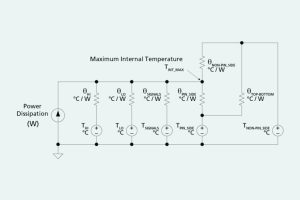
Figure 3: BCM6135 two-sided cooling thermal resistance model using electrical element
equivalence.

Figure 4: BCM6135 two-sided annotated thermal resistance model with element value annotation.
Estimation of internal module temperature profile
The thermal capacitance is used to calculate the thermal time constant of the module during a transient thermal event. This time constant is the product of thermal capacitance and thermal resistance. The value given for thermal capacitance in product datasheets is a calculated value that assumes the product is at a uniform temperature internally (throughout the module) at all times during the transient thermal event. This is a linearized simplification, but it allows the product designer a method to quickly estimate the temperature-versus-time behavior of the product early in the product design cycle. The simplification of uniform internal temperature also implies that the thermal time constant better reflects actual product performance when utilized for double-sided cooling of the 48V power module using heat sinks.
For example, an equivalent circuit to model the thermal resistance of the BCM6135 is shown in Figure 5. Electrical resistors are analogous to thermal resistances in units of degrees Celsius per watt [°C/W]. A current source is analogous to a heat source in units of watt [W]. A voltage source is analogous to a temperature source in this circuit model with units of degrees Celsius [°C].
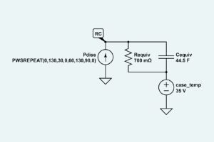
Figure 5: BCM6135 thermal model equivalent electrical circuit assumes package top and bottom cooling with an equivalent thermal resistance of 0.7°C/W and case temperature of 35°C.
The equivalent circuit assumes package top and bottom cooling with an equivalent thermal resistance of 0.7°C/W and case temperature of 35°C, thermal capacitance of the module of 44.5J/K, and that the module dissipates 130W during 30 seconds-on, 30 seconds-off continuously repeated pulses.
Simulation results for this circuit are shown in Figure 6; the operating conditions are 520 VHI, 32.5 VLO, 80A low-side peak output current (2.6kW peak output power). During the first power pulse, the maximum internal temperature increases to about 90°C. The next pulse shows an increase in maximum internal temperature to about 115°C. Repeated pulses would show maximum internal temperature remains around 115°C.
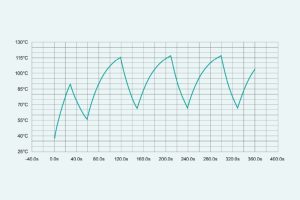
Figure 6: Simulated BCM pulsed power thermodynamics under the operating conditions 520 VHI, 32.5 VLO, 80A low-side peak output current. First power pulse shows the maximum internal temperature increases to about 90°C, followed by an increase to about 115°C. Repeated pulses would show maximum internal temperature limits to about 115°C.
Application testing of the module should always be conducted to validate initial modeled estimates of transient performance and to properly design a passive convective heatsink.
Lab test results
The BCM6135 is inherently bidirectional with instantaneous switching of the directional mode of operation. The conversion efficiency of the module is the same regardless of the direction of current flow.
In the regenerative active suspension application, the 800V battery is sourcing current when the vehicle is traveling over smooth road surfaces and the suspension actuation motor is the 48V load. When a pothole is encountered by the vehicle, the motors in the suspension momentarily become generators (compression), and the voltage on the low side of the BCM increases above the voltage of the 800V battery divided by the conversion K factor (K = 1/16 in this application). This difference in potential causes the bus converter to swap the direction of current flow, without internal loop controller intervention. The 800V battery then momentarily becomes the load (rebound) and recovers energy by charging through its battery management system circuit.
Once the displacement from the pothole has subsided, the bus converter will once again step down the 800V battery and supply current to the suspension linear motors. All of this occurs without intervention by the vehicle’s on-board processors. The frequency of these suspension actuations ranges from about 1Hz to 10Hz. Interestingly, the road surface profile is essentially an analog of the bus converter load step dynamics.
It is the potential difference between the bus converter high and low sides that defines the current amplitude and direction.
Imagine that the load on the low side is a passive load (such as a resistor) and on the high side there is a battery with a potential of 800V. The BCM will act as a K = 1/16 voltage transformer and create a potential on the low side equal to 50V. Current will flow through that resistor and is determined by voltage applied across the resistor.
If an energy source is added to the low side with potential of 51V and replaces the resistor, the potential difference between the output of BCM (50V) and that energy source (51V) will be negative (–1V), and the current will start flowing in the opposite direction. The level of this current will be defined by the total path resistance inside the BCM and the battery.
This can be visualized with the BCM connected to 800V source on the high side and a bidirectional power supply on the low side. By varying the voltage on the bidirectional power supply ±100mV, current will flow alternatively in both directions, and the peak current will be 100mV divided by the BCM output resistance. For a bus converter output impedance of 25mΩ, this yields a peak current of approximately 4A flowing bidirectionally under these assumptions (Figure 7).
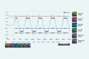
Figure 7: Oscilloscope screen capture of bus converter bidirectional current flow by varying the voltage on the bidirectional power supply ±100mV, current will flow alternatively in both directions, and the peak current will be 100mV divided by the BCM output resistance. The bus converter output impedance might be typically 25mΩ, so this yields a peak current of approximately 4A flowing bidirectionally under these assumptions.
In lab tests (Figure 8), the BCM6135 has demonstrated peak power of 4kW (80A at 50V) for 60ms, an indicator that the module design is thermally robust across dynamic loads.
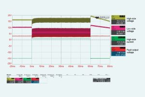
Figure 8: Oscilloscope screen capture – 4kW for 60ms. In lab tests the BCM6135 has demonstrated peak Power of 4kW (80A at 50V) for 60ms, an indicator that the module design is thermally robust across dynamic loads.
In a second lab test (Figure 9), the load was pulsed from 16A to 80A with a 10% duty cycle (900ms at 16A and 100ms at 80A). The operating condition is 520VHI and 32.5VLO; this is the low end of the supported BCM6135 voltage range. The average power delivery was 720W (22A at 32.5V). Over the course of 30 minutes (1800s), the internal sensor “read temperature” (a proxy for junction temperature) indicated a steady-state temperature of ~100°C, considerably below the maximum allowable junction temperature of 125°C. The test setup was passive cooling with a single-sided heat sink. This is another positive indicator for the targeted passively cooled application.
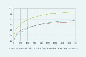
Figure 9: 10% duty cycle 16A to 80A load step with 100°C steady-state read temperature after 1800 seconds (with single-sided heat sink).
On the other hand, in a third lab test (see Figure 10), with the same thermal management setup, the average power delivery was increased to 1.1kW (22A at 50V). In this test, the operating condition is 800VHI and 50VLO; this is the high end of the supported BCM6135 voltage range. The load was pulsed from 17.5A to 70A with a 10% duty cycle (900ms at 17.5A and 100ms at 70A). In 7.5 minutes, the sensed internal temperature was 100°C and was still rising (not in steady state). But 7.5 minutes (450 seconds) is a much longer duration than 20 seconds, so this is a positive indicator that the BCM6135 may meet some active suspension design requirements.
Ultimately, the BCM6135 was lab characterized to support an average power of 1.3kW for 30 seconds with a passively-cooled heat sink across the sealed-enclosure operating temperature range.
Active suspension design objectives include road surface profile assumptions (amplitude and duration of bumps and holes that can be mitigated), and these assumptions bear directly on the required peak power capability of the DC-DC converter. The electromagnetic characteristics of the linear motor also impact the DC-DC converter requirements. That said, the BCM6135 is an indispensable bus converter module for contemporary active suspension, active anti-roll control DC-DC converter subsystems.
Conclusion
The economic and quality-of-life benefits of electrification is driving the adoption of HV to 48V DC-DC conversion across equipment types throughout the global economy. Integrated high-voltage to 48V power modules are becoming more common in EVs and HEVs as battery voltages increase and 48V low voltage buses become more widespread.
Next-generation bidirectional fixed-ratio bus converter modules are capable of meeting electrically and thermally demanding requirements in transient regenerative use case applications such as active electric vehicle suspensions. The passively cooled findings presented are significant in light of the accelerating trend towards more costly liquid-cooled power delivery systems.
The post High-voltage bus converter power modules for electric vehicle 48V power delivery networks appeared first on ELE Times.
Microchip Enhances TrustMANAGER Platform to Support CRA Compliance and Cybersecurity Regulations
International cybersecurity regulations continue to adapt to meet the evolving threat landscape. One major focus is on outdated firmware in IoT devices, which can present significant security vulnerabilities. To address these challenges, Microchip Technology is enhancing its TrustMANAGER platform to include secure code signing and Firmware Over-the-Air (FOTA) update delivery as well as remote management of firmware images, cryptographic keys and digital certificates. These advancements support compliance with the European Cyber Resilience Act (CRA) which mandates strong cybersecurity measures for digital products sold in the European Union (EU). Aligned with standards like the European Telecommunications Standards Institute (ETSI) EN 303 645 baseline requirements of cybersecurity for consumer IoT and the International Society of Automation (ISA)/International Electrotechnical Commission (IEC) 62443 security of industrial automation and control systems standards, the CRA sets a precedent that is expected to influence regulations worldwide.
Microchip’s ECC608 TrustMANAGER leverages Kudelski IoT’s keySTREAM Software as a Service (SaaS) to deliver a secure authentication Integrated Circuit (IC) that is designed to store, protect and manage cryptographic keys and certificates. With the addition of FOTA services, the platform helps customers securely deploy real-time firmware updates to remotely patch vulnerabilities and comply with cybersecurity regulations.
“As evolving cybersecurity regulations require connected device manufacturers to prioritize the implementation of mechanisms for secure firmware updates, lifecycle credential management and effective fleet deployment,” said Nuri Dagdeviren, corporate vice president of Microchip’s security products business unit. “The addition of FOTA services to Microchip’s TrustMANAGER platform offers a scalable solution that removes the need for manual, and expensive, static infrastructure security updates. FOTA updates allow customers to save resources while fulfilling compliance requirements and helping to future-proof their products against emerging threats and evolving regulations.”
Further enhancing cybersecurity compliance, the Microchip WINCS02PC Wi-Fi network controller module used in the TrustMANAGER development kit is now certified against the Radio Equipment Directive (RED) for secure and reliable cloud connectivity. RED establishes strict standards for radio devices in the EU, focusing on network security, data protection and fraud prevention. Beginning August 1, 2025, all wireless devices sold in the EU market must adhere to RED cybersecurity provisions.
By incorporating these additional services, TrustMANAGER—governed by keySTREAM—tackles key challenges with IoT security, regulatory compliance, device lifecycle management and fleet management. This solution is designed to serve IoT device manufacturers and industrial automation providers.
Development Tools
The ECC608 TrustMANAGER is compatible with the MPLAB X Integrated Development Environment (IDE) and supported by Microchip’s CryptoAuth PRO development board (EV89U05A) and the CryptoAuthLib software library. The Trust Platform Design Suite (TPDS) contains a use case example including onboarding educational steps and a firmware code example to enable the keySTREAM service to AWS with the ECC608 secure element running on a 32-bit Arm Cortex-M4-based PIC32CX SG41MCU and a WINCS02PC Wi-Fi module.
The post Microchip Enhances TrustMANAGER Platform to Support CRA Compliance and Cybersecurity Regulations appeared first on ELE Times.
EEVblog 1692 - $130 Fluke 17B MAX Multimeter REVIEW
Farads
 | submitted by /u/Linker3000 [link] [comments] |
Take back half improves PWM integral linearity and settling time

PWM is a simple, cool, cheap, cheerful, and (therefore) popular DAC technology. Excellent differential nonlinearity (DNL) and monotonicity are virtually guaranteed by PWM. Also guaranteed are a stable zero and a full-scale accuracy that’s generally limited only by the quality of the voltage reference. However, PWM’s integral nonlinearity (INL) isn’t always terrific, and the necessity for low-pass filtering-out of ripple means its speed isn’t too swift either. These messy topics are covered in…
- A common cause of, and a software cure for, PWM INL is discussed here in “Minimizing passive PWM ripple filter output impedance: How low can you go?”
- The slow PWM settling times (Ts) that can be problematic, together with a way to reduce them, are addressed here in “Cancel PWM DAC ripple with analog subtraction.”
Figure 1 offers a tricky, totally analog strategy for both. The ploy in play is Take Back Half (TBH). It relies on two differential relationships that effectively subtract (take back) the error terms.
- For signal frequencies less than or equal to 1/Ts (including DC) Xc >> R and Z = 2(Xavg – Yavg/2).
- For frequencies greater than or equal to Fpwm, Xc << R and Z = Xripple – Yripple.

Figure 1 All Rs and Cs are nominally equal. The circuit relies on two differential relationships that effectively subtract the error terms for the TBH methodology.
Wow the engineering world with your unique design: Design Ideas Submission Guide
Because only one switch drives load R at node Y while two in parallel drive X, INL due to switch loading at Y is exactly twice that at X. Therefore, Z = 2(Xavg – Yavg/2) takes back, cancels the error, and has (theoretically) zero INL.
Xripple = Yripple, so Z = Xripple – Yripple = 0 nulls it out, has likewise (theoretically) zero ripple, and ripple filter RC time constants can be made faster and settling times shorter.
The DC conversion component at Z = -PWM_duty_factor * Vref. Conversion accuracy is precisely unity, independent of resistance and capacitance tolerances. However, they ideally should be accurately equal for best ripple and nonlinearity cancellation.
Stephen Woodward’s relationship with EDN’s DI column goes back quite a long way. Over 100 submissions have been accepted since his first contribution back in 1974.
Related Content
- Minimizing passive PWM ripple filter output impedance: How low can you go?
- Cancel PWM DAC ripple with analog subtraction
- Temperature controller has “take-back-half” convergence algorithm
- 20MHz VFC with take-back-half charge pump
- Take-Back-Half precision diode charge pump
The post Take back half improves PWM integral linearity and settling time appeared first on EDN.
ELENA project develops Europe’s first LNOI substrates for photonic integrated circuits, completing supply chain
Засідання Наглядової ради проєкту «Коаліція укриттів цивільного захисту»

На заході обговорювалися подальші кроки щодо розвитку мережі укриттів по всій території України і були присутні представники України та Фінляндії:
EPC Space launches 300V rad-hard GaN FET
Silvaco and Fraunhofer ISIT collaborate on developing GaN device technology
XVI Міжнародна конференція "Інновації молоді в машинобудуванні"

XVI Міжнародна науково-технічна конференція молодих вчених та студентів "Інновації молоді в машинобудуванні", що відбулась у змішаному форматі (очно та онлайн) у Державному політехнічному музеї КПІ ім. Ігоря Сікорського, мала широку тематику доповідей.
MIT-led team develops low-cost, scalable process for integrating GaN transistors onto silicon CMOS chips
Made a non contact thermometer with a stm32 powering it and lots of gpio pins
 | Features [link] [comments] |
PhotonDelta and Luminate NY collaborate on transatlantic growth network for photonics startups
CSA Catapult to mobilize new UK Semiconductor Centre
New EDA tools arrive for chiplet integration, package verification

The world we are living in is increasingly becoming software-defined, where artificial intelligence (AI) is adding the next layer of functionality. And it’s driving the need for more compute to enable the software-enabled functionality. However, with this huge progression in compute content, Moore’s Law scaling will be insufficient to support the number of transistors for the needed compute.
Enter 3D ICs, disaggregating the functionality of silicon into a set of chiplets and then heterogeneously integrating them on an advanced integration platform. “Hyperscalers, driving the compute envelope, are particularly pushing the extreme where 3D ICs are needed,” said Michael White, VP of Calibre Design Solutions at Siemens EDA.
White also noted automotive designs where self-driving technology content is driving the need for 3D ICs. At the Design Automation Conference (DAC) held in San Francisco, California, on 22-25 June 2025, Siemens EDA announced two key additions to its EDA portfolio to address and overcome the complexity challenges associated with the design and manufacture of 2.5D and 3D IC devices.
First, the company’s Innovator3D IC suite enables chip designers to efficiently author, simulate, and manage heterogeneously integrated 2.5D and 3D IC designs. Second, its Calibre 3DStress software leverages advanced thermo-mechanical analysis to identify the electrical impact of stress at the transistor level.

Figure 1 The new tools aim to dramatically reduce risk and enhance the design, yield, and reliability of complex, next-generation 2.5D/3D IC designs. Source: Siemens EDA
“These solutions help designers achieve the needed compute performance while increasing yield and reliability and reducing cost,” White added. “They also offer the ability to leverage higher bandwidth between the chiplets placed on an interposer.” He calls this an inflection point in the design process and tools needed for the design flows.
Chiplet integration with Innovator3D IC
Keith Felton, principal technical product manager for 3D IC solutions at Siemens EDA, expanded on 3D IC being an inflection point, marking a transition from single design-centric approach to system-centric approach. “It impacts design flows and tools, necessitating a system-centric approach from early planning through final sign-off in four ways,” he added.
First, chip designers need system floor planning to optimize power, performance, area, and reliability across silicon, package, interposer, and even PCB. Second, they must start using multi-physics modeling to simulate complex thermo-mechanical interactions that impact electrical and structural performance.
Third, IC designers need to have a methodology for scalability to manage and communicate heterogeneous data across enterprise-wide teams and maintain digital continuity because there are hundreds of silicon designs encompassing chiplets. Fourth, designers must have a methodology for multi-die sign-off, enabling 3D verification of connectivity, interfaces, interconnect reliability, and electrostatic discharge (ESD) resiliency.
So, Innovator3D IC suite provides a fast, predictable path for planning and heterogeneous integration, substrate/interposer implementation, interface protocol analysis compliance and data management of designs, and design data IP.

Figure 2 Innovator3D IC suite facilitates design, verification, and data management of 2.5D and 3D IC chiplets. Source: Siemens EDA
Innovator3D IC—comprising four building blocks—offers an AI-infused user experience with extensive multithreading and multicore capabilities to achieve optimal capacity and performance on 5+ million pin designs. First, Innovator3D IC Integrator comes with a consolidated cockpit for constructing a digital twin, using a unified data model for design planning, prototyping, and predictive analysis.
Second, Innovator3D IC Layout facilitates correct-by-construction package interposer and substrate implementation. Third, Innovator3D IC Protocol Analyzer can be used for chiplet-to-chiplet and die-to-die interface compliance analysis. It’ll be critical in ensuring compliance with protocols such as Universal Chiplet Interconnect Express (UCIe). Finally, the Innovator3D IC Data Management part is targeted at the work-in-progress management of designs and design data IP.
“Innovator3D IC is targeting the optimization of 2.5 and 3D IC design performance to eliminate late-stage changes by enabling early prototyping and planning,” Felton said. “It accelerates compliance with protocols for chiplet integration and provides a core workflow that design teams need for 3D IC chiplet integration.”
Calibre 3DStress for package verification
Calibre 3DStress—the second part of Siemens EDA’s solution to streamline the design and analysis of complex, heterogeneously integrated 3D ICs—supports accurate, transistor-level analysis, verification, and debugging of thermo-mechanical stresses and warpage in the context of 3D IC packaging.
It enables IC designers to assess how chip-package interaction will impact the functionality of their designs earlier in the development cycle. Shetha Nolke, principal product manager for Calibre 3DStress at Siemens EDA, told EDN that this tool performs three key tasks for chip-package stress analysis in 3D IC designs.
First, stress simulation ensures accurate die levels under thermal and mechanical conditions. Second, what-if analysis optimizes IP, cell, or chip placement during early design stages. Third, it performs stress-aware circuit analysis using back annotation of device stress to minimize electrical impact.

Figure 3 With the thinner dies and higher package processing temperatures of 2.5D/3D IC architectures, designers often discovered that designs validated and tested at the die level no longer conform to specifications after packaging reflows. Source: Siemens EDA
3D ICs increasingly face stress- and warpage-related packaging challenges. That includes thermal challenges such as non-uniform heat generation and dissipation, which can result in higher temperatures and temperature gradients. Then, there are thermo-mechanical issues, where packaging process stages experience high temperature and fixed constraints.
Finally, thinned dies and ultra-low-k dielectrics increase mechanical stress-induced problems. “As multiple chiplets are integrated into a package, they experience thermal impacts because heat is not able to escape readily,” Nolke said. “While mechanical aspects are coming from incorporating package components, Calibre 3DStress can model it before fabrication.”
Calibre 3DStress delivers accurate die-level stress simulation using finite element analysis at a nano-meter feature scale. It also provides visualization of stress and warpage results while facilitating electrical and mechanical verification.
Related Content
- TSMC, Arm Show 3DIC Made of Chiplets
- One-stop advanced packaging solutions for chiplets
- Cadence to Buy Artisan to Support Chiplet, 3D IC Future
- Cadence enables multi chiplet design with Integrity 3D-IC platform
- Advanced IC Packaging: The Roadmap to 3D IC Semiconductor Scaling
The post New EDA tools arrive for chiplet integration, package verification appeared first on EDN.
Фінансування престижного міжнародного конкурсу Erasmus+ для проекту кафедри ХТФ

Кафедра Технології неорганічних речовин, водоочищення та загальної хімічної технології разом з партнерами із 9 університетів Норвегії, Румунії, Молдови, Сербії та України отримали фінансування престижного міжнародного конкурсу Erasmus+ із проєктом DIGISKILLS («Посилення цифрових навичок у водному секторі вищої освіти»).
DIY isolation transformer enhances Bode analysis with modern DSOs
Keysight, Teledyne LeCroy, Tektronix, Rohde & Schwarz (R&S), and others have offered built-in digital oscilloscope Bode analysis for some time, and this feature has trickled down to low-cost DSOs like the Siglent SDS2000X Plus and the new SDS814X HD. These DSOs feature built-in Bode analysis when operating with a companion AWG, or sometimes include the AWG within (SDS2000X Plus), at an affordable price point.
Wow the engineering world with your unique design: Design Ideas Submission Guide
DIY common-mode chokeOne of the interesting applications of this Bode capability is investigating the open-loop response of closed-loop systems, such as oscillators. This often requires an expensive isolation transformer, which can be limiting. However, for those with a DIY spirit, a reconfigured common-mode choke serves as a nice isolation transformer for Bode analysis (Figure 1) [1].
![]() Figure 1 A reconfigured common-mode choke isolation transformer used to investigate the open-loop response of closed-loop systems, e.g., oscillators, using the Bode capability of a benchtop oscilloscope.
Figure 1 A reconfigured common-mode choke isolation transformer used to investigate the open-loop response of closed-loop systems, e.g., oscillators, using the Bode capability of a benchtop oscilloscope.
Creating the isolation transformer is straightforward. Physically larger common-mode “chokes” utilized in AC mains, like the one shown, make good candidates, especially for lower frequencies.
Here, 5 mH and 2 mH Prod Tech PDMCAT221413 types were utilized after unwinding and rewinding. First, after the unwinding, the pair of wires are stretched, and then the pair of wires are twisted together (a hand drill helps). This leaves a long twisted pair which is threaded through the core as many times as possible.
As shown in Figure 2, the wrapped core now has two ends with the twisted pair, and at each end, a pair of wires. The ends of the wire on each side are common with the other pair of wires’ ends (use an ohmmeter), becoming the primary or secondary. Either way, it doesn’t matter since the isolation transformer has a 1:1 turns ratio and is symmetrical. The primary and secondary can be resistively terminated as needed for specific applications.
![]()
Figure 2 A side-view of the DIY isolation transformer showing the wrapped core and terminated with four 2-W, 100-Ω resistors.
Figure 3 shows the test setup utilizing the DIY isolation transformer to measure the open-loop response of a Peltz oscillator, as described in another Design Idea (DI): “Simple 5-component oscillator works below 0.8V.”
![]()
Figure 3 Test setup using the DIY isolation transformer to measure the open-loop response of a Peltz oscillator.
Peltz oscillator test circuit and resultsThe isolation transformer secondary is connected between Q2 base and Q1 collector. Q1 and Q2 are 2N3904s, L is 470 µH, C is 0.022 µF, and R is 510 Ω (Figure 4).
![]()
Figure 4 The configuration of the Peltz oscillator circuit, where the isolation transformer is connected between Q2 base and Q1 collector to measure open-loop response.
For comparison, an LTspice circuit model was created. The simulated and measured results using the SDS2504X Plus are shown in Figure 5.
![]() Figure 5 Simulated (top) and measured (bottom) results with the circuit under test in Figure 4 operating with the following values: L is 470 µH, C is 0.022 µF, and R is 510 Ω.
Figure 5 Simulated (top) and measured (bottom) results with the circuit under test in Figure 4 operating with the following values: L is 470 µH, C is 0.022 µF, and R is 510 Ω.
Changing the inductor to 100 µH (measured 97.3 µH) which moves the center frequency to 34.4 kHz (Figure 6).
![]()
Figure 6 Simulated (top) and measured (bottom) results with the circuit under test in Figure 4 operating with the following values: L is 100 µH, C is 0.022 µF, and R is 510 Ω.
Typically, physically larger common-mode chokes have higher inductance, which can extend the measurement range to lower frequencies. Having a larger core also allows for more turns, which also helps with lower frequencies.
However, larger cores and more turns limit the upper frequency end, and having more cores, smaller and larger, can cover a wider frequency range than a single-core transformer. I’ve had good results with the cores shown from less than 100 Hz to over 1 MHz.
This is just one of the many uses for modern Bode-enabled DSOs with companion AWGs and a few DIY isolation transformers.
Michael A Wyatt is a life member with IEEE and has continued to enjoy electronics ever since his childhood. Mike has a long career spanning Honeywell, Northrop Grumman, Insyte/ITT/Ex-elis/Harris, ViaSat and retiring (semi) with Wyatt Labs. During his career he accumulated 32 US Patents and in the past published a few EDN Articles including Best Idea of the Year in 1989.
Related Content
- Simple 5-component oscillator works below 0.8V
- Injection locking acts as a frequency divider and improves oscillator performance
- Investigating injection locking with DSO Bode function
- DIY custom Tektronix 576 & 577 curve tracer adapters
References
The post DIY isolation transformer enhances Bode analysis with modern DSOs appeared first on EDN.
Питання інженерії поверхні в авіадвигунобудуванні держава визнає серед найактуальніших

У відповідь на сучасні виклики та запити українського суспільства, а також задля забезпечення конкурентоспроможності України у світі, сприяння розвитку національного дослідницького потенціалу й інтеграцію до світового дослідницького простору, МОН проводить конкурси серед науковців з подальшим наданням фінансування на виконання передових фундаментальних досліджень, які передбачають постановку і розв'язання актуальних наукових проблем. "Київський політехнік" продовжує знайомити читачів з проєктами науковців нашого університету, що цього року отримали державне фінансування. Серед них – розробка дослідників НН ІМЗ ім. Є.О.Патона.
TNO to construct InP-based photonic chip pilot manufacturing line
EPC releases compact, high-efficiency 180W GaN buck converter evaluation board for USB PD applications
Pages

