
Feed aggregator
GMSL video link’s quest to become open automotive standard

The Gigabit Multimedia Serial Link (GMSL) technology of Analog Devices Inc. (ADI) is finally heading down the standardization path with the inception of the OpenGMSL Association, a non-profit entity joined by an automotive OEM, tier 1 suppliers, semiconductor companies, and several test and measurement firms.
GMSL—a SerDes technology for automotive applications like advanced driver assistance systems (ADAS), touchscreen infotainment, and in-vehicle connectivity—facilitates high-resolution video links while supporting data transfer speeds of up to 12 Gbps. ADI claims to have shipped more than 1 billion GMSL chips for automotive-grade platforms.

Figure 1 GMSL is a point-to-point serial link technology dedicated to video data transmission; it was originally designed for automotive camera and display applications. Source: ADI
OpenGMSL Association aims to turn this automotive SerDes technology into an open standard for in-vehicle connectivity. “As automotive architectures evolve to meet the growing demands of in-vehicle communication, networking and data transfer, it is critical that the industry has access to open global standards such as OpenGSML to enable ecosystem-led innovation,” said Fred Jarrar, VP and GM of Power and ASIC Business Unit at indie Semiconductor, a member of OpenGMSL Association.
Among the test and measurement companies joining the OpenGMSL Association are Keysight Technologies, Rohde & Schwarz, and Teledyne LeCroy. These in-vehicle network test outfits will help OpenGMSL in facilitating the development and deployment of interoperable and reliable automotive systems through a standardized, open ecosystem for in-vehicle connectivity.
Hyundai Mobis, which has used the GMSL technology in the Korean OEM’s vehicles for many years, has also joined the initiative to standardize GMSL. Then, there is GlobalFoundries (GF), pitching its 22FDX, 12LP+ and 40LP process technologies for GMSL chips targeted at next-generation automotive applications.

Figure 2 OpenGMSL aims to transform SerDes transmission of video and/or high-speed data as an open standard across the automotive ecosystem. Source: ADI
Next-generation automotive platforms like ADAS heavily rely on high-quality video data to make critical, real-time decisions that improve driver safety and reduce accidents. Likewise, touchscreen infotainment systems demand high-speed and low-latency connectivity for seamless, immersive user experiences.
OpenGMSL aims to accelerate innovation across these automotive platforms by cultivating a standardized, open ecosystem for in-vehicle connectivity. ADI is betting that an open standard for video and/or high-speed data transmission built around its GMSL technology will bolster autonomous driving, ADAS, and infotainment applications, and its own standing in the automotive market.
Related Content
- Machine-Vision Architectures for Automotive Apps
- ADI’s GMSL technology eyes a place on ADAS bandwagon
- Using GMSL SerDes Devices in a Dual Automotive (ECU) Application
- Complex but necessary technology for automotive: Serial links re-visited
The post GMSL video link’s quest to become open automotive standard appeared first on EDN.
Power amplifiers that oscillate—deliberately. Part 1: A simple start.

Editor’s Note: This DI is a two-part series.
In Part 1, Nick Cornford deliberately oscillates the TDA7052A audio power amplifier to produce a siren-like sound and, given the device’s distortion characteristics, a functional Wien bridge oscillator.
In Part 2, Cornford minimizes this distortion and adds amplitude control to the circuit.
When audio power amplifiers oscillate, the result is often smoke, perhaps with a well-cooked PCB and a side order of fried tweeter. This two-part Design Idea (DI) shows some interesting ways of (mis-)using a common power amp to produce deliberate oscillations of varying qualities.
That device is the TDA7052A, a neat 8-pin device with a high, voltage-controllable gain, capable of driving up to a watt or so into a bridge-tied load from its balanced outputs. The TDA7056A is a better-heatsinked (-heatsunk?) 5-W version. (That “A” on the part number is critical; the straight TDA7052 has slightly more gain, but no control over it.) The TDA7052B is an uprated device with a very similar spec, and the TDA7056B is the 5-W counterpart of that. But now the bad news: they are no longer manufactured. Some good news: they can easily be found online, and there is also a Taiwanese second source (or clone) from Unisonic Technologies Ltd.
A simple circuit’s siren song
For the best results, we’ll need to check out some things that don’t appear on the data sheets, but let’s cut straight to something more practical: a working circuit. Figure 1 shows how the balanced, anti-phase outputs help us build a simple oscillator based on the integrator-with-thresholds architecture.
Figure 1 A minimalist power oscillator, with typical waveforms.
This circuit has just three advantages: it’s very simple, reasonably efficient, and, with a connected speaker, very loud. Apart from those, it has problems. Because of the amp’s input loading (nominally 20k) and the variation of drive levels with different loads, it’s hard to calculate the frequency precisely. (The frequency-versus-R1 values shown are measured ones.) R2 is needed to reduce loading on the timing network, but must leave enough gain for steady operation. (A series capacitor here proved unnecessary, as the internally biased input pin is being over-driven.) Its efficiency is due to the amp’s output devices being run in saturation: with no extra heatsinking, the (DIL-8) package warms by ~15°C when driving into an 8 Ω speaker. The square wave produced is somewhat asymmetrical, though good enough for alarm use.
Figure 1 shows a 5-V supply. Raising that to 12 V made only one change to the performance: the output became very, very loud. And it drew around an amp with a 10 Ω load. And it could do with a heatsink. And a TDA7056A/B rather than a ’52.
The Vcon input on pin 4 is not used. Left open, it floats at ~1.14 V, giving the device a measured gain of around 25 dB. Taking it close to ground inhibits operation, so a bare-drain MOSFET hooked on here can give on/off control. Taking it higher gives full gain, with a shift in frequency. If that is not important (and, in this context, why should it be?), logic control through a 22k resistor works fine. When inhibited, the device still draws 8–10 mA.
Feeding Vcon with varying analog signals of up to a few tens of hertz can produce interesting siren effects because changes in gain affect the oscillation frequency. But for a proper siren, it would be better to generate everything inside a small micro and use an H-bridge of (less lossy) MOSFETs to drive the speaker with proper square waves. (We’ve all heard something like that on nearby streets, though hopefully not in our own.)
Fancy sound effects apart, any power amp with a suitable input structure, enough gain, and balanced (BTL) outputs should work well in this simplest of circuits.
Determining distortion
So much for simplicity and raw grunt. Now let’s take a look at some of the device’s subtleties and see how we can use those to good effect. Distortion will be critical, but the data sheet merely quotes 0.3 to 1% under load, which is scarcely hi-fi. If we remove the load, things look much healthier. Figure 2 shows the unloaded output spectrum when the input was driven from an ultra-low-distortion oscillator, at levels trimmed to give 0 dBu (2.83 V pk-pk) and -20 dBu at the output with a device gain fixed at around 25 dB (Vcon was left open, but decoupled).

Figure 2 The TDA7052A’s output spectra for high and low output levels, taken under ideal conditions and with no output load.
Further tests with various combinations of input level and device gain showed that distortion is least for the highest gains—or smallest gain-reductions—and lowest levels. With outputs less than ~300 mVpk–pk (~-18 dBu) and gains more than 10 dB, distortion is buried in the noise.
That’s unloaded. Put a 10 Ω resistive load across the outputs, and the result is Figure 3.

Figure 3 Similar spectra to Figure 2, but with a 10-Ω output load.
That looks like around -38 dB THD for each trace, compared with better than -60 and -70 dB for the unloaded cases. All this confirms that the distortion comes mainly from the output stages, and then only when they are loaded.
A working one-chip sine-wave oscillator—
This means that we have a chance to build a one-chip Wien bridge audio oscillator, which could even drive a power load directly while still having lower distortion than the average loudspeaker. Let’s try adding a Wien frequency-selective network and a simple gain-control loop, which uses Zener diodes to sense and stabilize the operating level, as in Figure 4.

Figure 4 A simple gain control loop helps maintain a constant output amplitude in a basic Wien bridge oscillator.
The Wien network is R1 to R4 with C1 and C2. This has both minimum loss (~10 dB) and minimum phase shift (~0°) at f = 1 / 2π C2 (R2 + R4), which gives the oscillation frequency when just enough positive feedback is added. When the amplitude is large enough, Zeners D1 and D2 start to conduct on the peaks, progressively turning Q1 on, thus pulling U1’s Vcon pin lower to reduce its gain enough to maintain clean oscillation.
C3 smooths out the inevitable ripple and determines the control loop’s time-constant. R5 minimizes U1’s loading of the Wien network while C3 blocks DC, and R6 sets the output level. The unloaded spectra for outputs of 0 and -10 dBV are shown in Figure 5.
 Figure 5. The spectra of Figure 4’s oscillator for 0 and -10 dBV outputs with no load.
—that has problems
While those spectra are half-decent, with THDs of around -45 and -60 dB (or ~0.1% distortion), they are only valid for a given temperature and with no extra load on the output. Increasing the temperature by 25°C halves the output amplitude—no surprise, given the tempcos of the diodes and the transistor. And those 3.3-V Zeners have very soft knees, especially at low operating currents, so they are better regarded as non-linear resistors than as sharp level-sensors.
Adding a 10-Ω resistor as a load—and tweaking R6 to readjust the levels—gives Figure 6.

Figure 6 Similar spectra to Figure 5’s but with the output loaded with 10 Ω.
THD is now around -30 dB, or 3%. Unimpressive, but comparable with many speakers’ distortions, and actually worse than the data-sheet figures for a loaded device.
So, we must conclude that while a one-chip sinusoidal oscillator based on this is doable, it isn’t very usable, and further tweaks won’t help much. We need better amplitude control, which means adding another chip, perhaps a dual op-amp, and that is what we will do in Part 2.
—Nick Cornford built his first crystal set at 10, and since then has designed professional audio equipment, many datacomm products, and technical security kit. He has at last retired. Mostly. Sort of.
Related Content
- Ultra-low distortion oscillator, part 1: how not to do it.
- Ultra-low distortion oscillator, part 2: the real deal
- Distortion in power amplifiers, Part IV: the power amplifier stages
- A pitch-linear VCO, part 1: Getting it going
- A pitch-linear VCO, part 2: taking it further
The post Power amplifiers that oscillate—deliberately. Part 1: A simple start. appeared first on EDN.
Network Traffic Analysis of NoFilter GPT: Real-Time AI for Unfiltered Conversations
NoFilter GPT is a cutting-edge conversational AI built to deliver unfiltered, bold, and authentic interactions. It offers different modes for different tasks: Raw Mode delivers candid, no-nonsense dialogue; Insight Mode explores complex topics with sharp analysis; and Reality Check Mode debunks misinformation with brutally honest takes. NoFilter GPT is designed for users who value clarity, directness and intellectual integrity in real-time conversations.
Network Traffic AnalysisThe ATI team in Keysight has analyzed the network traffic of NoFilter GPT and found some interesting insights that can help researchers optimize performance and enhance security. This analysis was conducted using HAR captures from a web session. NoFilter GPT operates with standard web protocols and relies on secure TLS encryption for communication.
Overall AnalysisWe have performed extensive user interactions with the NoFilter GPT web application. The captured traffic was completely TLS encrypted. We have further analyzed the traffic based on host names.

Figure 1: Request-Response count per host
In the figure above we can observe the majority of request-response interactions were observed with nofiltergpt.com, handling core AI functions like chat and image generation. Additionally, NoFilterGPT related host, chat.nofiltergpt.com manage AI chat, image generation, and token-based request authentication, while other external hosts primarily serve static assets and analytics.

Figure 2: Cumulative payload per host
The diagram above shows that the host chat.nofiltergpt.com has the maximum cumulative payload followed by nofiltergpt.com. The rest of the hosts are creating smaller network footprints.
Analyzing EndpointsBy examining the HAR file, we gain a detailed view of the HTTP requests and responses between the client and NoFilter GPT’s servers. This analysis focuses on critical endpoints and their roles in the platform’s functionality.
Chat CompletionEndpoint: https://chat.nofiltergpt.com/run/nofilterai/controller5?identifier…
- Method: POST
- Purpose: This is the actual request that sends user input to the chat model and receives a response.
- Request Headers:
- Content-Type: application/json
- Accept: */* (Accepts any response type, indicating a flexible API for logging events.)
- Origin: https://nofiltergpt.com (Ensures requests originate from NoFilterGPT’s platform)
- Request Payload: Base64-encoded JSON containing user message, system prompt, temperature, etc.
- Response Status: 200 OK (successful session creation)
This triggers a response from the model.
- Method: OPTIONS
- Purpose: This is a CORS ( Cross-Origin Resource Sharing ) preflight request automatically sent by the browser before the POST request.
- Request Payload: None
The server responds with headers indicating what methods and origins are allowed, enabling the browser to safely send the POST.
Image Generation- Endpoint: https://chat.nofiltergpt.com/media/generate2.php

- Method: POST
- Purpose: Sends an image generation prompt to the server.
- Request Headers:
- Content-Type: application/json
- Accept: */* (Accepts any response type, indicating a flexible API for logging events.)
- Request Payload: JSON with token, prompt, width, height, steps, sampler, etc.
- Response Status: 200 OK (successful session creation)
This generates and returns an image based on the prompt and settings.

- Method: OPTIONS
- Purpose: Browser-initiated CORS preflight checks to see if the server will accept the POST request
- Request Payload: None
Gets permission from the server to proceed with the actual POST request.
NOTE: While NoFilterGPT can be useful it is a prohibited tool by many companies and government entities. Policy and technical systems must be in place to prevent usage, and it is vital to confirm this via test using BreakingPoint. These tests help validate the security measures and help organizations prevent accidental or malicious use of the platform.
NoFilterGPT Traffic Simulation in Keysight ATIAt Keysight Technologies Application and Threat Intelligence (ATI), since we always try to deliver the hot trending application, we have published the NoFilter GPT application in ATI-2025-05 which simulates the HAR collected from the NoFilter GPT web application as of March 2025 including different user actions like performing text-based queries, uploading multimedia files, using the generate image feature to create custom visuals and refining search results. Here all the HTTP transactions are replayed in HTTP/2 over TLS1.3.
Figure 3: NoFilterGPT Mar25 HAR Replay HTTP/2 over TLS1.3 Superflow in BPS
The NoFilterGPT application and its 4 new Superflows as shown below:
Figure 4: NoFilterGPT App and its Superflows in BPS
Leverage Subscription Service to Stay Ahead of AttacksKeysight’s Application and Threat Intelligence subscription provides daily malware and bi-weekly updates of the latest application protocols and vulnerabilities for use with Keysight test platforms. The ATI Research Centre continuously monitors threats as they appear in the wild. Customers of BreakingPoint now have access to attack campaigns for different advanced persistent threats, allowing BreakingPoint Customers to test their currently deployed security control’s ability to detect or block such attacks.
The post Network Traffic Analysis of NoFilter GPT: Real-Time AI for Unfiltered Conversations appeared first on ELE Times.
UK Electronics Skills Foundation launches Government-funded Semiconductor Skills, Talent and Education Programme
Chill Day КПІ

Нещодавно відбувся Chill Day КПІ — теплий та яскравий день, присвячений завершенню весни. Його головною метою було створити чудову атмосферу для відпочинку, спілкування та перезавантаження.
Ніна Опанасівна Вірченко: "Україна – понад усе!"

Легенді української математики та жінці, яка стала одним із символів незламності українського духу, Ніні Опанасівні Вірченко 5 травня виповнилося 95 років.
NUBURU accelerates M&A strategy with $100m flexible growth capital
A Balanced Bag of Tricks for Efficient Gaussian Splatting
3D reconstruction is a long-standing problem in computer vision, with applications in robotics, VR and multimedia. It is a notorious problem since it requires lifting 2D images to 3D space in a dense, accurate manner.
Gaussian splatting (GS) [1] represents 3D scenes using volumetric splats, which can capture detailed geometry and appearance information. It has become quite popular due to their relatively fast training, inference speeds and high quality reconstruction.
GS-based reconstructions generally consist of millions of Gaussians, which makes them hard to use on computationally constrained devices such as smartphones. Our goal is to improve storage and computational inefficiency of GS methods. Hence, we propose Trick-GS, a set of optimizations that enhance the efficiency of Gaussian Splatting without significantly compromising rendering quality.
BackgroundGS is a method for representing 3D scenes using volumetric splats, which can capture detailed geometry and appearance information. It has become quite popular due to their relatively fast training, inference speeds and high quality reconstruction.
GS reconstructs a scene by fitting a collection of 3D Gaussian primitives, which can be efficiently rendered in a differentiable volume splatting rasterizer by extending EWA volume splatting [2]. A scene represented with 3DGS typically consists of hundreds of thousands to millions of Gaussians, where each 3D Gaussian primitive consists of 59 parameters. The technique includes rasterizing Gaussians from 3D to 2D and optimizing the Gaussian parameters where a 3D covariance matrix of Gaussians are later parameterized using a scaling matrix and a rotation matrix. Each Gaussian primitive also has an opacity (α ∈ [0, 1]), a diffused color and a set of spherical harmonics (SH) coefficients, typically consisting of 3-bands, to represent view-dependent colors. Color C of each pixel in the image plane is later determined by Gaussians contributing to that pixel with blending the colors in a sorted order.
GS initializes the scene and its Gaussians with point clouds from SfM based methods such as Colmap. Later Gaussians are optimized and the scene structure is changed by removing, keeping or adding Gaussians to the scene based on gradients of Gaussians in the optimization stage. GS greedily adds Gaussians to the scene and this makes the approach in efficient in terms of storage and computation time during training.
Tricks for Learning Efficient 3DGS RepresentationsWe adopt several strategies that can overcome the inefficiency of representing the scenes with millions of Gaussians. Our adopted strategies mutually work in harmony and improve the efficiency in different aspects. We mainly categorize our adopted strategies in four groups:
a) Pruning Gaussians; tackling the number of Gaussians by pruning.
b) SH masking; learning to mask less useful Gaussian parameters with SH masking to lower the storage requirements.
c) Progressive training strategies; changing the input representation by progressive training strategies.
d) Accelerated implementation; the optimization in terms of implementation.
a) Pruning Gaussians:a.1) Volume Masking
Gaussians with low scale tend to have minimal impact on the overall quality, therefore we adopt a strategy that learns to mask and remove such Gaussians. N binary masks, M ∈ {0, 1}N , are learned for N Gaussians and applied on its opacity, α ∈ [0, 1]N , and non-negative scale attributes, s by introducing a mask parameter, m ∈ RN. The learned masks are then thresholded to generate hard masks M;
![]()
These Gaussians are pruned at densification stage using these masks and are also pruned at every km iteration after densification stage.
a.2) Significance of Gaussians
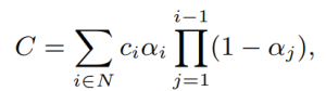
Significance score calculation aims to find Gaussians that have no impact or little overall impact. We adopt a strategy where the impact of a Gaussian is determined by considering how often it is hit by a ray. More concretely, the so called significance score GSj is calculated with 1(G(Xj ), ri) where 1(·) is the indicator function, ri is ray i for every ray in the training set and Xj is the times Gaussian j hit ri.
where j is the Gaussian index, i is the pixel, γ(Σj ) is the Gaussian’s volume, M, H, and W represents the number of training views, image height, and width, respectively. Since it is a costly operation, we apply this pruning ksg times during training with a decay factor considering the percentile removed in the previous round.
b) Spherical Harmonic (SH) MaskingSHs are used to represent view dependent color for a Gaussian, however, one can appreciate that not all Gaussians will have the same levels of varying colors depending on the scene, which provides a further pruning opportunity. We adopt a strategy where SH bands are pruned based on a mask learned during training, and unnecessary bands are removed after the training is complete. Specifically, each Gaussian learns a mask per SH band. SH masks are calculated as in the following equation and SH values for the ith Gaussian for the corresponding SH band, l, is set to zero if its hard mask, Mshi(l), value is zero and unchanged otherwise.
![]()
where mli ∈ (0, 1), Mlsh ∈ {0, 1}. Finally, each masked view dependent color is defined as ĉi(l) = Mshi(l)ci(l) where ci(l) ∈ R(2l+1)×3. Masking loss for each degree of SH is weighted by its number of coefficients, since the number of SH coefficients vary per SH band.
c) Progressive training strategiesProgressive training of Gaussians refers to starting from a coarser, less detailed image representation and gradually changing the representation back to the original image. These strategies work as a regularization scheme.
c.1) By blurring
Gaussian blurring is used to change the level of details in an image similar. Kernel size is progressively lowered at every kb iteration based on a decay factor. This strategy helps to remove floating artifacts from the sub-optimal initialization of Gaussians and serves as a regularization to converge to a better local minima. It also significantly impacts the training time since a coarser scene representation requires less number of Gaussians to represent the scene.
c.2) By resolution
Progressive training by resolution. Another strategy to mitigate the over-fitting on training data is to start with smaller images and progressively increase the image resolution during training to help learning a broader global information. This approach specifically helps to learn finer grained details for pixels behind the foreground objects.
c.3) By scales of Gaussians
Another strategy is to focus on low-frequency details during the early stages of the training by controlling the low-pass filter in the rasterization stage. Some Gaussians might become smaller than a single pixel if each 3D Gaussian is projected into 2D, which results in artefacts. Therefore, the covariance matrix of each Gaussian is added by a small value to the diagonal element to constraint the scale of each Gaussian. We progressively change scale for each Gaussian during the optimization similar to ensure the minimum area that each Gaussian covers in the screen space. Using a larger scale in the beginning of the optimization enables Gaussians receive gradients from a wider area and therefore the coarse structure of the scene is learned efficiently.
We adopt a strategy that is more focused on the training time efficiency. We follow on separating higher SH bands from the 0th band within the rasterization, thus lower the number of updates for the higher SH bands than the diffused colors. SH bands (45 dims) cover a large proportion of these updates, where they are only used to represent view-dependent color variations. By modifying the rasterizer to split SH bands from the diffused color, we update higher SH bands every 16 iterations whereas diffused colors are updated at every iteration.
GS uses photometric and structural losses for optimization where structural loss calculation is costly. SSIM loss calculation with optimized CUDA kernels. SSIM is configured to use 11×11 Gaussian kernel convolutions by standard, where as an optimized version is obtained by replacing the larger 2D kernel with two smaller 1D Gaussian kernels. Applying less number of updates for higher SH bands and optimizing the SSIM loss calculation have a negligible impact on the accuracy, while it significantly helps to speed-up the training time as shown by our experiments.
Experimental ResultsWe follow the setup on real-world scenes. 15 scenes from bounded and unbounded indoor/outdoor scenarios; nine from Mip-NeRF 360, two (truck and train) from Tanks&Temples and two (DrJohnson and Playroom) from Deep Blending datasets are used. SfM points and camera poses are used as provided by the authors [1] and every 8th image in each dataset is used for testing. Models are trained for 30K iterations and PSNR, SSIM and LPIPS are used for evaluation. We save the Gaussian parameters in 16-bit precision to save extra disk space as we do not observe any accuracy drop compared to 32-bit precision.
Performance EvaluationOur most efficient model Trick-GS-small improves over the vanilla 3DGS by compressing the model size drastically, 23×, improving the training time and FPS by 1.7× and 2×, respectively on three datasets. However, this results in slight loss of accuracy, and therefore we use late densification and progressive scale-based training with our most accurate model Trick-GS, which is still more efficient than others while not sacrificing on the accuracy.

Table 1. Quantitative evaluation on MipNeRF 360 and Tanks&Temples datasets. Results with marked ’∗’ method names are taken from the corresponding papers. Results between the double horizontal lines are from retraining the models on our system. We color the results with 1st, 2nd and 3rd rankings in the order of solid to transparent colored cells for each column. Trick-GS can reconstruct scenes with much lower training time and disk space requirements while not sacrificing on the accuracy.
Trick-GS improves PSNR by 0.2dB on average while losing 50% on the storage space and 15% on the training time compared to Trick-GS-small. The reduction on the efficiency with Trick-GS is because of the use of progressive scale-based training and late densification that compensates for the loss from pruning of false positive Gaussians. We tested an existing post-processing step, which helps to further reduce model size as low as 6MB and 12MB respectively for Trick-GS-small and Trick-GS over MipNeRF 360 dataset. The post-processing does not heavily impact the training time but the accuracy drop on PSNR metric is 0.33dB which is undesirable for our method. Thanks to our trick choices, Trick-GS learns models as low as 10MB for some outdoor scenes while keeping the training time around 10mins for most scenes.
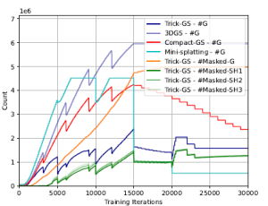
Figure 1. Number of Gaussians (#G) during training (on MipNeRF 360 – bicycle scene) for all methods, number of masked Gaussians (#Masked-G) and number of Gaussians with a masked SH band for our method. Our method performs a balanced reconstruction in terms of training efficiency by not letting the number of Gaussians increase drastically as other methods during training, which is a desirable property for end devices with low memory.
Learning to mask SH bands helps our approach to lower the storage space requirements. Trick-GS lowers the storage requirements for each scene over three datasets even though it might result in more Gaussians than Mini-Splatting for some scenes. Our method improves some accuracy metrics over 3DGS while the accuracy changes are negligible. Advantage of our method is the requirement of 23× less storage and 1.7× less training time compared to 3DGS. Our approach achieves this performance without increasing the maximum number of Gaussians as high as the compared methods. Fig. 1 shows the change in number of Gaussians during training and an analysis on the number of pruned Gaussians based on the learned masks. Trick-GS achieves comparable accuracy level while using 4.5× less Gaussians compared to Mini-Splatting and 2× less Gaussians compared to Compact-GS, which is important for the maximum GPU consumption on end devices. Fig. 2 shows the qualitative impact of our progressive training strategies. Trick-GS obtains structurally more consistent reconstructions of tree branches thanks to the progressive training.
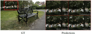
Figure 2. Impact of progressive training strategies on challenging background reconstructions. We empirically found that progressive training strategies as downsampling, adding Gaussian noise and changing the scale of learned Gaussians have a significant impact on the background objects with holes such as tree branches.
Ablation StudyWe evaluate the contribution of tricks in Tab. 2 on MipNeRF360 – bicycle scene. Our tricks mutually benefits from each other to enable on-device learning. While Gaussian blurring helps to prune almost half of the Gaussians compared to 3DGS with a negligible accuracy loss, downsampling the image resolution helps to focus on the details by the progressive training and hence their mixture model lowers the training time and the Gaussian count by half. Significance score based pruning strategy improves the storage space the most among other tricks while masking Gaussians strategy results in lower number of Gaussians at its peak and at the end of learning. Enabling progressive Gaussian scale based training also helps to improve the accuracy thanks to having higher number of Gaussians with the introduced split strategy.
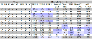
Table 2. Ablation study on tricks adopted by our approach using‘bicycle’ scene. Our tricks are abbreviated as BL: progressive Gaussian blurring, DS: progressive downsampling, SG: significance pruning, GM: Gaussian masking, SHM: SH masking, AT: accelerated training, DE: late densification, SC: progressive scaling. Our full model Trick-GS uses all the tricks while Trick-GS-small uses all but DE and SC.
Summary and Future DirectionsWe have proposed a mixture of strategies adopted from the literature to obtain compact 3DGS representations. We have carefully designed and chosen strategies from the literature and showed competitive experimental results. Our approach reduces the training time for 3DGS by 1.7×, the storage requirement by 23×, increases the FPS by 2× while keeping the quality competitive with the baselines. The advantage of our method is being easily tunable w.r.t. the application/device needs and it further can be improved with a post-processing stage from the literature e.g. codebook learning, huffman encoding. We believe a dynamic and compact learning system is needed based on device requirements and therefore leave automatizing such systems for future work.
The post A Balanced Bag of Tricks for Efficient Gaussian Splatting appeared first on ELE Times.
In the 50s, George Philbrick introduced and commercialized the first op-amp (as a potted module, not an IC). Here is a page from his application notes.
. Here is a page from his application notes.") | submitted by /u/1Davide [link] [comments] |
Basic design considerations for anti-tampering circuits

Tamper detection devices, commonly built around switches and sensors, employ several techniques according to design specifications and operating environments. T. K. Hareendran examines several anti-tampering device designs to educate and inform users on various aspects of tamper detection circuits. He also presents anti-tampering use cases built around switches and sensors.
Read the full article at EDN’s sister publication, Planet Analog.
Related Content
- Prevent tampering in energy meters
- Achieve tamper-proof capacitive sensing
- What tamper detection IP brings to SoC designs
- Don’t trust your tamper detection circuitry, it may be dumb?
- Anti tamper real time clock (RTC) – make your embedded system secure
The post Basic design considerations for anti-tampering circuits appeared first on EDN.
How find track
 | Inverter pcb [link] [comments] |
Моніторинг харчових відходів у КПІ ім. Ігоря Сікорського

У відповідності до вимог законодавства України, зокрема законів України «Про якість та безпеку харчових продуктів і продовольчої сировини», «Про управління відходами», «Про охорону навколишнього природного середовища», «Про захист прав споживачів», «Про забезпечення санітарного та епідемічного бл
Synopsys Interconnect IPs Enabling Scalable Compute Clusters
Courtesy: Synopsys
Recent advancements in machine learning have resulted in improvements in artificial intelligence (AI), including image recognition, autonomous driving, and generative AI. These advances are primarily due to the ability to train large models on increasingly complex datasets, enabling better learning and generalization as well as the creation of larger models. As datasets and model sizes grow, there is a requirement for more powerful and optimized computing clusters to support the next generation of AI.
With more than 25 years of experience in delivering field-proven silicon IP solutions, we are thrilled to partner with NVIDIA and the NVIDIA NVLink ecosystem to enable and accelerate the creation of custom AI silicon. This strategic collaboration will leverage Synopsys’ expertise in silicon IPs to assist in the development of bespoke AI silicon, forming the foundation for advanced compute clusters aimed at delivering the next generation of transformative AI experiences.
Compute challenges with larger datasets and increasingly large AI modelsTraining trillion-parameter-plus models on large datasets necessitates substantial computational resources, including specialized accelerators such as Graphics Processing Units (GPUs) and Tensor Processing Units (TPUs). AI computing clusters incorporate three essential functions:
- Compute — implemented using processors and dedicated accelerators.
- Memory — implemented as High Bandwidth Memory (HBM) or Double Data Rate (DDR) with virtual memory across the cluster for memory semantics.
- Storage — implemented as Solid State Drives (SSDs) that efficiently transfer data from storage to processors and accelerators via Peripheral Component Interconnect Express (PCIe)-based Network Interface Cards (NICs).
Retimers and switches constitute the fabric that connects accelerators and processors. To enhance the computational capabilities of the cluster, it is necessary to increase capacity and bandwidth across all functions and interconnects.
Developing increasingly sophisticated, multi-trillion-parameter models requires the entire cluster to be connected over a scale-up and scale-out network so it can function as a unified computer.

Figure 1: A representative compute cluster with scale-up and scale-out network.
Standards-based IPs for truly interoperable compute clustersThe successful deployment of next-generation computing clusters relies on silicon-verified interconnects that utilize advanced process node technology and guarantee interoperability. Standardized interconnects enable an interoperable, multi-vendor implementation of a cluster.
PCIe is an established standard for processor-to-accelerator interfaces, ensuring interoperability among processors, NICs, retimers, and switches. Since 1992, the PCI-SIG has been defining Peripheral Component Interconnect (PCI) solutions, with PCIe now in its seventh generation. The extensive history and widespread deployment of PCIe ensure that IP solutions benefit from the silicon learning of previous generations. Furthermore, the entire ecosystem developing processors, retimers, switches, NICs, and SSDs possesses significant deployment experience with PCIe technology. Our complete IP solution for PCIe 7.0 is built upon our experience with more than 3,000 PCIe designs, launched in June 2024 with endorsements from ecosystem partners such as Intel, Rivos, Xconn, Microchip, Enfabrica, and Kandou.
When deploying trained models in the cloud, hyperscalers aim to continue utilizing their software on custom processors that interface with various types of accelerators. For NVIDIA AI factories, NVLink Fusion provides another method for connecting processors to GPUs.
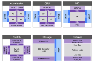
Figure 2: Components and interconnects of a next-generation compute cluster.
Accelerators can be connected in various configurations, affecting the efficiency of compute clusters. Scale-up requires memory semantics for a virtual memory pool across the cluster, while scale-out involves connecting tens-of-thousands to hundreds-of-thousands of GPUs with layers of switching and congestion management. Unlike scale-up, scale-out is more latency-tolerant and designed for bandwidth oversubscription to suit AI model data parallelism. In December 2024, we launched our Ultra Accelerator Link (UALink) and Ultra Ethernet solution to connect accelerators efficiently. The solution, which was publicly supported with quotes from AMD, Juniper and Tenstorrent, is based on silicon-proven 224G PHY and more than 2,000 Ethernet designs.
Trillion-parameter models demand extensive memory storage and high data rates for low latency access, necessitating increased memory bandwidth and total capacity. HBM provides both substantial capacity and high bandwidth. Our HBM4 IP represents the sixth generation of HBM technology, offering pin bandwidths up to 12 Gbps, which results in an overall interface bandwidth exceeding 3 TBps.
Co-packaged multi-die aggregation not only enhances compute throughput by overcoming the limitations of advanced fabrication processes but also facilitates the integration of optical interconnects through emerging Co-Packaged Optical (CPO) technologies. Since 2022, we have been developing linear electro-optical (EO) interfaces to create energy-efficient EO links. The Universal Chiplet Interconnect Express (UCIe) standard has provided a well-defined path for multi-vendor interoperability. In collaboration with Intel in 2023, we successfully demonstrated the first UCIe-connected, chiplet-based test chip.
Multi-die integration poses challenges for heat dissipation, potentially impacting temperature-sensitive photonic components or causing thermal runaway. Our comprehensive multi-die solution, including Die-to-Die IP, HBM IP, and 3DIC Compiler for system-in-package integration, provides a reliable and robust multi-die implementation.
Adopting well-established and extensively validated IP solutions across critical interconnects – from processor-accelerator interfaces to advanced multi-die architectures and HBM – mitigates the risks associated with custom design and integration. Pre-verified IPs streamline the design and verification process, accelerate timelines, and ultimately pave the way for successful first-pass silicon, enabling the rapid deployment of innovative and interoperable compute clusters.
The post Synopsys Interconnect IPs Enabling Scalable Compute Clusters appeared first on ELE Times.
Redefining Robotics: High-Precision Autonomous Mobile Robots
Courtesy: Lattice Semiconductors
Imagine a robot navigating a crowded factory floor, rerouting itself in real-time around equipment, humans, and unexpected obstacles — all while maintaining motion control and system stability. This isn’t a distant vision; this is the reality engineered by Agiliad in partnership with Lattice Semiconductor.
In a market full of autonomous mobile robots (AMRs) that rely on generic control stacks and prebuilt kits, this AMR stands out as a deep-tech system, purpose-built for intelligent indoor mobility. Unlike conventional AMRs that often trade performance for modularity or ease of deployment, this robot integrates a custom motion control framework based on Lattice’s Certus-NX FPGA, along with a ROS2-based advanced SLAM (Simultaneous Localization and Mapping), sensor fusion, and navigation stack running on NVIDIA Jetson Orin— all tightly orchestrated for low-latency, high-reliability operation.
This next-generation AMR is more than just mobile — it’s aware, adaptable, and engineered for deterministic control in real-world conditions. Designed for use in industrial settings, research labs, and beyond, the robot brings together embedded intelligence, energy efficiency, and full-stack integration to set a new benchmark for autonomous systems.
Key Features of the Robot: The Intelligence Behind the Robot
Advanced Localization & Mapping: RTAB-Map SLAM, a robust loop-closure-enabled algorithm, leverages both 3D lidar and camera feeds for consistent mapping even in environments with visual and spatial ambiguities.
- 3D Obstacle Detection & Avoidance: Using a combination of 3D voxel layers and spatio-temporal layers, the robot dynamically detects and navigates around static and moving objects — maintaining safe clearance while recalculating routes on the fly.
- Path Planning: The navigation stack uses the SMAC (Search-Based Motion Planning) planner for global routing and MPPI (Model Predictive Path Integral) for locally optimized trajectories, allowing real-time adaptation to dynamic environmental changes.
- Precision Motion Control via FPGA: BLDC motors are governed by Lattice Certus-NX FPGAs executing custom PI (proportional integral) control loops in hardware, ensuring smooth acceleration, braking, and turning — critical for safety in confined spaces.
Sensor Fusion for Environmental Awareness :
Lidar and stereo camera data is processed on the Lattice Avant-E FPGA and fused with point cloud information to detect and differentiate humans and objects, providing real-time environmental awareness for safe and adaptive navigation.

System Architecture Breakdown Diagram
The AMR’s architecture is a layered, modular system built for reliability, scalability, and low power consumption. Jetson handles ROS2 algorithms, while the Lattice FPGAs manage motion control.
- Robot Geometry and Integration with ROS2 : The robot’s geometry and joints are defined in a URDF model derived from mechanical CAD files. The Robot State Publisher node in ROS2 uses this URDF to publish robot structure and transform data across the ROS2 network.
- Lattice Avant-E FPGA Based Sensor Fusion : Sensor data from lidar and stereo vision cameras is transmitted to the Avant-E FPGA over UDP. Avant-E employs OpenCV for real-time image identification and classification, fusing visual data with point cloud information to accurately detect and differentiate humans from other objects in the environment. This fused data — including human-specific classification and distance metrics — is then transmitted to the ROS2 framework running on NVIDIA Jetson. This high-fidelity sensor fusion layer ensures enhanced situational awareness, enabling the robot to make informed navigation decisions in complex, dynamic settings.
- SLAM & Localization: Lidar provides a 3D point cloud of the environment, while the camera supplies raw image data. An RTAB-Map (Real-Time Appearance-Based Mapping) processes this information to create a 3D occupancy grid. Odometry is derived using an iterative closest point (ICP) algorithm, with loop closure performed using image data. This enables continuous optimization of the robot’s position, even in repetitive or cluttered spaces.
- Navigation: Navigation generates cost maps by inflating areas around obstacles. These cost gradients guide planners to generate low-risk paths. SMAC provides long-range planning, while MPPI evaluates multiple trajectory options and selects the safest path.
- ROS2 Control and Differential Drive Kinematics: ROS2 computes a command velocity (linear and angular) which is translated into individual wheel velocities using differential drive kinematics.
- Hardware Interface: This layer ensures integration between ROS2 and the robot’s hardware. Serial communication (UART) between Jetson and Certus-NX transmits motor velocity commands in real-time.
- Lattice Certus-NX FPGA-Based Motion Control: Lattice’s Certus-NX FPGA executes real-time motor control algorithms with high reliability and minimal latency, enabling deterministic performance, efficient power use, and improved safety under industrial loads:
PI Control Loops for velocity and torque regulation, using encoder feedback to ensure performance regardless of frictional surface conditions.
Commutation Sequencer that uses hall sensor feedback to control 3-phase BLDC motor excitation.
How It All Works Together: A Decision-Making Snapshot

The robot’s intelligence simulates a real-time decision-making loop:
Where am I?
The robot localizes using RTAB-Map SLAM with loop closure, updating its position based on visual and spatial cues.
Where should I go?
A user-defined goal (set via touchscreen or remote interface) is passed to the global planner, which calculates a safe, efficient route using SMAC.
How do I get there?
The MPPI planner simulates and evaluates dozens of trajectories in real-time, using critic-based scoring to dynamically adapt to the robot’s surroundings.
What if something blocks the path?
Sensor data updates the obstacle map, triggering real-time replanning. If no safe path is found, recovery behaviors are activated via behavior servers.
| Component / Design Element | Rationale |
| Differential Drive | Simpler control logic and reduced energy usage compared to omni-wheels |
| Lidar Placement (Center) | Avoids blind spots; improves loop closure and mapping accuracy |
| Maxon BLDC Motors | High torque (>4.5 Nm) for payload handling and smooth mobility |
| Certus-NX FPGA Motion Control | Enables deterministic control with low CPU overhead |
| Camera Integration | Improves visual SLAM and scene understanding |
| Convex Caster Wheels | Reduces ground friction, enhances turning in confined areas |
| Cooling Architecture | Fans and vents maintain safe operating temperatures |
| Jetson as CPU | Provides headroom for future GPU-based algorithm integration |
Lattice FPGA Technology
Lattice’s Certus-NX and Avant-E FPGAs deliver complementary capabilities that are critical for autonomous robotic systems:
- Low Power Consumption : Extends battery life in mobile systems
- Real-Time Performance: Delivers responsive control loops and fast data handling
- Flexible Architecture : Supports custom control logic and sensor interfaces
Combined with NVIDIA Jetson Orin and embedded vision tools, the result is a scalable and adaptable robotic platform.
Looking Ahead: Enabling the Future of Robotics
Agiliad’s engineering model emphasizes deep system-level thinking, rapid prototyping, and cross-domain integration, delivering a fully operational system within a compressed development timeline by leveraging low power Lattice FPGAs. This reflects Agiliad’s deep expertise in full-stack design and multidisciplinary integration across mechanical, electrical, embedded, and software.
The post Redefining Robotics: High-Precision Autonomous Mobile Robots appeared first on ELE Times.
The 2025 Google I/O conference: A deft AI pivot sustains the company’s relevance

The fundamental difference between Microsoft and Google’s dueling mid-May keynotes this year comes down sizzle versus steak. And that isn’t just my opinion; I can even quantify the disparity that others apparently also ascertained. As noted in my recent coverage of Microsoft’s 2025 Build conference, the full keynote ran for a minute (and a few seconds) shy of 2 hours:
But The Verge was able to condense the essentials down to a 15-minutes (and a few seconds) summary video, 1/8th the length of the original:
What about Google’s day-later alternative? It was only a couple of minutes shorter in total:
But this time, The Verge was only able to shrink it down to around 1/3 the original length, resulting in a 32-minute (and change) summary video:
Translation: nearly the same keynote duration, but much more “meat” in the Google keynote case. And that’s not even counting the 70-minute developer-tailored keynote that followed it:
That said, in fairness, I’ll point out that Google’s own summary video for the keynote was only 10 minutes long, so…
What did Google’s presenters cover in those 3+ two-keynote hours, and more generally across the two-day event (and its virtual-event precursor)? Glad you asked. In the sections that follow, I’ll touch on what I thought were at least some of the high points. For more, check out Google’s summary blogs for the developer community and the public at large, along with the conference coverage summary pages from folks like 9to5Google, Engadget, The Verge and Wired.

Conceptually similar to what Microsoft had done, Google decided to release some of its news ahead of the main event. This time, though, it was one week prior, not two. And the focus this time was on software, not hardware. Specifically, Google discussed its upcoming Expressive Design revamp of the core Android UI and associated apps, along with planned added-and-enhanced features for the O/S and apps, and related evolutions of the Android variants tailored for smart watches (Wear OS), smart glasses and headsets (Android XR), vehicles (Android Auto), displays (Google TV), and any other O/S “spins” I might have overlooked at the moment. In the process, Google got the jump on Apple, who will reportedly announce a conceptually similar revamp for its various O/Ss in a couple of weeks (stay tuned for my coverage)!
I’ll talk more about Android XR and its associated hardware, as Google did at I/O itself, in a separate topic-focused section to come later in this piece.
Multimodal large language modelsGemini, as I’ve discussed in past years’ Google I/O reports and other writeups, is the company’s suite of proprietary deep learning models, all becoming increasingly multimodal in their supported data input-and-output diversity. There are currently three primary variants:
- Pro: For coding and complex prompts
- Flash: For fast performance on complex tasks, and
- Flash-lite: For cost-efficient performance
Plus, there’s Gemma, a related set of models, this time open source, which, thanks to their comparatively low resource demands, are also useful for on-device inference with edge systems.
Latest v2.5 of Gemini Pro and Gemini Flash had both already been unveiled, but at I/O Google touted iterative updates to both of them, improving responsiveness, accuracy and other metrics. Also unveiled, this time first-time, was Gemma 3n, specifically tailored for mobile devices. And also newly announced was Gemini Live, which supports the real-time analysis and interpretation of (and response to) live audio and video feeds coming from a camera and microphone. If you’re thinking this sounds a lot like Project Astra, which I mentioned at the tail-end of last year’s Google I/O coverage (albeit not by name)…well, you’d be spot-on.
AI integration into other Google products and services…including searchJust as Microsoft is doing with its operating system and applications, Google is not only developing user direct-access capabilities to Gemini and Gemma via dedicated apps and web interfaces, it’s also embedding this core AI intelligence into its other products, such as Gmail, various Workspace apps, and Google Drive.
The most essential augmentation, of course, is that of the Google Search engine. It was Google’s first product and remains a dominant source of revenue and profit for it and parent company Alphabet, by virtue of the various forms of paid advertising it associates with search results. You may have already noticed the “AI Overview” section that for a while now has appeared at the top of search results pages, containing a summary explanation of the searched-for topic along with links to the pages used to generate that explanation:
 Well, now (as I was writing this piece, in fact!) “AI Mode” has its own tab on the results page:

And similarly, there’s now an “AI Mode” button on the Google Search home page:

Google is even testing whether to relocate that button to a position where it would completely replace the longstanding “I’m Feeling Lucky” button.
It wasn’t too long ago when various tech pundits (present company excluded, to be clear) were confidently forecasting the demise of Google’s search business at the hands of upstarts like OpenAI (more on them later). But the company’s “deft pivot” to AI teased in the title of this piece has ensured otherwise (at least until regulatory entities may say otherwise)…perhaps too much, it turns out. As I’ve increasingly used AI Overview (now AI Mode), I find that its search results summaries are often sufficient to answer my question without compelling me to click through to a content-source page, a non-action (versus tradition) that suppresses traffic to that page. Google has always “scraped” websites to assemble and prioritize search results for a given keyword or phrase, but by presenting the pages’ information itself, the company is now drawing the ire of publishers who are accusing it of content theft.
Rich content generationTake generative AI beyond LLMs (large language models) with their rudimentary input and output options (at least nowadays, seemingly…just a couple of years ago, I was more sanguine about them!), and you’re now in the realm of generating realistic still images, videos, audio (including synthesized music) and the like. This is the realm of Google’s Imagen (already at v4), Veo (now v3), and Lyria (v2 and new RealTime) models and associated products. Veo 3, for example, kicked off the 2025 Google I/O via this impressive albeit fanciful clip:
Here’s another (less silly overall therefore, I’d argue, even more impressive) one from Google:
More synthesized video examples and their associated text prompts can be found at the Veo page on the Google DeepMind site. Veo 3 is already in public release, with oft-impressive albeit sometimes disturbing results and even real-life mimickers. And combine audio, video and still images, add some additional scripting smarts, and you’ve got the new AI filmmaking tool Flow:
Who would have thought, just a few short years ago, that the next Spielberg, Scorsese, Hitchcock, Kubrick, Coppola or [insert your favorite director here] would solely leverage a keyboard and an inference processor cloud cluster as his or her content-creation toolbox? We may not be there yet, but we’re getting close…
Coding assistantsCoding is creative, too…right, programmers? Jules is Google’s new asynchronous coding agent, unveiled in Google Labs last December and now in public beta, where it goes up against
OpenAI’s recently delivered one-two punch of the internally developed Codex and acquisition (for $3B!) of Windsurf. That said, as VentureBeat also notes, it’s not even the only AI-powered coding tool in Google’s own arsenal: “Google offers Code Assist, AI Studio, Jules and Firebase”.
Android XR-based products (and partnerships)Google co-founder Sergey Brin made a curious onstage confession during a “fireside chat” session at Google I/O, admitting that he “made a lot of mistakes with Google Glass”:

His critique of himself and the company he led was predominantly two-fold in nature:
- Google tried to “go it alone” from a hardware development, manufacturing and marketing standpoint, versus partnering with an established glasses supplier such as Italian eyewear company Luxottica, with whom Meta has co-developed two generations (to date) of smart glasses (as you’ll soon learn about in more detail via an upcoming sorta-teardown by yours truly), and
- The bulbous liquid crystal on silicon (LCoS) display in front of one of the wearer’s eyes ensured that nobody would mistake them for a conventional pair of glasses…a differentiation which was not advantageous for Google.

Judging from the 2025 Google I/O messaging, the company seems determined not to make the same mistake again. It’s partnering with Warby Parker, Korea-based Gentle Monster, Samsung and Xreal (and presumably others in the future) on smart glasses based on its Android XR platform…glasses that it hopes folks will actually want to be seen wearing in public. Samsung is also Google’s lead partner for a VR headset based on Android XR…the “extended reality” (XR) that Google envisions for the operating system spans both smart glasses—with and without integrated augmented reality displays—and head-mounted displays. And it not only did live demos during the keynote but also gave attendees the chance to (briefly) try out its prototype smart glasses, glimpsed a year ago in the Project Astra clip I mentioned earlier, for themselves.
Google BeamTwo years ago, I noted that the way-cool Project Starline hologram-based virtual conferencing booth system announced two years earlier (during COVID-19 lockdowns; how apropos):
had subsequently been significantly slimmed down and otherwise simplified:
Fast forward two more years to the present and Google has rebranded the 3D-rendering technology as Beam, in preparation for its productization by partners such as HP and Zoom:
And in the process, Google has notably added near real-time, AI-powered bidirectional language translation to the mix (as well as to its baseline Google Meet videoconferencing service, which previously relied on captions), preserving each speaker’s tone and speaking style in the process:
Now there’s a practical application for AI that I can enthusiastically get behind!
OpenAI’s predictable (counter)punchIn closing, one final mention of one of Google’s primary competitors. Last year, OpenAI attempted to proactively upstage Google by announcing ChatGPT’s advanced voice mode one day ahead of Google I/O. This time, OpenAI attempted to suck the wind out of Google’s sails retroactively, by trumpeting that it was buying (for $6.5B!) the “io” hardware division of Jony Ive’s design studio, LoveFrom, one day after Google I/O. Not to mention the $3M allegedly spent on the “odd” (I‘m being charitable here) video that accompanied the announcement:
While I don’t at all discount OpenAI’s future prospects (or Meta’s, for that matter, or anyone else’s), I also don’t discount Google’s inherent advantage in developing personalized AI: it’s guided by the reality that it already knows (for better and/or worse) a lot about a lot of us.
How do you think this’ll all play out in the future? And what did you think about all the news and enhanced technologies and products that Google recently unveiled? Let me (and your fellow readers) know in the comments!
—Brian Dipert is the Editor-in-Chief of the Edge AI and Vision Alliance, and a Senior Analyst at BDTI and Editor-in-Chief of InsideDSP, the company’s online newsletter.
Related Content
- The 2024 Google I/O: It’s (pretty much) all about AI progress, if you didn’t already guess
- The 2023 Google I/O: It’s all about AI, don’t cha know
- Smart glasses skepticism: A look at their past, present, and future(?)
- Google’s fall…err…summer launch: One-upping Apple with a sizeable product tranche
The post The 2025 Google I/O conference: A deft AI pivot sustains the company’s relevance appeared first on EDN.
Made-in-India Chips Coming in 2025, Says Ashwini Vaishnaw
India is going to make their very first indigenous chip by the end of 2025, making a very important step towards technological advancements for this nation. Announcing this, Union Minister of Electronics and IT, Ashwini Vaishnaw, said that the chip employing 28-90nm technology is slated for rollout this year. This is envisaged as part of a larger plan for India to promote semiconductor manufacturing in the country and cut down on import dependency.
The first chip would be manufactured at Tata Electronics’ unit at Jagiroad in Assam, with an investment of 27,000 crore. The facility, coming up under the aegis of the India Semiconductor Mission, is a huge investment into the northeast and shall create many job opportunities. The government has also approved setting up the sixth fab in Uttar Pradesh through a JV of HCL and Foxconn, further deepening the semiconductor ecosystem in the country.
Minister Vaishnaw stated that the 28-90nm chips are used in various sectors such as automotive, telecommunications, power and railways. India, therefore, intends to focus on this segment that accounts for roughly 60 percent of the global semiconductor market so that it can position itself as a major market player.
Apart from manufacturing, the government is putting a greater emphasis on developing indigenous IP and design skills. Work is progressing towards the development of 25 chips with indigenous IP-aimed at improving cyber security. 13 projects are being pursued under the aegis of the Centre for Development of Advanced Computing (C-DAC), Bengaluru, thereby giving concrete expression to self-reliance and innovation.
Building an indigenous fab aligns with the objectives laid down in India’s “Digital India” concept, which works towards prompting India as a global nucleus for electronics manufacturing. India’s entry into the semiconductor industry is anticipated to have a significant impact on the economy both domestically and globally, given the continuous disruptions in the supply chain and in the rapidly evolving technological landscape.
Conclusion:
This initiative is directly in keeping with the “Digital India” vision to transform the country into a gobal hub for electronics manufacturing. With supply chain issues and technological shifts currently gripping the world, practically entering semiconductor production would certainly having far-reaching implications for the Indian economy as well as on the global level.
The post Made-in-India Chips Coming in 2025, Says Ashwini Vaishnaw appeared first on ELE Times.
Sumitomo Electric and Osaka Metropolitan fabricate GaN HEMT on 2-inch polycrystalline diamond
🎥 КПІшники — переможці масштабного хакатону MHP TECH Hackathon!

🏆 Команда Навчально-наукового механіко-машинобудівного інституту (НН ММІ) виборола перше місце зі 123 команд з усієї України у другому очному етапі масштабного хакатону від МХП, що проходив на території переробного комплексу в м. Ладижин (Вінницька область).
India will become the world’s electronics factory : We have the policy, the talent, and now the infrastructure to make it happen
India is making significant efforts to boost its electronics manufacturing industry with the goal of establishing itself as a prominent player in the global market. The electronics industry is witnessing remarkable growth and advancement, with a special emphasis on expanding manufacturing operations in India, particularly in the realm of semiconductor chips and electronics components. Noteworthy developments include the production of India’s first locally developed semiconductor chip in Gujarat, the initiation of state-level electronics component manufacturing programs in Tamil Nadu, and the implementation
of various PLI (Production Linked Incentive) schemes aimed at promoting local production. Furthermore, efforts are underway to establish a repairability index for electronics to tackle e-waste, and the government is actively promoting research and development as well as innovation within the sector.
India is currently enacting a series of strategic measures to enhance its electronics manufacturing sector with the aim of positioning itself as a key player on the global stage in the field of electronics production.
The “Make in India” initiative, launched to transform India into a global manufacturing hub, focuses on enhancing industrial capabilities, fostering innovation, and creating world-class infrastructure. This initiative aims to position India as a key player in the global economy by attracting investments, promoting skill development, and encouraging domestic manufacturing.
The Phased Manufacturing Programme (PMP) was introduced by the government to boost the domestic value addition in the manufacturing of mobile phones as well as their sub-assemblies and parts. The primary objective of this scheme is to stimulate high-volume production and establish a robust local manufacturing framework for mobile devices.
To enhance the growth of domestic manufacturing and foster investment in the mobile phone value chain, including electronic components and semiconductor packaging, the government introduced the Production Linked Incentive Scheme (PLI) for Large Scale Electronics Manufacturing. This initiative offers incentives ranging from 3% to 6% on incremental sales of products manufactured in India within target segments such as Mobile Phones and Specified Electronic Components.
Another initiative is the PLI scheme for passive electronic components, with a budget of INR 229.19 billion. This scheme aims to promote the domestic manufacturing of passive electronic components such as resistors and capacitors. These components are integral to various industries such as telecom, consumer electronics, automotive, and medical devices.
The Semicon India Program, initiated in 2021 with a considerable budget of ₹76,000 crore, aims to bolster the domestic semiconductor sector through a mix of incentives and strategic alliances. The comprehensive initiative not only focuses on the development of fabrication facilities (fabs) but also emphasizes on enhancing packaging, display wires, Outsourced Semiconductor Assembly and Testing (OSATs), sensors, and other vital components crucial for a thriving semiconductor ecosystem.
The Indian government is promoting research and development, along with fostering innovation, within the electronics industry. India is actively engaging in collaborations with international firms, with a specific focus on high-tech manufacturing and chip design.
India’s progress in establishing itself as a prominent destination for electronic manufacturing on the global stage has been characterized by a series of deliberate policy decisions, significant advancements in infrastructure, and a growing interconnectedness with the international community. Through careful leveraging of present circumstances and the diligent resolution of pertinent obstacles, India continues to make substantial strides towards the realization of its ambitious vision.
Devendra Kumar
Editor
The post India will become the world’s electronics factory : We have the policy, the talent, and now the infrastructure to make it happen appeared first on ELE Times.
Silicon Photonics Raises New Test Challenges
Semiconductor devices continuously experience advancements leading to technology and innovation leaps, such as we see today for applications in AI high-performance computing for data centers, edge AI devices, electrical vehicles, autonomous driving, mobile phones, and others. Recent technology innovations include Angstrom-scale semiconductor processing nodes, high-bandwidth memory, advanced 2.5D/3D heterogeneous integrated packages, chiplets, and die-to-die-interconnects to name a few. In addition, silicon photonics in a co-packaged optics (CPO) form factor promises to be a key enabling technology in the field of high-speed data communications for high-performance computing applications.
What is CPO?
CPO is a packaging innovation that integrates silicon photonics chips with data center switches or GPU computing devices onto a single substrate (see Figure 1). It addresses the growing demand for interconnects with higher bandwidth and speed, low latency, lower power consumption, and improved efficiency in data transfer for AI data center applications.

Figure 1 Co-packaged Optics (Source: Broadcom)
To understand CPO we need to first understand its constituent technologies. One such critical technology for CPO is silicon photonics. Silicon photonics provides the foundational technology for integrating high-speed optical functions directly into silicon chips. CMOS foundries have developed advanced processes based on silicon semiconductor technology to enable photonic functionality on silicon wafers. CPO uses heterogeneous integrated packaging (HIP) that integrates these silicon photonics chips directly with electronic chips, such as AI accelerator chips or a switch ASIC, on a single substrate or package. Together, silicon photonics and HIP deliver CPO products. Thus, CPO is the convergence of silicon photonics, ASICs and advanced heterogeneous packaging capability supply chains.
As mentioned earlier, CPO brings high-speed, high bandwidth, low latency, low-power photonic interconnects to the computation beachfront. In addition, photonics devices are almost loss-less for large distances enabling one such AI accelerator to share workloads with another AI accelerator hundreds of meters away, while acting as one compute resource. This high-speed and long-distance interconnect CPO fabric promises to re-architect the data center, a key innovation to unlock future AI applications.
Early CPO prototypes are being developed as of 2025 which integrate photonics “engines” with the switch or GPU ASICs on a single substrate, rather than using advanced heterogeneous packages for integration. The optical “engine” in this context refers to the packaging of the silicon photonics chips with other discrete components plus the optical fiber connector; and CPO in this context refers to the assembly of several optical engines with the switch or GPU ASICs on a common substrate.
How to Shorten CPO Time to Market?
The datacom market for CPO presents an opportunity size of about two orders of magnitude higher than what silicon photonics manufacturing supply chains have been historically accustomed to handling, such as the high-mix, low-volume products and applications in telecom and biotech. To successfully achieve CPO at this higher volume, three elements need to advance:
- The silicon photonics supply chain needs to scale up capacity and achieve high yields at wafer and at the optical engine level.
- New heterogeneous integrated packaging concepts need to be proven with the OSATs and contract manufacturers for co-packaged optics.
- New, high-volume test techniques need to be developed and proven, as the current silicon photonics testing processes are highly manual and not scalable for high volume manufacturing.
CPO technology is not mature or at high volume yet, but test equipment providers and device suppliers need to be ready for its arrival as it has a direct impact on automated test equipment test requirements, whether at the wafer, package, or system level. Investments in photonics testing capabilities are critical for developing hybrid testing systems that can keep pace with rapid advancements in photonics, and can handle both electrical and optical signals simultaneously. CPO testing requires active thermal management, high power, large package handling, custom photonic handling and alignment, high-speed digital signaling, wide-band photonic signaling, and high frequency RF signal testing.
Additionally, there are multiple test insertions from wafer to final package test that need to be optimized for test coverage, test time, and cost (see Figure 2). Expertise and experience are required to optimize the test coverage at each insertion to avoid incurring significant product manufacturing cost in both operational expense and capital equipment.

Figure 2: Silicon Photonics Wafer-to-CPO Test Insertions
CPO Test Challenges
Testing CPO devices presents unique challenges due to the diverse processes and materials involved, both electrical and photonics. A unique challenge lies in the inherent complexity of aligning optical components with the precision needed to ensure reliable test results. Optical signals are highly sensitive to minute deviations in alignment, unlike traditional electrical signals, where connection tolerances are more forgiving. The intricacies of CPO, which integrate photonics with high-digital content computing devices, demand precise positioning of lasers, waveguides, and photodetectors. Even the smallest misalignment can result in signal degradation, power loss, or inaccurate measurements, complicating test processes. As this technology advances, automated test equipment needs to evolve to accommodate the precise requirements posed by photonics and optical-electrical integration.
In addition to the precision required, the materials and processes involved in CPO introduce variability. When multiple optical chiplets from different suppliers, each using possibly different materials or designs, are packaged into a single substrate, maintaining alignment across these disparate elements becomes exponentially more difficult. Each optical chiplet may have its own unique optical properties, meaning that test equipment must handle a range of optical alignments without compromising the accuracy of signal transmission or reception. This increases the demand for automated test equipment to adapt and provide consistently reliable measurements across various types of materials and optical designs.
The time-consuming nature of achieving precise alignment also creates a significant bottleneck in high-volume semiconductor testing environments. Aligning optical components, often manually or through semi-automated processes, adds time to test cycles, which can negatively impact throughput and efficiency in production environments. To mitigate these delays, automated test equipment suppliers must invest in advanced photonics testing capabilities, such as hybrid systems that can handle both electrical and optical signals simultaneously and efficiently. These systems must also incorporate faster, more reliable alignment techniques, potentially leveraging AI-driven calibration and adaptive algorithms that can adjust in real-time.
Test meets the high-stakes needs of CPO
With the push for faster data interconnects supporting the latest industry protocols—such as PCIe 5.0/6.0/7.0 and 400G/800G/1.6T b/s Ethernet, and beyond—the stakes are high for data center reliability and performance. Any failure or suboptimal performance in data interconnects can lead to significant downtimes and performance bottlenecks. Consequently, there is a greater emphasis on enhanced test coverage to identify and address potential issues before the components are deployed in data centers. As a result, the semiconductor test industry must provide comprehensive test solutions that cover all aspects of component performance, including signal integrity, thermal behavior, and power consumption under a range of operating conditions.
Ultimately, the industry’s shift toward CPO will demand a transformation in test methodologies and equipment, with special emphasis on accurate optical alignment at all test insertions, from wafer to CPO packages. Semiconductor test leaders who invest in advanced photonics testing systems will be better positioned to handle the complexities of this emerging technology, ensuring that they can keep pace with both rapid advancements and growing market demands.
Teradyne is at the forefront of these innovations anticipating new technologies and taking a proactive approach to developing flexible and effective automated test equipment capabilities for the latest advancements in semiconductor packaging and materials.

Dr. Jeorge S. Hurtarte
Senior Director, SoC Product Strategy Semiconductor Test group
Teradyne
The post Silicon Photonics Raises New Test Challenges appeared first on ELE Times.
Pages


![[link]](https://i.redd.it/iq01yctahl4f1.jpeg)