
Feed aggregator
Anritsu Gains Certification for Latest DisplayPort 2.1 Video Interface Standard Testing Solution
Anritsu Corporation announced that its receiver test (SINK Test) solution for the latest DisplayPort 2.1 standard has been certified by the Video Electronics Standards Association (VESA), the international standards organization. Combining Anritsu’s Signal Quality Analyzer-R MP1900A with automation software from Granite River Labs (GRL) or Teledyne LeCroy achieves automated verification of data transmission quality and calibration.
DisplayPort 2.1 enables the digital transmission of high-definition and high-refresh-rate video, such as 8K. The standard is still being developed. Recently, the integration of the USB Type-C specifications has led to a significant expansion in the versatility of DisplayPort 2.1 and its adoption across a wide range of applications. However, a challenge facing the development of products that comply with the new standard is that manually verifying transmission signal quality and calibrating are time-consuming due to the complexity of the test equipment settings and the lengthy configuration and test procedures. This solution improves development efficiency and ensures the quality of video data transmission by automating the testing and calibration processes.
The post Anritsu Gains Certification for Latest DisplayPort 2.1 Video Interface Standard Testing Solution appeared first on ELE Times.
Infineon expands security controller portfolio for USB tokens with new ID Key S USB for more security and versatility
Infineon Technologies AG is expanding its offering for universal serial bus (USB) tokens, dongles, security keys, and other hardware authenticators with the introduction of the new Infineon ID Key family. The newest member, the ID Key S USB is a highly secured and versatile product designed for a wide range of USB- and USB/NFC-token devices and applications. It combines the security, performance, and reliability of the Infineon SLC38 security controller with a USB bridge controller in one single package. It is a unique system-in-package solution that enables high flexibility and simplifies complex application deployments while reducing the bill of materials and related costs. Certified to highest security levels, it supports a range of use cases, including certificate-based authentication, Fast Identity Online (FIDO) authentication with device-bound passkeys, digital signatures, encryption, access control, software protection, and cryptocurrency hardware wallets.
The increasing need for secured online transactions and the growing threat of cyber-attacks have created a surge in demand for secured and hardware-backed authentication solutions. “As the market shifts towards more secured and convenient authentication methods, we see a growing trend towards the adoption of advanced security solutions,” said Maurizio Skerlj, Senior Vice President and Product Line Head Authentication & Identity Solutions at Infineon’s Connected Secure Systems Division. “With the ID Key S USB, we are well-positioned to address this trend and provide our customers with a robust solution that meets their needs.”
The ID Key S USB offers a range of key features that support its secured and versatile design and boasts a comprehensive array of features. Its high-performance capabilities are driven by a 32-bit CPU clocked at 100 MHz and a large 24 kB RAM, enabling ultra-fast and secured execution of applications and delivering excellent operating system performance for a wide range of use cases. The device also offers sufficient memory, with non-volatile memory sizes of up to 800 kB providing ample storage for large amounts of data, cryptographic keys, software, and multiple applications. Furthermore, the ID Key S USB has achieved highest security levels, with certification to CC EAL 6+ (high) and compliance with FIPS 140-3 hardware requirements, allowing customers to apply for FIPS 140-3 certification for their product. The ID Key S USB features a compact footprint of 4 x 4 x 0.85 mm, making it ideal for integration into space-critical token devices.
The post Infineon expands security controller portfolio for USB tokens with new ID Key S USB for more security and versatility appeared first on ELE Times.
Dhruva’s Solis+ space-grade solar panels to be used by Pixxel
💛💙 Навчання ветеранів у КПІ ім. Ігоря Сікорського
Ветерани й ветеранки, усі учасники бойових дій! Запрошуємо вас приєднуватися до великої КПІшної родини!
Наразі у КПІ ім. Ігоря Сікорського вже навчаються 79 учасників бойових дій (денна форма —22, заочна форма — 57).
System-level test’s expanding role in producing complex chips

System-level test (SLT), once used largely as a stopgap measure to catch issues missed by automated test equipment (ATE), has evolved into a necessary test insertion for high-performance processors, chiplets, and other advanced computational devices. Today, SLT is critical for ensuring that chips function correctly in real-world conditions, and all major CPUs, APUs, and GPUs now go through an SLT insertion before shipment.
Adding SLT in production is being considered for network processors and automotive processors for driver assistance. However, implementing SLT techniques effectively at scale poses key challenges in terms of managing costs, test times, and manufacturers’ expectations.
One of the biggest misconceptions about SLT is that it functions like ATE. ATE primarily uses pre-defined test patterns to stimulate circuit paths and check expected responses within individual cores or circuit blocks. On the other hand, SLT focuses on system interactions that occur between those cores or outside the chip.
That includes software, power management, sensor integration, and communication between internal cores and peripheral devices. Since SLT is often used to test cutting-edge chips, the test environment needs to be flexible so that it can handle application-specific conditions and different interface protocols.
This distinction is particularly relevant as the industry shifts toward chiplet-based architectures. With chiplets, manufacturers need to test how signals propagate across multiple interconnected dies, rather than just validating individual components in isolation.
Test pattern creation for traditional ATE methods, used for chip package-level testing, offers limited access to internal interactions within a multi-chip package. SLT, on the other hand, can exercise how data flows between chiplets and how this influences performance, power consumption, and overall system functionality.
However, this approach comes with its own unique complications, especially since many SLT methodologies are implemented manually.
Test coverage challenges
Using conventional design for test (DFT) techniques to generate test patterns ahead of production ramp, chip designers are lucky to get 99% coverage of all the transistors. However, for devices with 100 billion transistors, such as today’s advanced artificial intelligence (AI) processors, 1 billion transistors still go untested. Using purely ATE test methods, achieving that last 1% of test coverage could take months of development and significant tester time.
Moreover, today’s complexity of integrating heterogeneous chiplets into one large package challenges the stability and repeatability of the electromechanical stack-up in a high-volume test environment. There are limited test access points to the outside world that must stimulate pathways through multiple dies.
Because the packages are large, there may be warpage and restricted mechanical compression points for actuating the device-under-test (DUT) connections in the socket. Exercising processors and memories inside the same package under extreme test conditions, there are inevitable hot spots that must be managed to prevent damage to the device.
To provide a durable automated system-level tester with high availability in manufacturing, the customer test content must be tightly integrated with socket actuation and thermal control, along with power management and test sequencing.
Compounding the complexity of test content development is how many parties may be involved in optimizing the SLT insertion. Vendors of SLT equipment, sockets, and design and test IP must collaborate with the silicon designer/integrator, custom ASIC end-user, outsourced semiconductor assembly and test providers (OSATs), board designers, and even customers—for example, manufacturers of data centers, computer vendors and cellphone devices—to make sure the test station represents the real-world application it’s intended to test.
As the demand for processing power increases, chip designs have evolved to meet market requirements. This increase in processing power results in higher energy consumption and heat generation. So, test time for a typical SLT insertion can be a half hour or more, requiring many test stations to meet the monthly volume demands.
The buildings built to test the parts must have special facilities for electrical power and thermal control. Therefore, these test facilities aim to maximize their investment by testing as many devices in the smallest floor space as possible. However, the devices and their test application boards are getting bigger and consume more power.
Emerging developments in chip testing
Chip designers and EDA vendors have developed and introduced new DFT techniques that allow structural test content to be delivered as packetized data over standard high-speed serial ports like USB and PCIe. During SLT, these ports must be enumerated at the application level so that the port operates as intended.
Once this connection is made, the test program can switch into a test mode using a small number of high-speed pins to run structural test patterns or other built-in self-test functions. Once these serial data ports are working, the test content can be reused and correlated either to ATE with similar test stations (such as Link Scale) or post-silicon validation test stations (such as SiConic) to improve time to market and reuse.
Managing the heat dissipation of these high-power devices under extreme workload is a ubiquitous problem being addressed at the engineering, bench, ATE and SLT test insertions, and even in data-center-wide operation. Air, liquid, and refrigerants are all utilized, with an eye on environmental sustainability. Production test handlers have the added challenge of cycling heat and mechanical engagement multiple times per day.
The use of AI and machine learning (ML) is also being applied to semiconductor testing. Sharing the test result data between different test insertions, including ATE, burn-in, and SLT, feeds into AI and ML tools to improve yield, accelerate test-program development, and optimize test times.
Looking ahead
As semiconductor manufacturing becomes more complex, SLT will continue to grow in importance. For it to be truly effective, companies must integrate it into their overall testing strategy rather than treating it as a separate, isolated step. And the next generation of system-level testers must focus on addressing the challenges cited above. Success will require collaboration across design, test, and high-volume manufacturing teams, as well as a willingness to rethink traditional approaches to validation.
In an era defined by multi-chip packages, heterogeneous integration, and ever-tightening performance demands, SLT will remain a crucial tool for ensuring that cutting-edge chips perform as expected in real-world applications.
Davette Berry is senior director of Customer Programs & Business Development at Advantest.
Related Content
- System-level verification tool rolls
- 3 tips for system-level test-driven development
- Automating C test cases for embedded system verification
- Performance-Regression Pitfalls Every Project Should Avoid
- Understanding and comparing the differences in ESD testing
The post System-level test’s expanding role in producing complex chips appeared first on EDN.
Texas Instruments India concludes fourth annual WiSH program
Texas Instruments (TI) has wrapped up the fourth edition of its month-long Women in Semiconductors and Hardware (WiSH) program. WiSH is TI’s flagship mentorship initiative aimed at inspiring and empowering second-year female engineering students across India to pursue impactful careers in core engineering, with a focus on semiconductors and hardware. Built on the previous three editions’ success, the 2025 program attracted over 1,500 registrations and more than 190 participants, reflecting a growing interest in the initiative over the years.
“The semiconductor industry is evolving rapidly, and the need for skilled talent is greater than ever,” said Santhosh Kumar, Managing Director, Texas Instruments India. “With women representing less than 20% of the people in the technical roles in the industry the WiSH program expands access, builds confidence, and fosters engineering capabilities among aspiring women engineers in India. By investing in this next generation of talent, we are helping shape a stronger semiconductor ecosystem.”
This year’s WiSH program participants gained hands-on experience through simulation projects, lab visits, technical deep dives, and networking sessions with TI leaders. The program included three weeks of virtual mentoring, culminating in an immersive, in-person week at TI’s Bengaluru campus. During this phase, students engaged directly with mentors, industry experts, and women leaders from TI.
“The WiSH program provided me the right platform to go beyond classroom learning. We had access to labs where we gained hands-on experience in simulation and circuit design,” said Poornima Kulkarni, Analog Engineer at TI India and a previous WiSH participant. “What makes it unique is the mentorship by subject matter experts to guide aspiring engineers through the course of the program.”
Texas Instruments remains committed to fostering diversity and inclusion within the technology sector. Through initiatives such as WiSH, TI helps to bridge the gender gap in STEM fields and empower the next generation of engineers to lead and innovate in the semiconductor industry.
The post Texas Instruments India concludes fourth annual WiSH program appeared first on ELE Times.
Mouser Electronics Heads South with India Technical Roadshow
Following the resounding success of the Pune and Ahmedabad sessions, Mouser Electronics, Inc., the industry’s leading New Product Introduction (NPI) distributor with the widest selection of semiconductors and electronic components, is geared-up to continue the 6th edition of its India Technical Roadshow with upcoming stops in Chennai on July 11 and Bengaluru on July 17, 2025.
The roadshow serves as a platform for design engineers, technology leaders, FAEs, OEMs, EMS professionals and ecosystem enablers to engage with emerging developments in IoT through in-depth technical sessions, live demonstrations, and valuable networking. Our technology partners – Analog Devices, Littelfuse, Molex, Phoenix Contact, Samtec, Silicon Labs, Taiyo Yuden, Bel Fuse and Würth Elektronik showcase their newest innovations and solutions to support next-generation electronic design at the India Technical Roadshow.
“We are thrilled by the energy and enthusiasm we have experienced at the India Technical Roadshow in the past years,” said Daphne Tien, Vice President of Marketing and Business Development for Mouser APAC. “India’s technology ecosystem is evolving rapidly, and this roadshow reflects our commitment to supporting that momentum. With tailored themes and practical sessions, our aim is to deliver knowledge that truly resonates with local engineers and empowers them to turn ideas into impactful innovations.”
The Chennai event, to be held at Hyatt Regency, will focus on smart manufacturing. Participants will explore strategies to future-proof factory floors using edge computing, industrial machine vision, advanced automation, and intelligent communication protocols that enhance efficiency and reliability.
India Technical Roadshow at the Taj, MG Road, Bengaluru, will bring the series to a close with a deep dive into rugged electronics. The sessions will delve into design principles for building high-resilience systems suited for harsh environments, with insights into thermal management, shock resistance, and standards-compliant design, including MIL-STD and IP-rated components.
Mouser Electronics provides comprehensive design support through its vast technical resource library on engineering topics that will shape the future. You can access exclusive technical information through our Empowering Innovation Together series, eBooks, newsletters and new product emails, and online tools to accelerate your project.
As a global authorized distributor, Mouser offers the widest selection of the newest semiconductors, electronic components and industrial automation products. Mouser’s customers can expect 100% certified, genuine products that are fully traceable from each of its manufacturer partners. To help speed customers’ designs, Mouser’s website hosts an extensive library of technical resources, including a Technical Resource Center, along with product data sheets, supplier-specific reference designs, application notes, technical design information, engineering tools and other helpful information.
Engineers can stay abreast of today’s exciting product, technology and application news through Mouser’s complimentary e-newsletter. Mouser’s email news and reference subscriptions are customizable to the unique and changing project needs of customers and subscribers. No other distributor gives engineers this much customization and control over the information they receive. Learn about emerging technologies, product trends and more by signing up at https://sub.info.mouser.com/subscriber/.
The post Mouser Electronics Heads South with India Technical Roadshow appeared first on ELE Times.
Unipress orders Taiyo Nippo Sanso MOCVD platforms
Handy automatic zero reference for Hall effect probes

Many analog sensors today are designed to operate from a single power rail but produce output signal centered around approximately half of power supply voltage, linear hall effect sensors and MEMS accelerometers are few to name. But when their output is observed by oscilloscopes or measured by multimeters, it is desirable to bring the output centered around zero volts. This allows you to observe the physical parameters they sense with greater resolution without risking saturation of the scope or multimeter.
Figure 1 shows a simple circuit utilizing a non-volatile digital potentiometer that can be handy for automatically adjusting the zero-point virtual ground terminal of the scope with the push of a button, and keeping it steady even across power cycles.

Figure 1 Autozero circuit schematic diagram that allows the user to automatically adjust the zero-point virtual ground terminal of the scope with the push of a button.
Wow the engineering world with your unique design: Design Ideas Submission Guide
The typical application for this circuit is analyzing waveforms of the currents in a power inverter with a Hall effect DC current sensor, like SS49E, and any DSO. The sensor HE1 is ratiometric, its output is centered around Vcc/2, and the voltage difference is proportional to a product of the magnetic field and Vcc. The typical bandwidth of the sensor is 200 kHz.
A floating ~6 V battery powers the probe, and the accurate Vcc required for a calibrated conversion factor of the sensor is generated by an optional micropower LDO U4. I tried to use low-power components to extend battery life.
The adjustable reference voltage is produced by digital potentiometer U1, with its wiper driving virtual ground buffer amplifier U2B. Its output is connected to the “ground” terminal of an SMA output connector for connection to a scope or multimeter, so that the sensor output observed on CON2 is centered around zero.
The auto adjustment is performed by comparator U2A, driving the “up/down” direction input of the potentiometer. It will move the wiper tap up or down on every clock of the clock generator U3, depending on the voltage difference between the sensor output and virtual ground. When the clock generator runs at ~1.5 kHz, the tap will move to the point of balance within 100 ms and will oscillate within one tap around the balance point.
The clock generator does not run continuously. The FET Q2 will release it only when SB1 is pressed momentarily, pulling the CS signal low to enable updates of the potentiometer. There is no special timer on the enable signal for simplicity. When the button is released, all signals are parked at a high level, resulting in an update of the non-volatile setting of the potentiometer.
It is desirable to eliminate any switching within the circuit to eliminate noise, especially when sensitive measurements are needed. Q2 disables the clock oscillator, and Q1 disables the comparator to achieve that when SB1 is not pressed.
The optional R1 and D1 may help observe how the circuit reaches balance—its brightness will be half of the maximum at the balance point.
The range of balance is selected by R3, R5, and R7, which set the voltage between the upper and lower end of the resistor string in a digital potentiometer. With the values shown in the schematic, it is ~0.24 V, and the wiper steps are ~2.4 mV. The user may vary these values to set the optimum range and resolution of adjustment.
The autozero circuit may compensate for small bias and temperature drift. Press SB1 whenever the steady zero output exists at the output of the sensor to operate the circuit.
Celsiuss Watt is an engineer with a major semiconductor company and has contributed several technical publications for EDN and other electronics magazines. He enjoys handy electronics projects in his spare time
Related Content
- EDN — 10.27.94 Peltier element controls itself
- Seismometer and structural vibration meter
- Building a low-cost, precision digital oscilloscope—Part 1
- Hall-effect sensors measure fields and detect position
- Current monitor uses Hall sensor
The post Handy automatic zero reference for Hall effect probes appeared first on EDN.
Наука без кордонів: участь студенток ФМФ у програмах академічної мобільності

Стратегія розвитку КПІ ім. Ігоря Сікорського передбачає підвищення рівня академічної мобільності студентів і викладачів через програми міжнародних обмінів, літні школи, стажування тощо. Це один із пріоритетних напрямів діяльності університету задля поглиблення інтернаціоналізації та інтеграції учасників освітнього процесу в міжнародний освітньо-науковий простір, підвищення якості освіти та ефективності наукових досліджень, а також забезпечення конкурентоспроможності на ринку освітніх послуг.
Power in Motion: how self-charging phones will quite literally put power in consumer’s hands
Author: STMicroelectronics
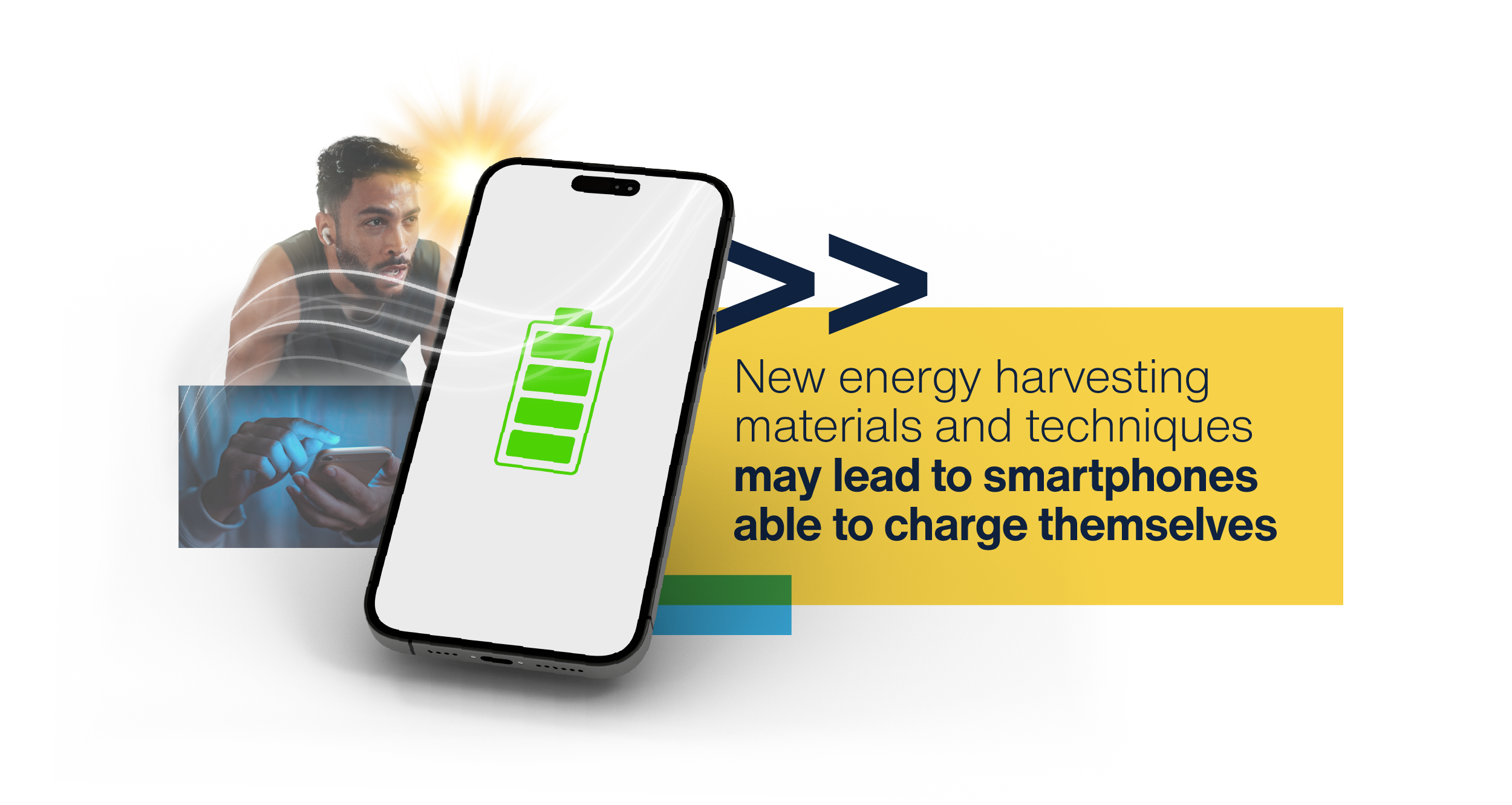
Over the past decade, smartphones have evolved far beyond their original purpose, integrating everything from complex applications to higher-quality cameras. Yet with each new capability comes the demand for more power – and with it, the need for more regular recharging. Given the need to be connected to a power socket for charging, it’s usually an act that takes the “mobile” out of mobile phone.
Several innovations are exploring solutions to this issue of ‘battery drain’. The development of more energy-efficient chips will provide the processing needed for the next generation of app and smartphone capabilities while consuming less energy. Alongside this, advances in energy management chips will more efficiently convert and distribute power within the device. And research into new energy harvesting materials and techniques may, ultimately, see smartphones able to charge themselves.
 Advancements in smartphone chip efficiency and power management
The semiconductor sector continually looks to deliver increased performance while reducing power consumption. Smartphones make use of the most advanced semiconductor process technologies. Today, this typically means sub-5nm node processes, though even smaller process nodes are in development. In simple terms, smaller nodes mean smaller transistors, which allows greater transistor density in the same area of silicon. This is key to increased performance but also supports improved energy efficiency.
Several factors support the enhanced energy efficiency and reduced power consumption of the latest generation of smartphone chips. These include shorter interconnects between transistors, lower operating voltages required by smaller transistors, transistor architectures that reduce power leakage (an issue that can increase as process node size decreases), and chips which dynamically adjust power based on device workload.
Further to the overall advancement of semiconductor process technologies, there has been an emergence of chips specifically designed for power management in devices. Power Management Integrated Circuits (PMICs) – including those from ST – control, allocate, and regulate power delivery within devices and are fundamental in optimizing performance and extending battery life. As an endorsement of the importance of power management to the smartphone sector, the PMIC for smartphones market, already valued globally at over $6 billion in 2022, is expected to grow to over $10 billion by 2030.

The PMIC within a smartphone converts power from the battery to the specific voltages needed by components like the CPU, GPU, modem, display, and memory, ensuring that each component receives stable power, crucial for performance and reliability. The PMIC also controls how power is routed to different subsystems based on usage, potentially cutting off power to unused modules – for instance GPS or Bluetooth – to save energy. The PMIC also manages battery charging itself, protecting the battery from overcharging, overheating, and over-discharging, enhancing battery life.
While improving the energy efficiency of chips and overall power management within devices will help extend battery life, research and development continues in relation to materials that may ultimately remove the need to physically recharge mobile devices entirely.
The emergence of energy harvesting materialsPiezoelectric materials, which occur both naturally or can be artificially manufactured, generate an electric charge when subject to pressure. Piezoelectric materials themselves aren’t a new discovery. Indeed, anyone who’s owned a quartz wristwatch has benefitted from their natural capabilities. But their potential in smartphones is just being unlocked.
The pressure applied to a piezoelectric material’s crystal lattice – the structure of atoms in a solid material – causes the atoms to shift slightly, creating an electric charge. This transformation of mechanical force into electricity is known as the piezoelectric effect. Natural piezoelectric materials include, as mentioned, quartz (or silicon dioxide) but also Rochelle salt, topaz and, in biological systems, bone. Many synthetic piezoelectric materials can also be manufactured.
There are several ways that the electric charge created by physical interaction with piezoelectric materials can be used by smartphones to self-charge. Users simply touching or swiping a screen, pressing device buttons, or even the movement of the smartphone itself in a bag or pocket, can result in an ongoing series of electric charges to extend battery life and reduce the regularity of charging required.
Light, heat, movement, and even air: the broader potential for energy harvestingIn addition to piezoelectric materials, research continues into how almost every natural resource could be used as an energy source for smartphones. Innovations in ultrathin, transparent photovoltaic (PV) cells integrated into smartphone screens or back panels show promising potential in the near-term. Thin film PV cells are relatively low cost, have a high level of technology readiness, and can be integrated easily within the case of a smartphone. Additional advantages are that PV cells add negligible weight to a smartphone and have the best energy per volume generation, particularly outdoors. Working in ambient light, PV cells could provide continuous “trickle charging” to mobile devices.
Similar in some ways to piezoelectric materials, triboelectric energy harvesting uses friction between materials – for instance when swiping a screen – to generate electricity. Rather than electric charge generation being a property of the material itself, triboelectric energy harvesting works more like static electricity, where electrons move between two materials when they are rubbed or moved apart.
Thermoelectric energy harvesting converts changes in temperature to electricity. Flexible thermoelectric materials might therefore be able to turn an individual’s body heat into electricity and therefore provide passive energy harvesting for a smartphone or mobile device. Again, some “self-winding” wristwatch wearers will be aware of motion-based battery charging, where simply moving while wearing the watch extends the battery life considerably. Similar kinetic energy harvesting could also be used in smartphones, where tiny mechanical generators convert motion – an individual walking or running, or a device being shaken or tilted – into electricity.
Future micro-electromechanical system (MEMS) may even focus on converting air to energy through air powered micro fuel cells. The process uses oxygen in ambient air in an electromechanical reaction creating electricity. Such fuel cells could, ultimately, become a replacement for lithium-ion batteries in smartphones.
Providing power for our primary computing devices
For many, the smartphone has become the primary computing device used to manage their personal and professional lives. The processing power of current and next-generation smartphones is moving towards equality with that of laptop computers.
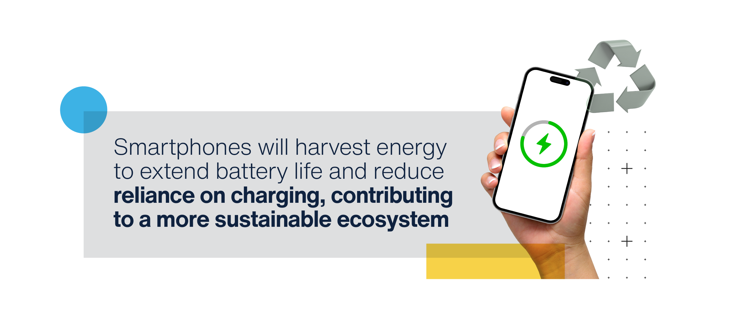
With the need to remain as portable as possible, however, this means that the additional performance must be matched with improved energy efficiency and a significant improvement in battery life. Ultimately, smartphones will use a combination of many of the techniques described above to optimize device performance while harvesting energy to extend battery life, reducing the reliance on regular charging and contributing to a more sustainable ecosystem. The silver screen vision of smartphones and mobile devices that never need charging may still be a way off, but the ability to access peak performance without an anxious search for a power source is within reach.
The post Power in Motion: how self-charging phones will quite literally put power in consumer’s hands appeared first on ELE Times.
Wolfspeed appoints former NXP and ams OSRAM executive Gregor van Issum as CFO
Hardware alterations: Unintended, apparent advantageous adaptations

After many (many) years of resisting temptation, followed by sowing seeds via succumbing to irresistible, gently-used-on-eBay prices for both generations of Schiit’s Mani phono preamp:

I’ve recently reconnected with the “vinyl” infatuation of my youth. Sorry, audiophiles, you’re still not going to convince me that records “sound better” than lossless (in reality, preferably perceptibly, minimally), large sample size, and high sample rate digital files, whether locally stored or Internet-streamed. In my contrarian opinion, in fact, the claimed “warmth” of the stylus (aka, “needle”)-delivered music is fundamentally a reflection of its measurably degraded SNR and other distortion measures versus more pristine digital alternatives, akin to guitar players clinging to archaic amp-and-speaker sets and recording engineers preferring ancient mics.
So why have I gone back “down the rabbit hole”, then? It’s because, access inconvenience (vs digital) aside, there’s something fundamentally tactile-titillating and otherwise sensory-pleasing (at least to a memory-filled “old timer” like me) to carefully pulling an LP out of its sleeve, running a fluid-augmented antistatic velvet brush over it, lowering the stylus onto the disc and then sitting back to audition the results while perusing the album cover’s contents. I’m not going to admit publicly how many (dozen) albums I’ve already accumulated while also striving to suppress ruminations on the dozens of albums I donated a few dozen years ago. I’ve also acquired several turntables, both belt- and direct-drive in design, which I’ll assuredly be showcasing in future write-ups.
The two turntablesThe first, Audio-Technica’s AT-LP60XBT, is the star of this piece:

My wife actually bought the AT-LP60XBT for me a while ago, along with a rare, sealed copy of “Buckingham Nicks,” Lindsey Buckingham, and Stevie Nicks’ only album prior to joining Fleetwood Mac. I finally dug it out of storage and fired it up earlier this year. Audiophiles are both cringing and chuckling at this point because it’s admittedly an entry-level model, both in comparison to upscale options from Audio-Technica’s own product line (that latest transparent turntable is wild, eh?) and examples from other manufacturers—my Fluance RT85, for example:

That said, it’s fully automatic in operation, which is great when we just want to listen to music, not bothering with the added minutia of manually placing the stylus on the disc prior to playing it and then returning the headshell (along with its mated tonearm) to rest afterward. And, referencing the “BT” portion of the product name, the AT-LP60XBT’s inclusion of both wired (albeit not with user-selectable integrated preamp bypass support for an external preamp such as one of the Schiit units mentioned earlier, a feature which its AT-LP70XBT successor offers) and wireless over both SBC and higher quality albeit baseline aptX Bluetooth codecs (audiophiles out there are really cringing now) affords it expanded connectivity and location flexibility.
Cartridge optionsOne key reason why the AT-LP60XBT is viewed as an “entry-level” turntable (aka, “record player”) is that it doesn’t support user upgrade of the (also entry-level) cartridge that originally came with it. Then again, that same inflexibility also means that AT-LP60XBT owners never need to bother with tracking force and antiskating control settings. The topics of cartridges and the styli they mate with, I quickly learned upon reconnecting with turntable technology, provide no shortage of opinions, debate, disagreement, and diatribes within the “vinyl” community.
Two main cartridge options exist: moving magnet and higher-end moving coil. They work similarly, at least in concept: in conjunction with the paired stylus, they transform physical info encoded onto a record via groove variations into electrical signals for eventual reproduction over headphones or a set of speakers. Differences between the two types reflect construction sequence variance of the cartridge’s two primary subsystems—the magnets and coils—and are reflected (additionally influenced by other factors such as cantilever constituent material and design) not only in perceived output quality but also in other cartridge characteristics such as output signal strength and ruggedness.
Stylus optionsOnce you’ve selected a particular cartridge technology, manufacturer, and model, you then need to pick the stylus (or styli…keep reading) for that cartridge. Again, two primary needle heads (the tip of the stylus, which makes contact with the record groove) types—conical and elliptical—exist, a topic which I’ll discuss in more detail shortly, but other, higher-end (at a much higher cost) options are also available. And then there are both nude (solid diamond) and bonded (metal with a diamond tip) needle construction options…terminating in either a round or square stylus shank…it’s enough to cause a headache. I’d even read about turntable owners who keep at close reach multiple styluses (and even cartridges, for the true fanatics) options for on-the-fly interchange, depending on what disc is to be played next! Therefore, I guess, another advantage to the AT-LP60XBT: fewer options (and combinations of them) to fuss about. Hold that thought.
As previously mentioned, the cartridge in this case (a variant of the AT3600L) is permanently integrated with the headshell (which is also permanently integrated with the tonearm):

The included ATN3600LC stylus is conical, with characteristics Audio-Technical describes thusly:
A good all-rounder, literally. Its head is rounded with a radius of around 0.6 mil which touches the centre of the record groove walls, though 78 RPM records will need a much larger needle. Conical styli are often more budget friendly, producing a rich, solid sound.

Here’s, from Fluance, a conceptual picture of what the conical needle head looks like in-groove:

Styli eventually wear out and need to be replaced:

And for alternative upgrade (at the tradeoff of shorter usable life prior to needed replacement), Audio-Technica also offers an elliptical stylus, the ATN3600LE, for the AT3600L cartridge:

Here’s how Audio-Technica describes the underlying elliptical needle head technology:
The front part of the needle rides in the center of the record groove, while the smaller side makes more contact with the groove walls. This helps produce a more enveloping sound, as an Elliptical stylus tracks the vinyl grooves with greater precision.
Again, from Fluance, here’s an in-groove conceptual image for the elliptical needle head:

And here’s Fluance’s broader “take” on differences between various cartridge and styli options:
That said, my research had also uncovered recommendations for two elliptical stylus alternatives to the ATN3600LE for the AT3600L; the comparably priced LP Gear CFN3600LE:

and lower cost (albeit, from my research, functionally equivalent) Pfanstiehl 4211-DE:

I, of course, went with the cheaper $29 option 
Once I had both styli in my hands, I did audition comparisons between them on several pristine LPs typifying various music genres. Did I discern any differences? Not really, honestly. That said, my listening approach was admittedly casual, not critical. And again, the cartridge and broader turntable are entry-level. So, did that mean I’d wasted $29? Not at all, as it turned out.
The key word here is pristine. Most of the vinyl I’ve so-far acquired has been brand new, so that I don’t inherit the previous owner’s (or owners’) extended listening and potential poor handling wear-and-tear outcomes. But in a few cases, I’ve gone with used purchases for reasons such as:
- The album’s no longer in “pressing” production, so any (if at all) remaining new copies are outrageously expensive (example: Widespread Panic’s Light Fuse, Get Away), or
- On the other end of the spectrum, I might have come across a used copy whose vs-new low price I’d been unable to resist, so I’d decided to roll the dice and take a chance.
Take, for example, Rush’s Archives, a compilation of the band’s first three albums, Rush, Fly By Night, and Caress of Steel. The latter two standalone titles currently sell new for ~$30 each on Amazon; judging from scant and pricey ($138!) new inventory there, I suspect Rush is no longer in production. I can’t find Archives new on Amazon; on eBay, it’s selling (again, new) for $249 and up. Conversely, on Mercari (no, I never learn) I’d found a cosmetically decent (judging from photos and descriptions) copy for $22.95 minus a 10% promo coupon (plus shipping and tax).
I went for it. When it arrived, alas, it suffered from no shortage (albeit also not a superfluous amount) of “clicks” and “pops”, in spite of my diligent cleaning attempts. Disc two, unfortunately, also had a notable skip right in the middle of the eponymous title track. The apologetic seller offered me a $10 partial refund, which helped. That said, there still was the matter of the Fly By Night flaw. But then I remembered something else mentioned in my earlier stylus research.
Because conical styli only ride partway down in the record groove, they supposedly don’t capture all the available fidelity potential with pristine records. But that same characteristic turns out to be a good thing with non-pristine records, for which all manner of gunk has accumulated over time in the bottom of the groove. By riding above the dross, the conical needle head doesn’t suffer from its deleterious effects.
I glanced at the cartridge: yep, I had the elliptical stylus installed. I swapped it out for the conical counterpart: notably fewer “clicks” and “pops”. And apparently that same “lack of precision” also makes a conical stylus more immune to even more egregious groove flaws, because the skip was now completely gone, too. Prior sarcasm thus humbled by subsequent experience to the contrary, I now “keep at close reach both stylus options for on-the-fly interchange depending on what disc is to be played next.” With no shortage of associated chagrin. Ahem.
Lessons learnedWhy’d I tell this tale? Because, at least to me, it’s not just about turntable styli. As I thought back on the experience afterward, I realized that it more broadly exemplifies a situation that many of you (and certainly I) have likely experienced during past product development cycles. You make a design tweak, maybe just to save a few cents on the bill-of-materials cost. It delivers the desired outcome…or maybe it doesn’t. But inevitably, it also results in other (often ahead of time unforeseen) transformations to the product you’re working on, sometimes for the better, sometimes for the worse, and sometimes just making it different.
What situations like mine have you encountered in the past, and how have they informed your subsequent product development (and broader tactics-for-life) approaches? Let me and your fellow readers know in the comments!
—Brian Dipert is the Editor-in-Chief of the Edge AI and Vision Alliance, and a Senior Analyst at BDTI and Editor-in-Chief of InsideDSP, the company’s online newsletter.
Related Content
- Mega-cool USB-based turntable
- Vinyl vs. CD: Readers respond
- Audio myth: Vinyl better than CD?
- Vinyl vs. CD: More reader feedback
- Vinyl vs. CD myths refuse to die
The post Hardware alterations: Unintended, apparent advantageous adaptations appeared first on EDN.
Нова послуга бібліотеки КПІ "Стюард даних"

У березні 2025 року Науково-технічна бібліотека КПІ запропонувала дослідникам нову послугу "Стюард даних" (https://www.library.kpi.ua/open-science/styuard-danyh/).
Її впровадження стало можливим завдяки участі КПІ ім. Ігоря Сікорського у проєкті Erasmus+ Open4UA – Відкрита наука для системи вищої освіти.
Handle with care: Power and perils of compound semiconductors

In the realm of advanced electronics and photonics, compound semiconductors are the silent enablers of breakthrough performance in many applications. Built from materials like indium gallium arsenide (InGaAs) or gallium arsenide (GaAs), these semiconductors enable applications that are beyond the capabilities of silicon devices.
Examples include avalanche photodiodes (APDs) for ultra-sensitive infrared detection at eye-safe wavelengths. These are used in LiDAR, optical test equipment, optical communications, and laser range finders, for example.
But as useful as they are, APDs made from compound semiconductors have some vulnerabilities, all of which can be mitigated through careful storage, handling, and application. Handle them with care, and you will avoid compromised performance, reduced lifespan, or complete failure.
Here’s what you need to know to ensure these components give their best.

Figure 1 Compound semiconductors have unique characteristics that can lead to vulnerabilities, but all of these can be mitigated with appropriate storage, handling, and application. Source: Phlux Technology
Why compound semiconductors are more fragile than silicon
Compared to silicon, compound semiconductors are physically and chemically more delicate. Their crystal structure makes them brittle, so they’re more likely to crack or chip if dropped or mishandled. Chemically, they’re also more reactive, exposing them to moisture, dust, or skin oils can lead to surface degradation, which affects performance.
They also struggle with heat. Lower thermal conductivity and mismatched coefficients of expansion make them vulnerable to thermal shock. Moreover, poor soldering practices or rapid temperature changes can cause delamination or internal fractures. And because many compound semiconductor APDs operate at low voltages and high impedance, they’re exceptionally sensitive to electrostatic discharge (ESD). A tiny static zap, invisible to you, might silently destroy the device.
APDs: Your handling survival guide
- Watch out for static
ESD isn’t just a nuisance, it’s a silent killer. Always handle APDs in an ESD-safe environment. That includes grounded workbenches, wrist straps, anti-static mats, and maintaining relative humidity between 40–60% to prevent static buildup. Keep the devices in anti-static packaging until you’re ready to use them.
- Handle with a gentle touch
APDs are inherently a little fragile. Use appropriate tools such as tweezers or vacuum pickups and handle the correct areas: the can for TO-CAN packages, the edges for SMDs, and the ferrule (never the fiber) for fiber-pigtailed versions. Never apply pressure to the photosensitive area or exposed wire bonds.
Contamination, whether from skin oils or airborne particles, can degrade signal integrity, so wear gloves and work in cleanroom or semi-clean environments. If cleaning is necessary, use approved solvents or dry nitrogen with extreme care.
- Beware the heat
Thermal stress is one of the top killers of compound semiconductors. Always follow recommended soldering profiles using gradual temperature ramps to prevent cracking or delamination. Preheat boards before reflow soldering and allow cooling to happen slowly. Desoldering is especially risky because temperatures above 330°C, even for just a few seconds, can irreparably damage many APD packages.
- Store them smart
APDs are sensitive even when idle. Store them between 5°C and 30°C, with relative humidity below 60%. Use moisture-barrier bags with desiccant packs and humidity indicators whenever possible. If you remove them from their original packaging, ensure the alternative provides equivalent ESD and moisture protection.
For SMD APDs, pay close attention to their moisture sensitivity level (MSL). Devices stored for extended periods—especially over a year—should be visually inspected and electrically tested before use. And if the MSL safe exposure window has been exceeded, follow proper bake-out procedures before reflow soldering.
Package-specific recommendations
- TO-CAN APDs
These are relatively robust but not invincible. The transparent window is critical for light transmission and must be kept clean and scratch-free. Avoid applying excessive mechanical force to the can, and ensure mounting solutions (sockets, clips, or heat sinks) don’t stress the package. Good thermal management is especially important when operating at high optical power or bias voltage.

Figure 2 Even TO-CAN packaged APDs need careful handling, so it’s important to keep transparent windows clean and scratch-free. Source: Phlux Technology
- SMD APDs
These are compact and efficient, but they come with stricter handling requirements. Many come under MSL 2 or MSL 3 classifications, meaning they must be soldered within a limited time after exposure to air. If that window closes, you’ll need to bake them before soldering. Stick to soldering temperatures between 270–300°C and avoid brief spikes above 330°C.
- Fiber-pigtailed APDs
These versions come with an optical fiber attached, and the fiber is the most delicate part of the assembly. Never bend it below its minimum bend radius and always protect the end-face with a dust cap or ferrule cover. Even minor contamination at the tip can cause significant optical loss or permanent damage.
Best practices summary
- Use strict ESD precautions at every stage of handling.
- Avoid mechanical shocks, bending, or applying pressure in the wrong places.
- Store APDs in controlled temperature and humidity environments with proper packaging.
- Follow soldering guidelines carefully, including reflow and desoldering profiles.
- Keep optical fibers clean and protected from strain or contamination.
APDs built from compound semiconductors are extraordinary components and enablers of much of the technology we take for granted today. However, they also require more attention than their silicon-based cousins. If you handle them with the precision they deserve, you’ll be rewarded with reliable, high-quality results.
If not, the damage might not show up immediately but rear its head later. Handle with care to reap the full benefits of these devices, including those of the world’s most sensitive 1550-nm noiseless InGaAs APD sensors.
 Christian Rookes is VP of marketing at Phlux Technology, a manufacturer of avalanche photodiode (APD) infrared sensors based in Sheffield, UK. He has over 25 years’ experience in technical marketing in semiconductors and optical communications. He holds two patents, including one related to impedance matching for laser diode circuits.
Related Content
- Photodiode Design Note
- Photodiodes and other Light Sensors, Part 1
- Photodiodes and other Light Sensors, Part 2
- Imec Taps Pinned Photodiode to Build a Better SWIR Sensor
- Avalanche Photodiode Innovations Target LiDAR Cost Challenges
The post Handle with care: Power and perils of compound semiconductors appeared first on EDN.
NPN Transistors Used as High-Side Switches (Photocouplers)
") | Just sharing a bit of a personal epiphany. While browsing through some old schematics at work as reference for a new design, I saw these photocoupler circuits with the NPN transistor outputs used as a high-side switch. I thought to myself "this design can't be right!" and after some research found the below documentation. The base is left floating and some magic from how the LED light affects the phototransistor section causes current to flow from the collector through the base which allows the NPN output to be used for both low-side or high-side configurations. Mind Blown. If anybody knows more about how the magic works, I'd love to read up. How Photocouplers / Optocouplers Are Used [link] [comments] |
eevBLAB 130 - Youtube Are FINALLY Demonetising AI Slop Channels?
Just bought this kit to make a speaker !
 | Found this on AliExpress so I don’t know how good it will be. But I’m learning electronics and electrical engineering so I think this will be a good easy project. [link] [comments] |
Hologram RGB
 | submitted by /u/weirdape [link] [comments] |
Not as crazy as some other projects here, but I wanted to share my first step into the digital world :)
") | submitted by /u/NSpeed__ [link] [comments] |
Pages


![[link]](https://i.redd.it/7umbk3wrqcbf1.jpeg)
![[link]](https://i.redd.it/xi02bor9qbbf1.jpeg)