
Feed aggregator
ASDC Conclave 2025: Accelerating Tech-Driven Skilling for Future Mobility
Automotive Skills Development Council (ASDC) hosted its 14th Annual Conclave 2025, themed “Stronger Together, Transform Tomorrow”, bringing together leaders from government, industry, and academia to deliberate on the future of skilling in the automotive sector.
The event commenced with the traditional lamp lighting ceremony. F.R. Singhvi, President, ASDC, presented the Annual Update, highlighting the Council’s 2024–25 impact—key achievements included forging partnerships with universities, advancing women’s skill development and employment, strengthening industry–academia collaboration, and expanding its international footprint. This was followed by addresses from the Guests of Honour: C.S. Vigneshwar (President, FADA), Shradha Suri Marwah (CMD, Subros Limited & President, ACMA), C.V. Raman (CTO, Maruti Suzuki India Ltd.), and Dr. Vinita Aggarwal, IES (Retd.), Executive Member, NCVET.
C.V. Raman, CTO, Maruti Suzuki India Ltd, emphasized that India’s mobility future will be driven by advanced engineering, digitalization, and disruptive technologies such as EVs, IoT, and AI. To realize the $5 trillion vision, he stressed the need for skilling to evolve by integrating experiential learning, fostering industry–academia collaboration, and leveraging startup innovation.
Dr. Vinita Aggarwal highlighted the importance of qualification standardization, stating: “India’s journey to becoming a global skill hub is powered by standardization and industry alignment. With over 180 automotive QPs under NSQF, we must ensure they remain dynamic—integrating hands-on training, apprenticeships, and micro-credentials. The automotive sector should actively adopt and upgrade these QPs to build a future-ready, tech-driven workforce.”
Speaking at the conclave, F R Singhvi, President, ASDC, remarked: “This conclave has reinforced our belief that India’s skilling ecosystem thrives on partnerships. Together, we are shaping a workforce that is not only job-ready but future-ready.”
A major milestone of the conclave was the release of a White Paper and the signing of MoUs with Hero MotoCorp, Bajaj Auto, Gandhi Auto, Delphi TVS, and Bosch India to scale up skilling initiatives nationwide.
The conclave also hosted two high-impact panel discussions: Academic Excellence to Industry Impact: Aligning Talent Pipelines with Future Mobility Technologies and From Garage to Gigabyte: Skilling for Next-Gen Automotive Technologies. These sessions examined how new-age skilling can bridge classroom learning with the demands of digital-first, tech-driven automotive industries.
Vinkesh Gulati, Vice President, ASDC, added: “Our collective responsibility is to ensure that every young aspirant finds a place in the industry’s growth story. ASDC is committed to bridging the gap between potential and opportunity.”
The Certified Candidates Convocation felicitated skilled candidates from ASDC’s flagship programs, underscoring its commitment to inclusive skill development. Presentations on CSR Best Practices by Bajaj Auto and Hero MotoCorp Ltd. showcased impactful industry-led skilling models. Recognitions included Internationally Placed Candidates, Rewards & Recognition Awards, and the ASDC Excellence and Special Recognition Awards, celebrating exemplary contributions to the skilling ecosystem.
The conclave firmly reiterated that public-private partnerships will be the cornerstone in addressing the evolving needs of the automotive industry and enabling India to emerge as a global leader in mobility technologies.
The post ASDC Conclave 2025: Accelerating Tech-Driven Skilling for Future Mobility appeared first on ELE Times.
Making your architecture ready for 3D IC

The landscape of IC design is experiencing a profound transformation. With the physical and economic limits of conventional two-dimensional scaling, the industry is rapidly embracing three-dimensional integrated circuits (3D IC) to unlock higher performance, lower power consumption, and denser silicon utilization.
For semiconductor professionals, understanding the distinct nuances of 3D IC microarchitectures is no longer optional. It’s becoming essential for those seeking to maintain a competitive edge in next-generation system design.
Microarchitecting in the 3D IC era represents more than an incremental change from traditional practices. It entails a fundamental redefinition of how data and controls move through a system, how blocks are partitioned and co-optimized across both horizontal and vertical domains, and how early-stage design decisions address the unique challenges of 3D integration.
This article aims to provide essential context and technical depth for practitioners working toward highly integrated, efficient, and resilient 3D IC systems.

3D IC technology now stands at a pivotal juncture. Source: Siemens EDA
Putting things in context
To grasp the impact of 3D IC, it’s crucial to define microarchitecture in the IC context. System architecture typically refers to a design’s functional organization as seen by software engineers—abstract functions, data flows, and protocols. Microarchitecture, viewed through the hardware engineer’s lens, describes how those features are realized in silicon using components like register files, arithmetic logic units, and on-chip memory.
Microarchitecture centers around two domains: the datapath, which encompasses the movement and transformation of data, and the control, which dictates how and when those data movements occur. Together, they determine not only performance and efficiency but also testability and resiliency.
Furthermore, while traditional ICs optimize microarchitecture in two dimensions, 3D ICs require designers to expand their strategies into the vertical axis as well. Because data in 3D ICs no longer flows only laterally, it must be orchestrated through stacked dies, each potentially featuring its own process technology, supply voltage, or clock domain. Inter-die communication—typically realized with micro-bumps, through-silicon vias, or hybrid bonding—becomes critical for both data and control signals.
With the move toward submicron interconnection pitches, design teams must address tighter integration densities and the unprecedented task of partitioning logic and memory across multiple vertical layers. This process is not unlike assembling a three-dimensional puzzle.
Effective microarchitecture in this context demands careful co-optimization of logic, physical placement, routing, and inter-die signaling—with far-reaching implications for system latency, bandwidth, and reliability.
Moreover, some microarchitectural components can be realized in three dimensions themselves. Stacked memory sitting directly above compute units, for example, enables true compute-in-memory subsystems, affecting both density and performance but also introducing significant challenges related to signal integrity, thermal design, and manufacturing yield.
Taking complexity to the third dimension
A major trend shaping modern IC development is the shift toward software-defined silicon, where software can customize and even dynamically control hardware features. While this approach provides great flexibility, it also increases complexity and requires early, holistic consideration of architectural trade-offs—especially in 3D ICs, where the cost of late-stage changes is prohibitive.
The high costs of 3D IC design and manufacturing in general demand an upfront commitment to rigorous partitioning and predictive modeling. Errors or unforeseen bottlenecks that might be addressed after tape-out in traditional design can prove disastrous in 3D ICs, where physical access for rework or test is limited.
It is thus essential for system architects and microarchitects to collaborate early, determining both physical placement of blocks and the allocation of functionality between programmable and hardwired components.
This paradigm also introduces new questions, such as which features should be programmable versus fixed? And how can test coverage and configurability be extended into the post-silicon stage? Design teams must maintain a careful balance among performance, area, power, and system flexibility as they partition and refine the design stack.
Among the most significant physical challenges in 3D integration is the sharp increase in power density. Folding a two-dimensional design into a 3D stack compresses the area available for power delivery, while escalating local heat generation. Managing thermal issues becomes significantly more difficult, as deeper layers are insulated from heat sinks and are more susceptible to temperature gradients.
Test and debug also become more complex. As interconnect pitches shrink below one-micron, direct probing is not practical. Robust testability and resilience need to be designed in from the architecture and circuit level, using techniques like embedded test paths, built-in self-test, and adaptive power management long before finalization.
Finally, resiliency—the system’s ability to absorb faults and maintain operation—takes on new urgency. The reduced access for root-cause analysis and repair in 3D assemblies compels development of in-situ monitoring, adaptive controls, and architectural redundancy, requiring innovation that extends into both the digital and analog realms.
The need for automation
The complexity of 3D IC design can only be managed through next-generation automation. Traditional automation has centered on logic synthesis, place and route, and verification for 2D designs. But with 3D ICs, automation must span package assembly, die stacking, and especially multi-physics domains.
Building 3D ICs requires engineers to bridge electrical, thermal, and mechanical analyses. For instance, co-design flows must account for materials like silicon interposers and organic substrates. This necessitates tightly integrated EDA tools for early simulation, design-for-test verification, and predictive analysis—giving teams the ability to catch issues before manufacturing begins.
System heterogeneity also sets 3D IC apart. Diverse IP, technology nodes, and even substrate compositions all coexist within a single package. Addressing this diversity, along with long design cycles and high non-recurring engineering costs, demands multi-domain, model-based simulation and robust design automation to perform comprehensive early validation and analysis.
Meanwhile, traditional packaging workflows—often manual and reliant on Windows-based tools—lag far behind the automated flows for silicon IC implementation. Closing this gap and enabling seamless integration across all domains is essential for realizing the full promise of 3D IC architectures.
The evolving role of AI and design teams
As system complexity escalates, the industry is shifting from human-centered to increasingly machine-centered design methodologies. The days of vertical specialization are yielding to interdisciplinary engineering, where practitioners must understand electrical, mechanical, thermal, and system-level concerns.
With greater reliance on automation, human teams must increasingly focus on oversight, exception analysis, and leveraging AI-generated insights. Lifelong learning and cross-functional collaboration are now prerequisites for EDA practitioners, who will require both broader and more adaptable skillsets as design paradigms continue to evolve.
Artificial intelligence is already transforming electronic design automation. Modern AI agents can optimize across multiple, often competing, objectives—proposing floorplans and partitioning schemes that would be unfeasible for manual evaluation. Looking ahead, agentic AI—teams of specialized algorithms working in concert—promise to orchestrate ever more complex design sequences from architecture to verification.
Building failure resilient systems
As the boundaries between architectural roles blur, collaboration becomes paramount. In a world of software-defined silicon, architects, microarchitects, and implementation engineers must partner closely to ensure that design intent, trade-offs, and risk mitigation are coherently managed.
Real-world progress is already visible in examples like AMD’s 3D integration of SRAM atop logic dies. Such hybrid approaches demand careful analysis of read and write latency, since splitting a kernel across stacked dies can introduce undesirable delays. Partitioning memory and processing functions to optimize performance and energy efficiency in such architectures is a delicate exercise.
Heterogeneous integration also enables new microarchitectural approaches. High-performance computing has long favored homogeneous, mesh-based architectures, but mobile and IoT applications may benefit from hub-and-spoke or non-uniform memory access models, requiring flexible latency management and workload distribution.
Adaptive throttling, dynamic resource management, and redundancy strategies are growing in importance as memory access paths and their latencies diverge, and architectural resiliency becomes mission critical.
As failure analysis becomes more complex, designs must include real-time monitoring, self-healing, and redundancy features—drawing upon proven analog circuit techniques now increasingly relevant to digital logic.
Thermal management presents fresh hurdles as well: thinning silicon to expose backside connections diminishes its native lateral thermal conductivity, potentially requiring off-die sensor and thermal protection strategies—further reinforcing the need for holistic, system-level co-design.
3D IC moving forward
3D IC stands at a pivotal juncture. Its widespread adoption depends on early, multi-disciplinary design integration, sophisticated automation, and a holistic approach to resiliency. While deployment so far has largely targeted niche applications, such as high-speed logic-memory overlays, 3D IC architectures promise adoption across more segments and vastly more heterogeneous platforms.
For industry practitioners, the challenges are formidable, including three-dimensional partitioning, integrated automation across disciplines, and entirely new approaches to test, debug, and resilience. Meeting these challenges requires both technical innovation and significant organizational and educational transformations.
Success will demand foresight, tight collaboration, and the courage to rethink assumptions at every step of the design cycle. Yet the benefits are bountiful and largely untapped.
 Todd Burkholder is a senior editor at Siemens DISW. For over 25 years, he has worked as editor, author, and ghost writer with internal and external customers to create print and digital content across a broad range of EDA technologies. Todd began his career in marketing for high-technology and other industries in 1992 after earning a Bachelor of Science at Portland State University and a Master of Science degree from the University of Arizona.
 Pratyush Kamal is director of Central Engineering Solutions at Siemens EDA. He is an experienced SoC and systems architect and silicon technologist providing technical leadership for advanced packaging and new foundry technology programs. Pratyush previously held various jobs at Google and Qualcomm as SoC designer, SoC architect, and systems architect. He also led 3D IC research at Qualcomm, focusing on both wafer-on-wafer hybrid bond and monolithic 3D design integrations.
Editor’s Note
This is the first part of the three-part article series about 3D IC architecture. The second part, to be published next week, will focus on how design engineers can put 3D IC to work.
Related Content
- 3D IC Design
- Thermal analysis tool aims to reinvigorate 3D-IC design
- Heterogeneous Integration and the Evolution of IC Packaging
- Tighter Integration Between Process Technologies and Packaging
- Advanced IC Packaging: The Roadmap to 3D IC Semiconductor Scaling
The post Making your architecture ready for 3D IC appeared first on EDN.
Top 10 Reinforcement Learning Algorithms
Reinforcement Learning (RL) algorithms represent a class of machine learning methodologies where an agent learns to make decisions through interactions with an environment. The agent gets feedback in the form of rewards or punishments bestowed on it for the actions it takes, and the overall objective is to maximize cumulative rewards through time. Differing from supervised learning, RL does not rely upon labeled data, but rather it learns from experience. Through trial and error, reinforcement learning excels at solving sequential decision-making problems across domains like robotics, gaming, and autonomous systems especially when using value-based algorithms that estimate future rewards to guide action.
Main types of Reinforcement Learning (RL) algorithms:
- Value-Based Algorithms
Value-based algorithms primarily work towards evaluating the potential benefits an action may have in a given condition while making a decision. Value-based methods usually learn a value function known as the Q-value, which specifies the expected reward in the future by taking a particular action in a certain state. The agent executes an action with the aim of maximizing this value. An example of such algorithms is the Q-Learning algorithm wherein Q-values are updated through the Bellman equation. More advanced versions are Deep Q-Networks (DQN) that approximate these values by using neural networks in high-dimensional environments such as video games.
- Policy-Based Algorithms
Policy-based algorithms directly learn a policy that maps states to actions without estimating value functions. These methods optimize the policy using techniques like gradient ascent to maximize expected rewards. They are particularly useful in environments with continuous action spaces. One popular example is REINFORCE, a Monte Carlo-based method. Another widely used algorithm is Proximal Policy Optimization (PPO), which improves training stability by limiting how much the policy can change at each update.
3. Model-Based Methods:
These algorithms learn the model and simulate the evolution of states from an initial state and finally an action. Once the dynamics model is learned, the agent can use it to simulate the future states and choose the best action without ever interacting with the real environment. This family of algorithms is very sample-efficient and suitable for cases where acquiring data is either very costly or risky. An example that revolutionized the field is MuZero, which learns the model and the policy without ever being given the rules of the environment;at the same time, it attains state-of-the art performance in Go, Chess, and other board games.
4. Actor-Critic Algorithms
Actor-Critic algorithms are a hybrid reinforcement learning technique that combine the advantages of both value-based and policy-based methods. Actor-critic methods maintain two perspectives: the actor decides what action to take, while the critic evaluates how good the action was by employing a value function. This idea of two perspectives given stability to the training process and fosters great performance. Examples of algorithms: Advantage Actor-Critic(A2C), Asynchronous Advantage Actor-Critic(A3C), and Soft Actor-Critic (SAC) These are typically used in continuous control problems such as in robotics and autonomous driving.
Examples of Reinforcement Learning Algorithms:
Some widely used RL algorithms are Q-Learning, Deep Q-Networks (DQN), Proximal Policy Optimization (PPO), and Soft Actor-Critic (SAC). Q-Learning is a basic algorithm that learns the value of actions in discrete environments. On the other hand, DQN uses deep neural networks to work with high-dimensional inputs such as images and videos. PPO is a policy-based algorithm known for its stability and efficiency in continuous control tasks and hence is often applied in robotics. SAC is an actor-critic method that uses entropy regularization to promote exploration and thus achieves a very good performance in brutally difficult environments.
Top 10 reinforcement learning algorithms:
- Q-Learning
Since it is a value-based algorithm, Q-Learning is ideal for discrete action spaces. It learns by receiving rewards with which it updates Q-values for optimal action-selection policy. This makes it ideal, for example, in simple setups such as grid-worlds or basic games.
- Deep Q-Network (DQN)
DQN is an extension of Q-Learning in which Q-values are approximated using deep neural networks, enabling it to handle high-dimensional inputs such as raw pixels. It has had a great impact on RL by offering a solution for agents to play Atari games straight from screen images.
- Double DQN
Double DQN improves DQN by reducing overestimation bias through decoupled action selection and evaluation, resulting in more stable learning.
- Dueling DQN
Dueling DQN extends DQN by splitting the state value estimation and action advantage estimation, which is particularly beneficial for problems with many similar actions.
- Proximal Policy Optimization (PPO)
PPO is a policy algorithm that is both stable and efficient. It employs a clipped objective to avoid sudden policy updates and thus performs well in continuous control tasks such as robotics and locomotion.
- Advantage Actor-Critic
Advantage Actor-Critic is policy and value learning combined, which makes it applicable to real-time decision-making in dynamic, multi-agent environments.
- Deep Deterministic Policy Gradient (DDPG)
DDPG is geared for continuous action spaces and employs a deterministic policy gradient algorithm. It’s best applied to tasks such as robotic arm control and autonomous vehicles, where accuracy matters when it comes to actions.
- Twin Delayed DDPG (TD3)
TD3 improves DDPG with the addition of twin critics to mitigate overestimation and policy update delay for improved stability. These features make it particularly suitable for high-precision control in difficult simulations.
- Soft Actor-Critic (SAC)
SAC promotes exploration with the incorporation of an entropy bonus to the reward signal. This allows the agent to strike a balance between exploration and exploitation, making it extremely sample-efficient and powerful in deep exploration-requiring environments.
- MuZero
MuZero is a model-based algorithm that learns an environment model without knowing its rules. It unifies planning and learning to deliver state-of-the-art performance on strategic games such as Chess, Go, and Atari, and it’s one of the most sophisticated RL algorithms to exist.
The post Top 10 Reinforcement Learning Algorithms appeared first on ELE Times.
Now, where's that diode?!
 | [Not mine] [link] [comments] |
SDVs, ADAS, and Chip Supply Chains- What to Expect at the 3rd e-Mobility Conference
As technology remains the perennial growth factor across all industries, the automotive sector is no exception to this phenomenon. Ranging from System-on-Chips (SoCs) to ADAS, modern-day automobiles have turned into machines driven by software and semiconductors. The integration of technology in automobiles has led to the emergence of modern-day connected and software-driven vehicles. As these vehicles hit the roads, it’s essential to highlight the breakthroughs, challenges, and opportunities they bring to the table.
The e-Mobility Conference returns for its third edition on September 17th, 2025, at BIEC, Bangalore, alongside electronica India and productronica India, serving as a platform for the industry to voice challenges, share concerns, explore opportunities, and highlight key breakthroughs and insights.
Click here to secure your free seat in the conference now!
In its 3rd edition, the conference is set to take up the theme “Silicon to Mobility: EVs’ Quantum Leap,” where the eminent speakers and moderators will discuss the semiconductor components of EVs in detail. The conversations and discussions would focus on issues ranging from composition, implementation, observations, and others. As the conference unfolds, it will look into some specific issues that present some substantial opportunities for the automotive industry.
One among them is the issue of standardization, where the panel would look into a wholesome integration and composition of semiconductors in EVs, keeping in mind the dynamics of the market and demand already in place. As the conference moves forward, the discussions over the composition and integration aspect will move into the subject matter of Software Defined Vehicles (SDVs), underlining how chips and software are transforming the way we perceive vehicles. It will talk about the emergence of SDVs and how this transformational shift is gradually pushing the ownership as well as after-sales revenue in the automotive sector.
In its later part, the conference would take up Advanced Driver Assistance System (ADAS) to discuss how data-driven decisions and command and control can prevent accidents on the road, enabling a safer and healthier automotive landscape in the country and worldwide. Finally, the conference would rise to discuss the conundrum of semiconductor supply chains and how geopolitics is getting heavily in the way as nations double down on trade barriers and global trade receives a jolt from some specific policies.
To witness all this firsthand for free and also get a chance to ask questions, register here!
As India and the world rise to adopt and embrace EVs, it becomes more important than ever to look into how we can shape these transformations to enable seamlessness and convenience for our people across the globe.
The post SDVs, ADAS, and Chip Supply Chains- What to Expect at the 3rd e-Mobility Conference appeared first on ELE Times.
Silicon Labs Debuts Sub-GHz Wireless SoC for Cost-Sensitive Designs
Working perfectly I'm sure...
 | Quite an interesting failure - not something I've seen before. For those interested, this is inside a PA amplifier, which surprisingly does still function, although this may be for the untested channel. PAT sticker from 2005 so at least 20 years old. [link] [comments] |
Ayar Labs and Alchip to scale AI infrastructure with co-packaged optics
Axcelis launches Purion Power Series+ ion implant platform for SiC power devices
Keysight Introduces Physical Layer Compliance Test Solution for HDMI Links
Enphase Energy opens US pre-orders for its first GaN-based microinverters
Infineon signs memorandum of understanding with China’s Lingji
Calculation of temperature from PRTD resistance

I recently contributed a design for a simple platinum resistance temperature detector (PRTD) resistance two-wire 4-20mA transmitter circuit illustrated in Figure 1.

Figure 1 A two-wire, 4 to 20 mA current loop PRTD transmitter with 500 µA constant current sensor excitation. R1 and R2 are 0.1% tolerance, voltage reference is a 2.5-V LM4040x25
Wow the engineering world with your unique design: Design Ideas Submission Guide
Analog to digital conversion of the 4 to 20 mA Io reading is likewise simple and straightforward (a 250-Ω shunt resistor at the input of a 0 to 5-V ADC of adequate resolution and precision will do nicely) and getting from there to Rprtd is an easy chore in software (Io in milliamps):
PRTD resistance = R1(Io/Ix – 1) = 20Io – 10
The final step from there to a linear temperature measurement would be almost equally easy, thanks to Callendar Van Dusen (CVD) math, except for one annoying detail. The famous CVD polynomial is arranged to calculate PRTD resistance from temperature. Unfortunately, what we need is temperature from resistance!
Fortunately, another classic algebraic expression can ride to our rescue: The Quadratic Formula (QF).
Mixing vigorously CVD and QF and defining two constants:
u = 0.0039083 RPRTD@0oC
w = -0.0000005775 RPRTD@0oC
and one new variable,
x = RPRTD@0oC – PRTD
leads to a straightforward polynomial that will directly calculate a PRTD temperature from PRTD resistance that’s linear to within ±0.05oC over a temperature range spanning -80oC to +850oC.
ToC= (-u + (u2 – 4wx)1/2)/(2w)
Stephen Woodward’s relationship with EDN’s DI column goes back quite a long way. Over 100 submissions have been accepted since his first contribution back in 1974.
Related Content
- Simple but accurate 4 to 20 mA two-wire transmitter for PRTDs
- A two-wire temperature transmitter using an RTD sensor
- Improved PRTD circuit is product of EDN DI teamwork
- The power of practical positive feedback to perfect PRTDs
- Hotwire thermostat: Using fine copper wire as integrated sensor and heater for temperature control
The post Calculation of temperature from PRTD resistance appeared first on EDN.
Electronica India 2025: “It isn’t about browsing gadgets, it’s about validating million-dollar CapEx and OpEx decisions with live demonstrations,” says CEO Bhupender Singh
India’s electronics and semiconductor sector is at an inflection point. With government-backed incentives like the Production Linked Incentive (PLI), Electronic Components Manufacturing Scheme (ECMS), Design Linked Incentive (DLI) schemes, global supply chains realigning toward India, and domestic demand projected to propel the industry to US$500 billion by 2030, the country is rapidly shifting from a consumption-led market to a global hub for innovation, manufacturing, and IP creation.
At the heart of this momentum are platforms like electronica India and productronica India, organized by Messe Muenchen India. Far more than trade shows, these events have evolved into strategic accelerators of industry growth. By convening policymakers, global investors, innovators, suppliers, and manufacturers under one roof, they drive not just dialogue but measurable outcomes—new partnerships, technology transfers, integrated supply chains, and policy-to-market translation that strengthen India’s electronics value chain.
In this exclusive conversation with the ELE Times, President IMEA (India, Middle East, Africa), Messe München, CEO, Messe Muenchen India, shares his vision of how these platforms are turning India’s complexity into opportunity. From conceptualising the India Semiconductor Conclave to expanding into dual editions across North and South India, Mr. Singh outlines how electronica India and productronica India are catalyzing India’s transition from a promising market to a first-choice global electronics manufacturing hub. His insights reflect not only the growth of the two pioneering exhibitions but also the story of a nation positioning itself at the centre of the world’s electronics and semiconductor future.
- Since electronica India and productronica India began in 2000, what do you see as the biggest missed opportunities in their India journey—and how are you ensuring those opportunities are now fully realized?
In many ways, electronica India and productronica India have been a true barometer of India’s electronics industry. Over the years, as the Indian industry navigated the electronics design, services, and manufacturing industries from inverted tax structures to duty-free components and the current push for semiconductors and passive components self-reliance, these shows have consistently highlighted the trending opportunities supporting the Indian industry’s requirements.
While India’s exponential growth and the rapid evolution from being a talent pool to a design and manufacturing powerhouse were faster than expected, it did attract global players who recognized India’s potential. We are capitalising on this opportunity by curating platforms that connect policy makers, investors, innovators, suppliers, and manufacturers under one roof. Through initiatives such as the India PCB Tech Conference, CEO Forum, etc., and stronger global partnerships, we are converting that complexity into structured opportunity.
These events are not just exhibitions; they are essential hubs driving dialogue, enabling policy alignment, and facilitating high-value business partnerships critical to India’s electronics roadmap.
- What is your vision for electronica India and productronica India in the next 5-7 years, and what concrete milestones will you use to measure whether that vision is being achieved?
Our vision is anchored in India’s national target of US$500 billion in electronics manufacturing by 2030. We firmly believe in supporting this goal and are confident that our shows will act as catalysts for this journey—not just by providing visibility but by accelerating deal-making, knowledge exchange, and policy adoption.
To achieve our vision and in a move that marks a strategic turning point for India’s electronics manufacturing sector, we are rolling out a two-edition model—annual editions of electronica India and productronica India in both Delhi-NCR and Bengaluru. Each of these regions has its own unique ecosystems, and the new format responds to clear industry demand: shorter sourcing cycles, stronger regional access, and more consistent face-to-face engagement.
Through these region-focused shows, we look to transform India from being primarily a consumption market to becoming a global hub for innovation, manufacturing, and IP creation. The shows are designed as confluences of ideas—where roadmaps are stress-tested, sourcing strategies redesigned, and partnerships sealed. Success will be measured across four milestones:
- Business Outcomes – Tangible trade volumes and partnerships generated through the shows.
- Global Participation – More Tier-1 semiconductor and electronics majors co-locating their R&D and design centres in India.
- Policy Engagement – Using the platform to bridge government missions with industry stakeholders.
- Sustainability impact – Where exhibitors demonstrate measurable progress on green manufacturing.
- electronica India is often called a symbol of India’s technological strength. Beyond scale and visibility, what makes the show truly competitive against global giants like CES or Computex?
electronica India and productronica India began over two decades ago as focused B2B trade platforms. Today, they’ve evolved into the country’s largest integrated events for electronic components, systems, applications, and production technologies. While the comparison with CES or Computex is flattering, the differentiation is clear. Those are consumer-tech showcases, and electronica India and productronica India are ecosystem shows from the ground up—focused on components, design, production, and manufacturing solutions.
Our competitive edge lies in our ability to align India’s electronics strengths with global supply-chain needs while creating an authentic “design-to-manufacture” narrative. It lies in the deep dive systems view we offer from semiconductors and embedded systems to SMT automation, inspection, EMS, and supply-chain solutions.
For decision-makers, this is not about browsing the future of gadgets; it’s about validating million-dollar CapEx and OpEx decisions with live demonstrations. Our shows are centre points where product roadmaps are stress-tested, sourcing strategies redesigned, and partnerships get inked.
Moreover, the shows are dual-purpose: fulfilling the domestic market’s aspirations while positioning India as a credible export and services base. This unique two-front approach—local growth with global integration—makes them competitive with, and in some ways complementary to, the world’s largest technology platforms.
- You’ve announced that electronica India and productronica India will now be held twice a year. Isn’t there a risk of diluting quality or splitting participation? How will you prevent electronica India and productronica India from becoming just another crowded trade show?
The fear of dilution is natural, but the reality is different. India’s electronics industry is expanding so rapidly that one annual event can no longer serve its needs. Due to our shows taking place only once in two years in each region, 80% of our buyers visited only local shows, due to which they were facing significant sourcing gaps. They were pleased to support the dual-edition approach because it allows them to target regional clusters, send larger teams, and gain sharper insights.
Similarly, 70% of our top buyers felt that this was the way forward to create sharper industry fulfilments, and it meant easier access without waiting two years for the platform to return to their region or traveling across the country.
With exhibitor numbers growing year on year, two shows will mean a more expansive platform to enable us to cater to the entire industry across verticals and categories.
We don’t see this as two smaller shows. We see it as a distributed national platform. Quality will be preserved through strict curation, serious exhibitors, targeted buyers, and knowledge-driven conferences. Instead of spreading thin, we are going deeper, closer to where the industry is growing.
Our role is not just to mirror market shifts but to actively shape the ecosystem by fostering collaborations that lead to tangible outcomes.
- India’s electronics manufacturing has grown rapidly, but critical areas like advanced semiconductors and IP creation still lag. How do electronica India and productronica India plan to attract global leaders in these domains rather than just showcasing assembly strength?
The challenge is not just manufacturing scale—it’s moving up the value chain. To bridge this, we are positioning electronica India and productronica India as knowledge-driven hubs.
We are focusing on knowledge partnerships and high-level policy dialogues to make India a dependable choice for global majors. Initiatives such as the e-Future Conference, the Smart Factory Innovation Conference, the India Semiconductor Conclave, and many more are curated specifically to attract global chipmakers, fabless design firms, and equipment suppliers to engage with India’s policy-makers and startups. It’s not about showcasing assembly strength; it’s about sparking IP creation and R&D investments.
By presenting live case studies, early-stage MoUs, and collaborative projects, we aim to send a clear signal: India is serious about semiconductors, and now is the time for global leaders to place their bets here.
- With India’s electronics growth driven largely by government incentives, how does electronica India and productronica India see its own role—as policy influencer, industry catalyst, or bridge to global investors?
We are all three. Government incentives create momentum, but unless they are translated into execution, their impact is limited.
- As a policy influencer, we host closed-door roundtables where industry challenges directly inform government priorities.
- As an industry catalyst, we enable knowledge transfer and create forums for startups, MSMEs, and global giants to collaborate.
- As a bridge to investors, we bring global capital face-to-face with India’s electronics ecosystem.
The true value of these shows lies in being the intersection point where policy intent, industry capacity, and investor confidence converge.
- Many exhibitors today are ROI-driven. What hard evidence can you present to prove that participation at electronica India and productronica India translates into business growth and not just visibility?
We track ROI rigorously, and the data speaks clearly. In 2024, over 70% of exhibitors reported promising agreements and serious leads. Similarly, SMEs closed technology transfer agreements, while larger corporates expanded supplier networks.
The electronica India and productronica India growth trajectory is equally telling, with participation numbers rising year on year. From 325 exhibitors in 2022 to 839 exhibitors in 2024, we have come a long way. This is a clear indicator of the exhibitors’ gains, encouraging them to return to our shows year on year.
Beyond deals, the shows deliver strategic ROI: direct access to policymakers, visibility with investors, increased brand awareness, and insight into emerging market intelligence. In a sector where supply-chain decisions lock in for years, those conversations are invaluable.
- With global supply chains undergoing overhaul changes, how can electronica India and productronica India position India as a genuine hub for electronics innovation and manufacturing, rather than merely a fallback option?
By providing evidence of India’s resilience, scalability, and talent depth. Through partnerships showcased at our events, the shows highlight India’s evolution beyond the “China+1” narrative to becoming a first-choice hub.
On the show floor, visitors see the future in action: modular automation, smart pick-and-place systems, automotive-grade board protection, energy-efficient reflow technologies, and MES-ERP integrated traceability stacks. These aren’t just demonstrations—they are proofs of capability that global buyers need to see before committing to India.
At the same time, startups and MSMEs bring grassroots innovation, while global OEMs demonstrate scale and reliability. The combination tells the world that India is not just supplying today—it is prototyping tomorrow.
- Is electronica India and productronica India’s vision to focus on fewer genuine, high-value participants or on sheer numbers, and how will you ensure quality isn’t diluted?
Our goal comprises depth and scale. In fact, the numbers present a clear picture as to why our shows are very well balanced in terms of quantity and quality. We not only attract return exhibitors but also new exhibitors year on year.
In 2022, we welcomed 20,942 visitors who interacted with 325 exhibitors. In 2023, we saw 39,133 visitors connect with 600 companies, and in 2024, over 45,532 visitors met with over 839 companies from 29 countries.
And in 2025, we are looking at an unprecedented 60,000 sqm of space hosting over 850 exhibitors from 50 countries, showcasing 6,000+ products and solutions. With 2,000+ curated B2B meetings sitting buyers and suppliers across the table with pre-matched interests, our shows are engineered for outcomes.
While visitor numbers will naturally rise with India’s booming electronics sector, our curation will focus on qualified buyers, decision-makers, and technology leaders. We invest heavily in hosted buyer programs, matchmaking tools, and pre-scheduled meetings, ensuring deal-focused interactions.
In a landscape where supplier decisions lock in multi-year costs, those hours are highly leveraged where every interaction has business value.
- Finally, what is your key message to the visitors and participating brands this year—and what specific commitments are you ready to make to them?
My message is simple: electronica India and productronica India 2025 are not just exhibitions—they are growth accelerators.
We are committed to delivering:
- Business-ready leads through curated matchmaking and buyer forums.
- Knowledge leadership through world-class conferences and global experts.
- Policy access, giving industry participants a direct voice in shaping India’s electronics future.
Every participant, whether a startup or a multinational, should leave with something tangible: a lead, a partnership, or a policy connection. We promise to make the 2025 editions not just the stage for India’s electronics growth, but the engine that powers it forward.
The post Electronica India 2025: “It isn’t about browsing gadgets, it’s about validating million-dollar CapEx and OpEx decisions with live demonstrations,” says CEO Bhupender Singh appeared first on ELE Times.
Scintil raises $58m to scale integrated photonics for AI factories
Top 10 Decision Tree Learning Frameworks
In machine learning, a decision tree learning framework is a method that is used to generate predictions from the data. The outcomes of the decision process are represented as leaf nodes in a tree-like structure. A tree node corresponds to a particular feature, while the branches correspond to the decision rules. Having arrived at the leaf nodes, an example is assigned an output by the framework. This framework is used for classification (like the prediction of categories) and regression (like the prediction of number values).
How Does the Decision Tree Learning Framework Work:
The algorithm starts with choosing the most appropriate feature to divide the dataset. The choice is made on the basis of factors such as Information Gain, Gini Impurity, or Entropy. The data is divided into subsets on the basis of the chosen feature. It is performed recursively over each subset until a condition of stopping is reached such as the achievement of maximum depth or pure leaf nodes. The outcome is a tree in which every root-to-leaf path is a decision rule.
Decision Tree Learning Framework Examples:
Decision tree learning is a well-known algorithm in machine learning for classification and regression. Libraries such as Scikit-learn, XGBoost, LightGBM, Spark MLlib, and rpart (in R) implement decision trees with ease. They are used in situations such as customer behavior prediction, disease diagnosis, loan approval, and spam detection where a decision is taken by dividing data along feature boundaries until a conclusion is derived.
Top 10 Decision Tree Learning Frameworks:
- TensorFlow Decision Forests
This framework brings decision tree models to the TensorFlow ecosystem. It addresses those wanting to work with tree-based models combined with deep learning workflows or for deployment of models in production through TensorFlow Serving.
- XGBoost
Short for “Extreme Gradient Boosting,” XGBoost is the one for structured data. This method builds ensembles of decision trees using gradient boosting and is apt for speed, regularization, and prowess on Kaggle competitions.
- Scikit-learn
The Python software library for machine learning, Scikit-learn, provides an elegant and intuitive implementation of decision trees using the CART algorithm. It is well suited for both beginners and experts, providing excellent documentation and the ability to integrate with other Python tools.
- LightGBM
By Microsoft, LightGBM is focused on speed. It uses histogram algorithms and growing trees leaf-wise, which is faster and more memory-efficient than traditional gradient boosting techniques, especially on huge datasets.
- H2O.ai
H2O contains implementations of Random Forest, Gradient Boosting Machines, and so forth, and does so at lightning speed. It’s enterprise-ready, supports parallel processing, and includes a user-friendly web interface for model building and evaluation.
- Apache Spark MLlib
Spark MLlib has been designed with distributed computing in mind, which means it supports scalable decision tree learning on clusters. This makes it ideal in big data environments, tightly integrated with the rest of the Spark ecosystem for complementary data processing.
- RapidMiner
This platform is more geared towards non-programmers, providing drag-and-drop capabilities for decision tree modeling. It is mostly commonly used for business analytics and supports integration with Python and R for more advanced users.
- WEKA
WEKA, a Java-based toolkit, is mostly used within academic fields for teaching and research. It provides a graphical user interface along with a number of machine learning algorithms, including decision trees, thus easing experimentation and visualization.
- CatBoost
Created by Yandex, CatBoost is one of the really few methods that can operate on categorical variables without transforming them into some numerical version. Because it is so robust now, quite accurate, and seldom requires extensive tuning, it has become a go-to method used in many real-world business cases.
- Orange
A visual programming toolkit for data mining and machine learning which contains decision tree learners, Orange is ideal for prototyping and academics. Its modular nature permits users to assemble workflows interactively without any form of programming.
The post Top 10 Decision Tree Learning Frameworks appeared first on ELE Times.
A little ehile ago I posted my very first Kicad designed morpho shield for stm32 nucleo microcontroller. Well, heres the final!
 | Hello everyone. This is the PCB I came up with. Its to simplify the setup of certain hardware laboratories controllers that I also came up with previously. Took me couple of days (around 4-5 hrs) of work to solder them all 40 boards. But this will make super easy to connect things, or replace the microcontroller in case of a failure. As my very first design (this is slightly revamped to add small "window" to see the status LED's on nucleo board), I once again, feel really proud, haha. The revamp also added another 6 blank pins for future expansion (there are plans to add dynamixel robot arms to controllable devices repertoire). [link] [comments] |
A digital technique eliminates the need for an analog multiplier

Traditionally, multiplying two analog signals involves the use of analog multipliers. Design engineers digitize analog signals using an analog-to-digital converter (ADC) and then run the code on a microcontroller to perform digital multiplication. However, another digital technique employing an XNOR logic gate alongside an ADC performs multiplication on two bitstreams, avoiding the cost of the analog multiplier.
Find out more about this substitute analog multiplication technique in an article published in EDN’s sister publication Planet Analog.
Related Content
- Simulating the front-end of your ADC
- Analog to Digital Converter (ADC) Basics
- Introduction to analog/digital converter (ADC) types
- Understanding analog-to-digital converter (ADC) drivers
- Analog-to-digital converter (ADC) accuracy in simple terms
The post A digital technique eliminates the need for an analog multiplier appeared first on EDN.
Reinforcement Learning Architecture Definition, Types and Diagram
Reinforcement Learning is a type of machine learning in which an agent learns to act by interacting with an environment, performing actions, and getting feedback in the form of reward or penalty. Rather than being instructed what to do, the agent finds out the optimum strategy by trial and error, trying to maximize cumulative rewards in the long run. It alternates between exploration of novel actions and exploitation of familiar good ones, adjusts according to changing circumstances, and frequently faces delayed rewards requiring long-term planning.
Reinforcement Learning Architecture is founded on a constant feedback cycle between an environment and an agent. The agent reads the state of the environment, selects an action based on its policy (its strategy for making decisions), and applies it. The environment reacts by changing to a different state and issuing a reward or penalty. As time progresses, the agent alters its policy based on this feedback to optimize long-term cumulative rewards. Key components are the policy (how to select actions), the value function (predicting future rewards), and possibly an environment model for planning.
Main types of Reinforcement Learning:
- Policy-Based Reinforcement Learning
Policy-based approaches bypass the value function and learn a policy directly, i.e., a mapping from states to actions. These approaches are especially beneficial for use in high-dimensional or continuous action spaces. They learn the policy with methods such as gradient ascent. REINFORCE and Proximal Policy Optimization (PPO) are examples of popular algorithms used in this category, providing stability and training efficiency.
- Model-Based Reinforcement Learning
Model-based methods consist of creating an environment model that estimates the next state and reward based on a current state and action. The agent utilizes this model to reason about future consequences and decide its actions. This approach is potentially more sample-efficient than model-free methods. Some examples are Dyna-Q, which combines planning and learning, and Monte Carlo Tree Search, applied in game-playing agents.
- Actor-Critic Methods
Actor-Critic methods combine the advantages of value-based and policy-based approaches. The actor selects what action to perform, and the critic judges how well the action was chosen through a value function. Double structure diminishes variance and enhances learning stability. A3C (Asynchronous Advantage Actor-Critic) and DDPG (Deep Deterministic Policy Gradient) algorithms are most commonly applied in continuous control problems.
Reinforcement Learning Architecture:
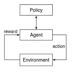
The diagram depicts the basic structure of a reinforcement learning system, showing how an agent learns to behave optimally by interacting with its environment. At the top, the policy determines the agent’s choices by mapping states to actions. The agent, shown centrally, applies this policy to choose an action that it then performs in the environment. The environment responds with a reward given in feedback form, which is an indication of the success of the performed action. This reward is fed back to the agent so it can modify its policy and make better decisions in the future. The policy of cyclical flow from agent to agent, agent to environment through action, and environment to agent through reward perfectly describes trial-and-error learning characteristic of reinforcement learning. Gradually, this cycle enables the agent to improve its plan and achieve maximum cumulative rewards through ongoing interaction and learning.
The post Reinforcement Learning Architecture Definition, Types and Diagram appeared first on ELE Times.
Didn't have the correct SMD component, nor the pertinence to wait.
 | Wanted to change the current limiting resistor on this DRV8871 motor driver board. Didn't want to wait for the correct component to used a through-hole resistor on 0603 pads. [link] [comments] |
Pages


![[link]](https://i.redd.it/zi0uv2wabaof1.jpeg)
![[link]](https://i.redd.it/guap1esi57of1.jpeg)
![[link]](https://i.redd.it/lvblik9st3of1.jpeg)