
Feed aggregator
“Robots are undoubtedly set to make the manufacturing process more seamless and error-free,” says Anil Chaudhry, Head of Automation at Delta.
“Everywhere. Automation can be deployed from very simple things to the most complicated things,” says Delta’s Anil Chaudhry as he underlines Delta’s innovations in the field of digital twins and human-centric innovation. With industries across the globe preparing to embrace the automation revolution—from advanced assembly lines to robotic arms—ELE Times sits down with Anil Chaudhry, Business Head – Solution & Robotics at Delta Electronics India, and Dr. Sanjeev Srivastava, Head of Industrial Automation at SBP, to discuss Delta’s plans.
In the conversation, both guests talk extensively about the evolution emerging in the industrial automation space, especially with reference to India, and how these solutions are set to support India in securing a significant share of the global semiconductor and electronics market. “The availability of the collaborative robots, or the co-bot, which is called in short form, is one of the stepping stones into Industry 5.0,” says Anil Chaudhry.
A Well-integrated and All-encompassing Approach
“We are in all domains, and we see these domains are well integrated,” says Anil Chaudhry as he reflects on the automation demands of the industry, ranging from power electronics to mobility (such as EV charging), automation (industrial and building automation), and finally the infrastructure (data centers, telecom & renewable energy). He highlights that such an approach makes Delta the most sought-after name in automation tech. “We offer products ranging from an AI-enabled energy management system to edge computing software that can handle the large, all-encompassing processes in an industrial landscape,” he adds.
“It is an integrated solution we have everywhere in our capabilities, and we are integrating all this to make it more enhanced,” says Anil Chaudhry.
Delta’s Key to Efficiency and Productivity
As the conversation touched upon the aspects of efficiency and productivity, Anil Chaudhry was quick to say, “The key to efficiency and productivity lies in no breakdown.” He further says that Delta’s software-enabled programs are equipped to provide predictive failure information to the manufacturing plant, enabling the necessary actions to be taken in advance.
Delta’s Stride through Digital Twins & Industry 5.0
Delta’s digital twin models imitate the manufacturing process, making it easy and seamless to enable automation. He says, “The robots are definitely going to enable the manufacturing process to be more seamless and more error-free. Sharing a glimpse into the Delta’s co-bots, he says that the robots are equipped enough to handle repetitive yet highly accurate and high-demand requirements.
He was quick to underline that Delta not only offers these machines but also a lot of software tools required to make the whole facility run seamlessly, making an end-to-end solution and enabling a stride towards an Industry 5.0 environment.
Delta’s Approach towards Localization
On the subject of localization of manufacturing in India, Dr. Sanjeev Srivastava, Head of Industrial Automation at SBP, highlighted the progress Delta has been making in building a strong ecosystem. “It’s good that we are developing an ecosystem wherein we also have our supply chain integrated with manufacturing, and as we see, a lot of industries are coming into India. Over the years, we will have a very robust supply chain,” he said.
He pointed out that many components are already being sourced locally, and this share is expected to grow further. Confirming Delta’s commitment to Indian manufacturing, Dr. Srivastava added, “Yes, we are manufacturing in India, and we are also exporting to other places. We have the global manufacturing unit, which is supplying to other parts of the world, as well as catering to our Indian market. So it is both domestic and international.”
As the conversation wrapped up, Anil Chaudhry went on to further underline Delta’s overall and larger goal, wherein he says, “So we work on the TC, or total cost of ownership, on how to reduce it with our technology going into the equipment, as well as the overall solution.”
The post “Robots are undoubtedly set to make the manufacturing process more seamless and error-free,” says Anil Chaudhry, Head of Automation at Delta. appeared first on ELE Times.
Звіт КПІ ім. Ігоря Сікорського зі сталого розвитку за 2024 рік
Aixtron’s Q3 revenue and margin impacted by volume shifts into Q4
Cornell’s Huili Grace Xing to receive 2025 University Research Award in Technology from SIA and SRC
NUBURU strengthens balance sheet, advances defense-tech acquisition program and revamps blue laser business
The Quantum Leap: How AI and Quantum Computing Are Driving Lead Time Optimization and Supply Chain Resilience in Semiconductor Innovation
Introduction
Silicon has been the primary driver of the computing growth for decades, but Moore’s Law is now reaching its limits. As the need for chips to be faster and more energy-efficient grows, the pressure on supply chains are like never before due to shortages and geopolitical tensions.
This is where AI and quantum computing come into play. It is not science fiction; they are
helping discover new semiconductor materials and optimizing production scheduling in
wafer fabs. This results in shorter lead times, reduced risks, and a more resilient supply chain.
For engineers and procurement teams, the message is simple: keeping up in the chip world
will soon require leveraging both quantum computing and AI together.
Quantum Computing and AI Integration in Semiconductor Innovation
Quantum computing works with qubits, which, unlike classical bits, can exist in
superposition, representing both 0 and 1 simultaneously. This enables quantum processors to tackle complex simulations that classical computers struggle with, such as modelling atomic-level behaviour in new semiconductor materials.
AI enhances this capability. By applying predictive analytics to quantum simulations,
machine learning models identify promising material candidates, predict their performance,
and recommend adjustments. This transforms what was once a slow trial-and-error process
into actionable insights, saving years of laboratory work.
Take Google’s Willow processor as an example. It is the follow-up to Sycamore, and while not built solely for materials research, it demonstrates how quantum systems can scale and
reduce errors. When combined with machine learning, it provides an unprecedented view of
material properties critical for chip innovation.
As Anima Anandkumar points out: “AI helps us turn the raw complexity of quantum
simulations into insights engineers can actually use.”- Anima Anandkumar, Professor,
Caltech & Senior Director of AI Research, Nvidia.
Together, AI and quantum computing are laying the foundation for a fundamentally new
approach to chip design.
AI-Driven Material Science: Operational and Market Impact
When it comes to discovering new semiconductors, atomic-level precision is crucial. AI-
powered quantum models can simulate electron behaviour in materials such as graphene,
gallium nitride, or perovskites. This enables researchers to evaluate conductivity, energy
efficiency, and durability before performing laboratory tests, greatly accelerating material
qualification.
The practical impact is significant. Material validation traditionally took years, but early
studies indicate that timelines can be shortened by 30 to 50 percent. This allows wafer fabs to operate more efficiently, align production with new innovations, and minimize idle time.
Market pressures further complicate the situation. During the 2021 shortage, lead times
increased from approximately 12 weeks to over a year. With AI, companies can anticipate
supply chain disruptions and proactively adjust sourcing strategies. Quantum simulations also expand the range of usable materials, reducing reliance on a single supplier or high-risk region.

Figure 1. Semiconductor lead times spiked from 12 weeks in 2020 to over 30 weeks in 2022 before easing. AI-quantum integration can help stabilize these fluctuations by enabling predictive analytics and diversified sourcing.
The return on investment is remarkable. According to Deloitte, companies that integrate AI
into R&D and supply chain operations are achieving double-digit efficiency gains, primarily due to improved yield forecasting and reduced downtime. Google’s quantum research team
has demonstrated that AI-driven simulations can narrow the list of promising materials from thousands to just a few within weeks, a process that would normally take years using classical computing. This dramatic compression of the R&D cycle fundamentally changes competitive dynamics.
Strategic Insights for Procurement and Supply Chain Leaders
For procurement and supply chain leaders, this is more than just a technical upgrade; it
represents a genuine strategic advantage. AI-powered quantum tools help optimize lead
times, enabling more precise supplier contracts and reducing the need for excess buffer stock. Predictive analytics also allow teams to identify potential risks before they affect wafer fabs or delay customer deliveries.
Supply chain resilience is also enhanced. When AI-guided quantum simulations confirm
alternative semiconductors that can be sourced from different regions, procurement teams
reduce exposure to geopolitical risks or natural disasters. This approach aligns with national
initiatives such as the U.S. CHIPS and Science Act and the EU Chips Act, both of which
promote stronger local production and more resilient sourcing strategies. Quantum-AI
modelling provides the technical confidence required to qualify these alternative supply
streams.
“The upward trajectory for the industry in the short-term is clear, but the companies that can manage their supply chains and attract and retain talent will be the ones well-positioned to sustain and benefit from the AI boom.”- Mark Gibson, Global Technology Leader, KPMG
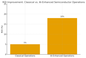
Figure 2. Firms adopting AI-enhanced semiconductor operations achieve significantly higher ROI, with consulting studies reporting double-digit efficiency gains compared to classical operations.
At the end of the day, companies that successfully integrate these technologies do not just
bring products to market faster; they also gain a genuine competitive edge in today’s unpredictable global markets. In the semiconductor industry, a delay of a few weeks can result in billions in lost revenue, so agility is essential for survival.
Future Outlook: Scaling Quantum AI Impact on Semiconductor Manufacturing
Looking ahead, the next major development appears to be full-stack quantum-AI design.
Imagine quantum processors running full-chip simulations while AI optimizes them for
speed, efficiency, and manufacturability. Although we are not there yet, incremental
advances in photonic circuits and spintronic components are already producing tangible
results.
For manufacturing teams, the challenge will be maintaining flexibility in supply chains. As
new materials move from simulation to pilot production, procurement and fab teams must
scale in coordination. Today’s quantum processors are not perfect, as they still face
limitations in qubit counts, error rates, and scalability, but if progress continues, practical
industrial applications could emerge within the next ten years. Companies that begin planning now, by developing roadmaps and forming strategic partnerships, will gain a significant advantage.
Conclusion
Right now, the semiconductor industry is at a critical turning point. Combining AI’s
predictive capabilities with quantum computing’s atomic-level insights can accelerate
discovery, shorten lead times, and make supply chains significantly more resilient.
For engineers and procurement leaders, the message is clear: adopting AI-quantum
integration is not just about technology; it is about remaining competitive. The next major
advancement in silicon will not occur by chance. It will be carefully designed, optimized, and engineered using AI and quantum computing together.
The post The Quantum Leap: How AI and Quantum Computing Are Driving Lead Time Optimization and Supply Chain Resilience in Semiconductor Innovation appeared first on ELE Times.
System-level tool streamlines quantum design workflows

Quantum System Analysis software, part of Keysight’s Quantum EDA platform, simulates quantum architectures at the system level. It unifies electromagnetic, circuit, and quantum dynamics domains to enable early design validation in a single environment.

By modeling the full quantum workflow—from initial design through system-level experiments—the software reduces reliance on costly cryogenic testing and shortens time-to-validation. It includes tools for optimizing dilution fridge input lines to manage thermal noise and estimate qubit temperatures. A time dynamics simulator models quantum system evolution using Hamiltonians derived from EM or circuit simulations, accurately emulating experiments such as Rabi and Ramsey pulsing to reveal qubit behavior.
Quantum System Analysis supports superconducting qubit platforms and can be extended to other modalities such as spin qubits. It complements Quantum Layout, QuantumPro EM, and Quantum Circuit Simulation tools.
The post System-level tool streamlines quantum design workflows appeared first on EDN.
CAN FD transceiver boosts space data rates

Microchip’s ATA6571RT radiation-tolerant CAN FD transceiver supports data rates to 5 Mbps for high-reliability space communications. Well-suited for satellites and spacecraft, it withstands a total ionizing dose of 50 krad(Si) and offers single-event latch-up immunity up to 78 MeV·cm²/mg at +125 °C.

Unlike conventional CAN transceivers limited to 1 Mbps, the ATA6571RT handles CAN FD frames with payloads up to 64 bytes, reducing bus load and improving throughput. It ensures robust, efficient data transmission under harsh space conditions, while backward compatibility with classic CAN enables an easy upgrade path for existing systems.
A cyclic redundancy check (CRC) algorithm enhances error detection and reliability in safety-critical applications. The transceiver also delivers improved EMC and ESD performance, along with low current consumption in sleep and standby modes while retaining full wake-up capability. It interfaces directly with 3-V to 3.6-V microcontrollers through the VIO pin.
The ATA6571RT transceiver costs $210 each in 10-unit quantities. A timeline for availability was not provided at the time of this announcement.
The post CAN FD transceiver boosts space data rates appeared first on EDN.
Reconfigurable modules ease analog design

Chameleon adaptive analog modules from Okika provide preprogrammed, ready-to-use analog functions in a compact 14×11-mm form factor. Each module employs the company’s FlexAnalog field-programmable analog array (FPAA) architecture—a reconfigurable matrix with over 40 configurable analog modules (CAMs), including filters, amplifiers, and oscillators. Nonvolatile memory and reconfiguration circuitry are integrated on the module.

Chameleon simplifies analog designs that need flexibility without the complexity of firmware or digital control. Modules function as fixed analog blocks straight out of the box—no microcontroller or firmware required. Configurations can be reprogrammed in-system or using any 3.3-V SPI EEPROM programmer.
Anadigm Designer 2 software provides parameter-tuning and filter-design tools for simulating and verifying Chameleon’s performance. Typical applications include programmable active filters, sensor signal conditioning and linearization, and industrial automation and adaptive control, as well as research and prototyping.
Chameleon extends the FlexAnalog platform into an application-ready design that adapts easily. For pricing and availability, contact sales@okikadevices.com.
The post Reconfigurable modules ease analog design appeared first on EDN.
Vertical GaN advances efficiency and power density

onsemi has developed power semiconductors based on a vertical GaN (vGaN) architecture that improves efficiency, power density, and ruggedness. These GaN-on-GaN devices conduct current vertically through the semiconductor, supporting higher operating voltages and faster switching frequencies.

Most commercially available GaN devices are built on silicon or sapphire substrates, which conduct current laterally. onsemi’s GaN-on-GaN technology enables vertical current flow in a monolithic die, handling voltages up to and beyond 1200 V while delivering higher power density, better thermal stability, and robust performance under extreme conditions. Compared with lateral GaN semiconductors, vGaN devices are roughly three times smaller.
These advantages translate to significant system-level benefits. High-end power systems using vGaN can cut energy and heat losses by nearly 50%, while reducing size and weight. The technology enables smaller, lighter, and more efficient systems for AI data centers, electric vehicles, and other electrification applications.
onsemi is now sampling 700-V and 1200-V vGaN devices to early access customers. For additional information about vertical GaN, click here.
The post Vertical GaN advances efficiency and power density appeared first on EDN.
SoC delivers dual-mode Bluetooth for edge devices

Ambiq’s Apollo510D Lite SoC provides both Bluetooth Classic and BLE 5.4 connectivity, enabling always-on intelligence at the edge. It is powered by a 32-bit Arm Cortex-M55 processor running at up to 250 MHz with Helium vector processing and Ambiq’s turboSPOT dynamic scaling. A dedicated Cortex-M4F network coprocessor operating at up to 96 MHz handles wireless and sensor-fusion tasks.

According to Ambiq, its Subthreshold Power Optimized Technology (SPOT) delivers 16× faster performance and up to 30× better AI energy efficiency than comparable M4- or M33-based devices. The SoC’s BLE 5.4 radio subsystem provides +14 dBm transmit power, while dual-mode capability supports low-power audio streaming and backward compatibility with Classic Bluetooth.
The Apollo510D Lite integrates 2 MB of RAM and 2 MB of nonvolatile memory with dedicated instruction/data caches for faster execution. It also includes secureSPOT 3.0 and Arm TrustZone to enable secure boot, firmware updates, and data protection across connected devices.
Along with the Apollo510D Lite (dual-mode Bluetooth), Ambiq’s lineup includes the Apollo510 Lite (no BLE radio) and the Apollo510B Lite (BLE-only). The Apollo510 Lite series is sampling now, with volume production expected in Q1 2026.
The post SoC delivers dual-mode Bluetooth for edge devices appeared first on EDN.
A push button activated door opener board
 | Figured someone might enjoy this 🤷🏻♀️ [link] [comments] |
Uhh ohh there goes my amplifier
 | Fo [link] [comments] |
Dual-range motion sensor simplifies IIoT system designs

STMicroelectronics debuts the tiny ISM6HG256X three-in-one motion sensor in a 2.5 × 3-mm package for data-hungry industrial IoT (IIoT) systems, while also supporting edge AI applications. The IMU sensor combines simultaneous low-g (±16 g) and high-g (±256 g) acceleration detection with a high-performance precision gyroscope for angular rate measurement, ensuring the detection from subtle motion or vibrations to severe shocks.
“By integrating an accelerometer with dual full-scale ranges, it eliminates the need for multiple sensors, simplifying system design and reducing overall complexity,” ST said.
The ISM6HG256X is suited for IIoT applications such as asset tracking, worker safety wearables, condition monitoring, robotics, factory automation, and black box event recording.
In addition, the embedded edge processing and self-configurability support real-time event detection and context-adaptive sensing, which are needed for asset tracking sensor nodes, wearable safety devices, continuous industrial equipment monitoring, and automated factory systems.
 (Source: STMicroelectronics)
Key features of the MEMS motion sensor are the unique machine-learning core and finite state machine, together with adaptive self-configuration and sensor fusion low power (SFLP). In addition, thanks to the SFLP algorithm, 3D orientation tracking also is possible with a few µA of current consumption, according to ST.
These features are designed to bring edge AI directly into the sensor to autonomously classify detected events, which supports real-time, low-latency performance, and ultra-low system power consumption.
The ISM6HG256X is available now in a surface-mount package that can withstand harsh industrial environments from -40°C to 105°C. Pricing starts at $4.27 for orders of 1,000 pieces from the eSTore and through distributors. It is part of ST’s longevity program, ensuring long-term availability of critical components for at least 10 years.
Also available to help with development are the new X-NUCLEO-IKS5A1 industrial expansion board with MEMS Studio design environment and software libraries, X-CUBE-MEMS1. These tools help implement functions such as high-g and low-g fusion, sensor fusion, context awareness, asset tracking, and calibration.
The ISM6HG256X will be showcased in a dedicated STM32 Summit Tech Dive, “From data to insight: build intelligent, low-power IoT solutions with ST smart sensors and STM32,” on November 20.
The post Dual-range motion sensor simplifies IIoT system designs appeared first on EDN.
LIN motor driver improves EV AC applications

As precise control of cabin airflow and temperature becomes more critical in vehicles to enhance passenger comfort as well as to support advanced thermal management systems, Melexis introduces the MLX81350 LIN motor driver for air conditioning (AC) flaps and automated air vents in electric vehicles (EVs). The MLX81350 delivers a balanced combination of performance, system integration, and cost efficiency to meet these requirements.
The fourth-generation automotive LIN motor driver, built on high-voltage silicon-on-insulator technology, delivers up to 5 W (0.5 A) per motor and provides quiet and efficient motor operation for air conditioning flap motors and electronic air vents.
 (Source: Melexis)
In addition to flash programmability, Melexis said the MLX81350 offers high robustness and function density while reducing bill-of-materials complexity. It integrates both analog and digital circuitry, providing a single-chip solution that is fully compliant with industry-standard LIN 2.x/SAE J2602 and ISO 17987-4 specifications for LIN slave nodes.
The MLX81350 features a new software architecture that enhances performance and efficiency over the previous generation. This enhancement includes improved stall detection and the addition of sensorless, closed-loop field-oriented control. This enables smoother motor operation, lower current consumption, and reduced acoustic noise to better support automotive HVAC and thermal management applications, Melexis said.
However, the MLX81350 still maintains pin-to-pin compatibility with its predecessors for easier migration with existing designs.
The LIN motor driver offers lots of peripherals to support advanced motor control and system integration, including a configurable RC clock (24-40 MHz), four general-purpose I/Os (digital and analog), one high-voltage input, 5× 16-bit motor PWM timers, two 16-bit general timers, and a 13-bit ADC with <1.2 -µs conversion time across multiple channels, as well as UART, SPI, and I²C master or slave interfaces. The LIN interface enables seamless communication within vehicle networks, and provides built-in protection and diagnostic features, including over-current, over-voltage, and temperature shutdown, to ensure safe and reliable operation in demanding automotive environments.
The MLX81350 is designed according to ASIL B (ISO 26262) and offers flexible wake-up options via LIN, external pins, or an internal wake-up timer. Other features include a low standby current consumption (25 µA typ.; 50 µA max.) and internal voltage regulators that allow direct powering from the 12-V battery, supporting an operating voltage range of 5.5 V to 28 V.
The MLX81350 is available now. The automotive LIN motor driver is offered in SO-8 EP and QFN-24 packages.
The post LIN motor driver improves EV AC applications appeared first on EDN.
OKW’s plastic enclosures add new custom features

OKW can now supply its plastic enclosures with bespoke internal metal brackets and mounting plates for displays and other large components. The company’s METCASE metal enclosures division designs and manufactures the custom aluminum parts in-house.
 (Source: OKW Enclosures Inc.)
One recent project of this type involved OKW’s CARRYTEC handheld enclosures. Two brackets fitted to the lid allowed a display to be flush mounted; a self-adhesive label covered the join between screen and case. Another mounting plate, fitted in the base, was designed to support a power supply.
Custom brackets and supports can be configured to fit existing PCB pillars in OKW’s standard plastic enclosures. Electronic components can then be installed on the brackets’ standoffs.
CARRYTEC (IP 54 optional) is ideal for medical and laboratory electronics, test/measurement, communications, mobile terminals, data collection, energy management, sensors, Industry 4.0, machine building, construction, agriculture and forestry.
The enclosures feature a robust integrated handle with a soft padded insert. They can accommodate screens from 8.4″ to 13.4″. Interfaces are protected by inset areas on the underside. A 5 × AA battery compartment can also be fitted (machining is required).
These housings can be specified in off-white (RAL 9002) ABS (UL 94 HB) or UV-stable lava ASA+PC (UL 94 V-0) in sizes S 8.74″ × 8.07″ × 3.15″, M 10.63″ × 9.72″ × 1.65/3.58″ and L 13.70″ ×11.93″ × 4.61″.
In addition to the custom metal brackets and mounting plates, other customizing services include machining, lacquering, printing, laser marking, decor foils, RFI/EMI shielding, and installation and assembly of accessories.
For more information, view the OKW website: https://www.okwenclosures.com/en/news/blog/BLG2510-metal-brackets-for-plastic-enclosures.htm
The post OKW’s plastic enclosures add new custom features appeared first on EDN.
A current mirror reduces Early effect

It’s just a fact of life. A BJT wired in common emitter, even after compensating for the effects of device and temperature variations, still isn’t a perfect current source.
Wow the engineering world with your unique design: Design Ideas Submission Guide
One of the flaws in the ointment is the Early effect of collector voltage on collector current. It can sometimes be estimated from datasheet parameters if output admittance (hoe) is specified (Ee ~ hoe / test current). A representative value is 1% per volt. Figure 1 shows its mischief in action in the behavior of a simple current mirror, where:
I2 = I1(1 + Vcb/Va)
Va ~ 100v
Ierr = Vcb/Va ~ 1%/V
 Figure 1 Current mirror without emitter degeneration.
If the two transistors are matched, I2 should equal I1. But instead, Q2’s collector current may increase by 1% per Vcb volt. A double-digit Vcb may create a double-digit percentage error. That would make for a rather foggy “mirror”!
Fortunately, a simple trick for mitigating Early is well known to skilled practitioners of our art. (Please see the footnote). Emitter degeneration is based on an effect that’s 4000 times stronger than the effect of Vcb on Ic.
That’s the effect of Vbe on collector current, and it can easily reduce Ee by two orders of magnitude. Figure 2 shows how it works:
I2 ~ I1(1 + Vcb/Va) – (0.026R)(I2 – I1))
Ierr ~ (Vcb/Va)/(Vr/26mV + 1)

Figure 2 Current mirror with emitter degeneration
Equal resistors R added in series with both emitters will develop voltages Vr = I1*R and I2*R that will be equal if the currents are equal. But if the currents differ (e.g., because of Early), then a Vbe differential will appear…duh…
This is useful because the Vbe differential will oppose the initial current differential, and the effect is large, even if Vr is small. Figure 3 shows how dramatically this reduces Ierr.

Figure 3 A normalized Early effect (y-axis) versus emitter degeneration voltage Ve = Ia*R (x-axis). Note that just 50 mV reduces Early by 3:1. That’s indeed a “long way”!
Footnote
One DI has an earlier conversation about current mirrors and the Early effect: “A two-way mirror—current mirror that is.” In the grand tradition of editor Aalyia’s DI kitchen, frequent and expert commentator Ashutosh suggested how emitter degeneration could improve performance:
asa70
May 27, 2025
Regarding degen, i’ve found that a half volt at say 1mA FS helps match the in and out currents much better even at a tenth of the current, even for totally randomly selected transistors. I suppose it is because the curves will be closer at smaller currents, so that even a 50 mV drop goes a long way
Ashutosh certainly nailed it! 50mV does go a long (3:1) way!
Stephen Woodward’s relationship with EDN’s DI column goes back quite a long way. Over 100 submissions have been accepted since his first contribution back in 1974.
Related Content
- A two-way mirror—current mirror that is
- A two-way Wilson current mirror
- Use a current mirror to control a power supply
- A comparison between mirrors and Hall-effect current sensings
The post A current mirror reduces Early effect appeared first on EDN.
Ascent Solar and CisLunar team to bring longer-lasting power solutions to US space market
A portable 8085 programing kit
 | My dad built this into a Snap-On tool case back in the 80s. I'm currently working on a PCB design so he can put together a new one. [link] [comments] |
Rohde & Schwarz Mobile Test Summit 2025 on the future of wireless communications
Rohde & Schwarz has announced that this year’s Mobile Test Summit will be an online, multi-session event catering to two major time zones. Wireless communications professionals are invited to register for individual sessions on the Rohde & Schwarz website. The sessions will cover a wide range of critical industry topics: AI and machine learning in mobile networks, non-terrestrial networks (NTN) for mobile devices, the transition from 5G to 6G and the next generation of Wi-Fi.
- The first topic, AI and machine learning, will cover how AI and ML are changing mobile networks.
- The second topic is NTN, and its sessions will cover how the evolving NTN landscape enhances the mobile user experience and provides true global coverage for IoT devices.
- The third topic addresses the transition from 5G to 6G, with a focus being on XR applications in the 6G age, new device types and the rise of private 5G NR networks. Special focus will be on the impact on test and measurement as the industry evolves from 5G to 6G.
- The fourth topic covers the latest advancements in Wi-Fi 8 technology and how they elevate the mobile user experience.
Alexander Pabst, Vice President of Wireless Communications at Rohde & Schwarz, says: “As we mark the fifth anniversary of hosting our popular Mobile Test Summit, we’re excited to continue this open forum for the global wireless community to exchange ideas, share experiences and debate the technical and operational questions that will shape the future of connectivity. The virtual, multi‑session format makes it easy for professionals in the wireless ecosystem around the globe to participate in focused conversations and obtain actionable insights that help shape the industry’s future.”
The post Rohde & Schwarz Mobile Test Summit 2025 on the future of wireless communications appeared first on ELE Times.
Pages


![[link]](https://i.redd.it/zkrkl4js7nzf1.jpeg)