
Feed aggregator
For some reason, I just love doing this fancy shit. No one will probably ever see the PCB except me lol
 | submitted by /u/No_Pilot_1974 [link] [comments] |
ROHM launches 650V GaN HEMT in compact, high-heat-dissipation TOLL package
📢 Тиждень математики в КПІ ім. Ігоря Сікорського!

Тема Тижня математики в КПІ ім. Ігоря Сікорського у 2025 році - «Математика для всіх: математика, мистецтво та креативність»
🎥 Defense Expo Day в КПІ ім. Ігоря Сікорського

На початку травня спільно з Мінстратегпромом було проведено «Defense Expo Day. День кар'єри в оборонній сфері». Чудово, що саме наші студенти серед перших мають можливість спілкуватися з представниками провідних оборонних підприємства України, дізнаватися про можливості подальшої роботи у ОПК і допомоги державі!
How AI is changing the game for high-performance SoC designs

The need for intelligent interconnect solutions has become critical as the scale, complexity, and customizability of today’s systems-on-chip (SoC) continue to increase. Traditional network-on-chip (NoC) technologies have played a vital role in addressing connectivity and data movement challenges, but the growing intricacy of designs necessitates a more advanced approach. Especially, when high-end SoC designs are surpassing the human ability to create NoCs without smart assistance.
The key drivers for this demand can be summarized as follows:
- Application-specific requirements: Many industries and applications, such as automotive, Internet of Things (IoT), consumer electronics, artificial intelligence (AI), and machine learning (ML), require highly specialized hardware tailored to unique workloads, such as real-time processing, low latency, or energy efficiency. Off-the-shelf chips often fall short of providing the precise blend of performance, power, and cost-efficiency these applications need.
- Cost and performance optimization: Custom SoCs allow companies to integrate multiple functions into a single chip, reducing system complexity, power consumption, and overall costs. With advanced process nodes, custom SoCs can achieve higher levels of performance tailored to the application, offering a competitive edge.
- Miniaturization and integration: Devices in areas like wearables, medical implants, and IoT sensors demand miniaturized solutions. Custom SoCs consolidate functionality onto a single chip, reducing size and weight.
- Data-centric and AI workloads: AI and ML require processing architectures optimized for parallel computation and real-time inferencing. Custom SoCs can incorporate specialized processing units, like neural network accelerators or high-bandwidth memory interfaces, to handle these demanding tasks.
The market now demands a next-level approach, one that leverages AI and ML to optimize performance, reduce development time, and ensure efficient data movement across the entire system. Today’s high-end SoC designs are necessitating smarter, automated solutions to address evolving industry needs.
The solution is the introduction of a new type of smart NoC interconnect IP that can leverage smart heuristics using ML and AI technology to dramatically speed up the creation and increase the quality of efficient, high-performance SoC designs.
Today’s NoC technologies
Each IP in an SoC has one or more interfaces, each with its own width and frequency. A major challenge is the variety of standard interfaces and protocols, such as AXI, AHB, and APB, used across the industry. Adding to this complexity, SoCs often integrate IPs from multiple vendors, each with different interface requirements.
NoC technology helps manage this complexity by assigning a network interface unit (NIU) to each IP interface. For initiator IPs, the NIU packetizes and serializes data for the NoC. For target IPs, it de-packetizes and de-serializes incoming data.
Packets contain source and destination addresses, and NoC switches direct them to their targets. These switches have multiple ports, allowing several packets to move through the network at once. Buffers and pipeline stages further support data flow.
Without automation, designers often add extra switches, buffers, or pipeline stages as a precaution. However, too many switches waste area and power, excessive buffering increases latency and power use, and undersized buffers can cause congestion. Overusing pipeline stages also adds delay and consumes more power and silicon.
Existing NoC interconnect solutions provide tools for manual optimization, such as selecting topology and fine-tuning settings. However, they still struggle to keep pace with the growing complexity of modern SoCs.

Figure 1 SoC design complexity which has surpassed manual human capabilities, calls for smart NoC automation. Source: Arteris
Smart NoC IP
The typical number of IPs in one of today’s high-end SoCs ranges from 50 to 500+, the typical number of transistors in each of these IPs ranges from 1 million to 1+ billion, and the typical number of transistors on an SoC ranges from 1 billion to 100+ billion. Furthermore, modern SoCs may comprise between 5 to 50+ subsystems, all requiring seamless internal and subsystem-to-subsystem communication and data movement.
The result of all this is that today’s high-end SoC designs are surpassing human ability to create their NoCs without smart assistance. The solution is the introduction of a new type of advanced NoC IP, such as FlexGen smart NoC IP from Arteris. The advanced IP can leverage smart heuristics using ML technology to dramatically speed up the creation and increase the quality of efficient, high-performance SoC designs. A high-level overview of the smart NoC IP flow is illustrated in Figure 2.

Figure 2 A high-level overview of the FlexGen shows how smart NoC IP flow works. Source: Arteris
Designers start by using an intuitive interface to capture the high-level specifications for the SoC (Figure 2a). These include the socket specifications, such as the widths and frequencies of each interface. They also cover connectivity requirements, defining which initiator IPs need to communicate with which target IPs and any available floorplan information.
The designers can also specify objectives at any point in the form of traffic classes and assign performance goals like bandwidths and latencies to different data pathways (Figure 2b).
FlexGen’s ML heuristics determine optimal NoC topologies, employing different topologies for different areas of the SoC. The IP automatically generates the smart NoC architecture, including switches, buffers, and pipeline stages. The tool minimizes wire lengths and reduces latencies while adhering to user-defined constraints and performance goals (Figure 2c). Eventually, the system IP can be used to export everything for use with physical synthesis (Figure 2d).
NoC with smart assistant
The rapid increase in SoC complexity has exceeded the capabilities of traditional NoC design methodologies, making it difficult for engineers to design these networks without smart assistance. This has driven the demand for more advanced solutions.
Take the case of FlexGen, a smart NoC IP from Arteris, which addresses these challenges by leveraging intelligent ML heuristics to automate and optimize the NoC generation process. The advanced IP delivers expert-level results 10x faster than traditional NoC flows. It reduces wire lengths by up to 30%, minimizes latencies typically by 10% or more, and improves PPA metrics.
Streamlining NoC development accelerates time to market and enhances engineering productivity.
 Andy Nightingale, VP of product management and marketing at Arteris, has over 37 years of experience in the high-tech industry, including 23 years in various engineering and product management positions at Arm.
Related Content
- SoC Interconnect: Don’t DIY!
- What is the future for Network-on-Chip?
- SoC design: When is a network-on-chip (NoC) not enough
- Network-on-chip (NoC) interconnect topologies explained
- Why verification matters in network-on-chip (NoC) design
The post How AI is changing the game for high-performance SoC designs appeared first on EDN.
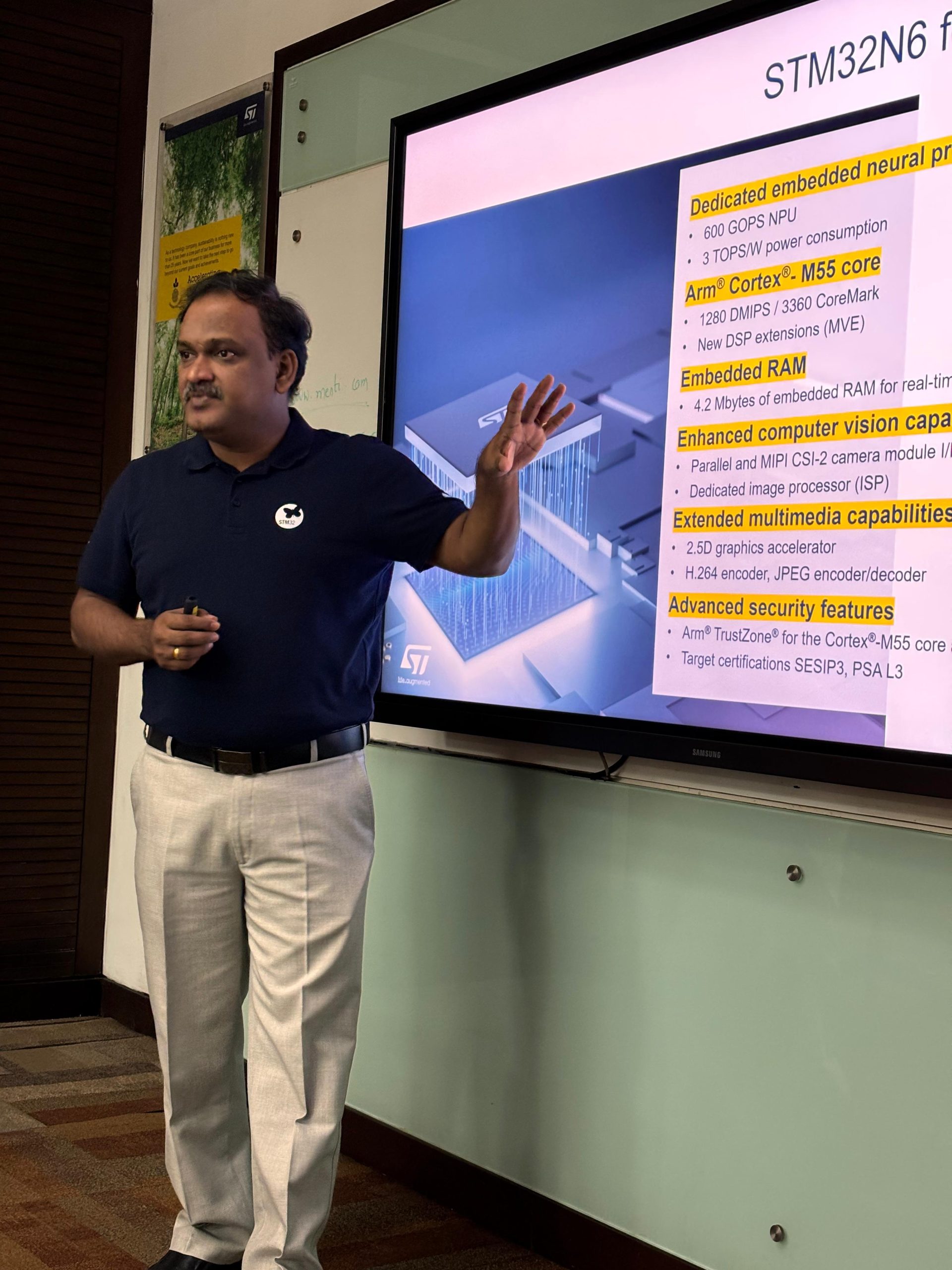
STMicroelectronics enables unmatched edge AI performance on MCU with STM32N6
In an era where artificial intelligence (AI) is rapidly transforming edge computing, STMicroelectronics is leading the charge with its groundbreaking STM32N6 series, featuring the Neural-ART Accelerator. This next-generation microcontroller delivers 600 times more AI performance than previous STM32 MCUs, redefining real-time AI processing for embedded systems.
 Sridhar Ethiraj, Technical Marketing – General Purpose MCU at STMicroelectronics India
In this exclusive interview, Rashi Bajpai from ELE Times sits down with Sridhar Ethiraj, Technical Marketing – General Purpose MCU at STMicroelectronics India, to explore the technological breakthroughs behind the STM32N6. We discuss the challenges of integrating high-performance AI with ultra-low power consumption, the real-world impact of AI-accelerated MCUs in industries like automotive, healthcare, and smart devices, and how ST’s Edge AI Suite is simplifying AI deployment for developers worldwide.
With industry giants like LG, Lenovo, and Alps Alpine already leveraging the STM32N6, this conversation unveils how AI-powered microcontrollers are shaping the future of intelligent embedded systems.
Excerpts:
STMicroelectronics has introduced the STM32N6 MCU with the Neural-ART Accelerator, delivering 600 times more machine-learning performance than previous high-end STM32 MCUs. What key challenges did ST overcome to integrate such advanced AI capabilities into a microcontroller while maintaining power efficiency?
Ans: STMicroelectronics faced several key challenges while integrating the Neural-ART Accelerator into the STM32N6 MCU. The need for high computing power for advanced AI features clashed with power efficiency goals was a major hurdle. ST tackled this by creating its own neural processing unit (NPU) to handle most AI tasks while keeping power use low. Making the system work with different AI frameworks and models also proved tough, but ST fixed this by supporting common frameworks like TensorFlow Keras, and the ONNX ecosystem. ST also had to tweak the hardware to run neural networks for computer vision and audio in real-time. This meant building a computer vision pipeline and special image processing abilities. In the end, all this work resulted in the STM32N6 MCU, which offers 600 times better machine-learning performance than earlier top-end STM32 MCUs, while still being very power-efficient.
With AI inference moving to the edge, how does the STM32N6 differentiate itself from other AI-enabled MCUs in terms of performance, memory, and AI software support?
Ans: The STM32N6 series redefines AI-enabled microcontrollers with its Neural-ART Accelerator, a custom neural processing unit (NPU) delivering up to 600 GOPS for real-time neural network inference. Built on the Arm Cortex-M55 core running at 800 MHz, it leverages Arm Helium vector processing to enhance DSP performance. With 4.2 MB of built-in RAM and high-speed external memory interfaces, it excels in AI and graphics-intensive applications. Backed by a comprehensive AI software ecosystem—including STM32Cube.AI, ST Edge AI Developer Cloud, and the STM32 model zoo—it simplifies model optimization and deployment. This seamless blend of hardware acceleration and software support makes the STM32N6 a powerful and scalable solution for edge AI workloads.
The STM32N6 has been tested and adopted by industry leaders like LG, Lenovo, and Alps Alpine. Can you share some real-world applications where this MCU is making a significant impact?
Ans: The STM32N6 MCU is driving innovation across multiple industries. In automotive, it powers advanced driver assistance systems (ADAS) by enabling real-time processing of camera and sensor inputs for collision avoidance and lane-keeping. In smart home technology, companies like LG and Lenovo use it in security cameras and smart doorbells, leveraging its AI capabilities for motion detection and facial recognition. In healthcare, it enhances medical devices by accurately processing patient data for diagnostics and continuous monitoring. These real-world applications highlight how the STM32N6 delivers high-performance AI processing, improving safety, efficiency, and user experience across industries.
AI at the edge is evolving rapidly, particularly in vision, audio processing, and sensor-based analytics. How does ST’s Edge AI Suite support developers in optimizing AI models for the STM32N6, and what industries stand to benefit the most from this innovation?
Ans: Through three main tools in the Edge AI Suite from ST, developers gain complete functionality to improve AI models for the STM32N6 platform: STM32Cube.AI and ST Edge AI Developer Cloud and STM32 model zoo. The tools in this platform optimize AI model deployment on the Neural-ART Accelerator of STM32N6 while supporting the entire process from data preparation to code generation. The STM32N6 has the potential to revolutionize multiple sectors including automotive production, automotive components and consumer electronics together with healthcare and industrial automation markets. The STM32N6 allows advanced driver assistance systems (ADAS) in automotive applications as it provides healthcare products with real-time data analysis capabilities. Through their suite developers can build effective edge AI solutions which operate throughout numerous applications.
Looking ahead, how does STMicroelectronics envision the future of AI-accelerated microcontrollers, and what role will the STM32N6 series play in shaping next-generation embedded systems?
Ans: STMicroelectronics envisions a future where AI-accelerated microcontrollers like the STM32N6 series play a pivotal role in edge computing, enabling smarter, more efficient, and autonomous embedded systems. The STM32N6, with its Neural-ART Accelerator, is designed to handle complex AI tasks such as computer vision and audio processing with exceptional efficiency. Its energy-optimized AI processing will drive advancements across automotive, healthcare, consumer electronics, and industrial automation, enabling real-time data analysis, improved user experiences, and enhanced operational efficiency. As AI at the edge continues to evolve, the STM32N6 series will be instrumental in shaping intelligent, responsive, and secure next-generation embedded systems.
Sources:
STMicroelectronics to boost AI at the edge with new NPU-accelerated STM32 microcontrollers – ST News
STM32N6 series – STMicroelectronics
STM32N6-AI – AI software ecosystem for STM32N6 with Neural-ART accelerator – STMicroelectronics
Microcontrollers-stm32n6-series-overview.pdf
The post STMicroelectronics enables unmatched edge AI performance on MCU with STM32N6 appeared first on ELE Times.
EEVblog 1673 - JBL Partybox 310 Repair - Part 2 (SPOILER)
Diy 3 channel equalizer. First audio project
 | submitted by /u/gdma2004 [link] [comments] |
EEVblog 1672 - JBL REPAIR: You'll never guess the fault!
Pages


![[link]](https://i.redd.it/g29jl5iduume1.png)