
Feed aggregator
Basic design considerations for anti-tampering circuits

Tamper detection devices, commonly built around switches and sensors, employ several techniques according to design specifications and operating environments. T. K. Hareendran examines several anti-tampering device designs to educate and inform users on various aspects of tamper detection circuits. He also presents anti-tampering use cases built around switches and sensors.
Read the full article at EDN’s sister publication, Planet Analog.
Related Content
- Prevent tampering in energy meters
- Achieve tamper-proof capacitive sensing
- What tamper detection IP brings to SoC designs
- Don’t trust your tamper detection circuitry, it may be dumb?
- Anti tamper real time clock (RTC) – make your embedded system secure
The post Basic design considerations for anti-tampering circuits appeared first on EDN.
How find track
 | Inverter pcb [link] [comments] |
Моніторинг харчових відходів у КПІ ім. Ігоря Сікорського

У відповідності до вимог законодавства України, зокрема законів України «Про якість та безпеку харчових продуктів і продовольчої сировини», «Про управління відходами», «Про охорону навколишнього природного середовища», «Про захист прав споживачів», «Про забезпечення санітарного та епідемічного бл
Synopsys Interconnect IPs Enabling Scalable Compute Clusters
Courtesy: Synopsys
Recent advancements in machine learning have resulted in improvements in artificial intelligence (AI), including image recognition, autonomous driving, and generative AI. These advances are primarily due to the ability to train large models on increasingly complex datasets, enabling better learning and generalization as well as the creation of larger models. As datasets and model sizes grow, there is a requirement for more powerful and optimized computing clusters to support the next generation of AI.
With more than 25 years of experience in delivering field-proven silicon IP solutions, we are thrilled to partner with NVIDIA and the NVIDIA NVLink ecosystem to enable and accelerate the creation of custom AI silicon. This strategic collaboration will leverage Synopsys’ expertise in silicon IPs to assist in the development of bespoke AI silicon, forming the foundation for advanced compute clusters aimed at delivering the next generation of transformative AI experiences.
Compute challenges with larger datasets and increasingly large AI modelsTraining trillion-parameter-plus models on large datasets necessitates substantial computational resources, including specialized accelerators such as Graphics Processing Units (GPUs) and Tensor Processing Units (TPUs). AI computing clusters incorporate three essential functions:
- Compute — implemented using processors and dedicated accelerators.
- Memory — implemented as High Bandwidth Memory (HBM) or Double Data Rate (DDR) with virtual memory across the cluster for memory semantics.
- Storage — implemented as Solid State Drives (SSDs) that efficiently transfer data from storage to processors and accelerators via Peripheral Component Interconnect Express (PCIe)-based Network Interface Cards (NICs).
Retimers and switches constitute the fabric that connects accelerators and processors. To enhance the computational capabilities of the cluster, it is necessary to increase capacity and bandwidth across all functions and interconnects.
Developing increasingly sophisticated, multi-trillion-parameter models requires the entire cluster to be connected over a scale-up and scale-out network so it can function as a unified computer.

Figure 1: A representative compute cluster with scale-up and scale-out network.
Standards-based IPs for truly interoperable compute clustersThe successful deployment of next-generation computing clusters relies on silicon-verified interconnects that utilize advanced process node technology and guarantee interoperability. Standardized interconnects enable an interoperable, multi-vendor implementation of a cluster.
PCIe is an established standard for processor-to-accelerator interfaces, ensuring interoperability among processors, NICs, retimers, and switches. Since 1992, the PCI-SIG has been defining Peripheral Component Interconnect (PCI) solutions, with PCIe now in its seventh generation. The extensive history and widespread deployment of PCIe ensure that IP solutions benefit from the silicon learning of previous generations. Furthermore, the entire ecosystem developing processors, retimers, switches, NICs, and SSDs possesses significant deployment experience with PCIe technology. Our complete IP solution for PCIe 7.0 is built upon our experience with more than 3,000 PCIe designs, launched in June 2024 with endorsements from ecosystem partners such as Intel, Rivos, Xconn, Microchip, Enfabrica, and Kandou.
When deploying trained models in the cloud, hyperscalers aim to continue utilizing their software on custom processors that interface with various types of accelerators. For NVIDIA AI factories, NVLink Fusion provides another method for connecting processors to GPUs.
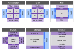
Figure 2: Components and interconnects of a next-generation compute cluster.
Accelerators can be connected in various configurations, affecting the efficiency of compute clusters. Scale-up requires memory semantics for a virtual memory pool across the cluster, while scale-out involves connecting tens-of-thousands to hundreds-of-thousands of GPUs with layers of switching and congestion management. Unlike scale-up, scale-out is more latency-tolerant and designed for bandwidth oversubscription to suit AI model data parallelism. In December 2024, we launched our Ultra Accelerator Link (UALink) and Ultra Ethernet solution to connect accelerators efficiently. The solution, which was publicly supported with quotes from AMD, Juniper and Tenstorrent, is based on silicon-proven 224G PHY and more than 2,000 Ethernet designs.
Trillion-parameter models demand extensive memory storage and high data rates for low latency access, necessitating increased memory bandwidth and total capacity. HBM provides both substantial capacity and high bandwidth. Our HBM4 IP represents the sixth generation of HBM technology, offering pin bandwidths up to 12 Gbps, which results in an overall interface bandwidth exceeding 3 TBps.
Co-packaged multi-die aggregation not only enhances compute throughput by overcoming the limitations of advanced fabrication processes but also facilitates the integration of optical interconnects through emerging Co-Packaged Optical (CPO) technologies. Since 2022, we have been developing linear electro-optical (EO) interfaces to create energy-efficient EO links. The Universal Chiplet Interconnect Express (UCIe) standard has provided a well-defined path for multi-vendor interoperability. In collaboration with Intel in 2023, we successfully demonstrated the first UCIe-connected, chiplet-based test chip.
Multi-die integration poses challenges for heat dissipation, potentially impacting temperature-sensitive photonic components or causing thermal runaway. Our comprehensive multi-die solution, including Die-to-Die IP, HBM IP, and 3DIC Compiler for system-in-package integration, provides a reliable and robust multi-die implementation.
Adopting well-established and extensively validated IP solutions across critical interconnects – from processor-accelerator interfaces to advanced multi-die architectures and HBM – mitigates the risks associated with custom design and integration. Pre-verified IPs streamline the design and verification process, accelerate timelines, and ultimately pave the way for successful first-pass silicon, enabling the rapid deployment of innovative and interoperable compute clusters.
The post Synopsys Interconnect IPs Enabling Scalable Compute Clusters appeared first on ELE Times.
Redefining Robotics: High-Precision Autonomous Mobile Robots
Courtesy: Lattice Semiconductors
Imagine a robot navigating a crowded factory floor, rerouting itself in real-time around equipment, humans, and unexpected obstacles — all while maintaining motion control and system stability. This isn’t a distant vision; this is the reality engineered by Agiliad in partnership with Lattice Semiconductor.
In a market full of autonomous mobile robots (AMRs) that rely on generic control stacks and prebuilt kits, this AMR stands out as a deep-tech system, purpose-built for intelligent indoor mobility. Unlike conventional AMRs that often trade performance for modularity or ease of deployment, this robot integrates a custom motion control framework based on Lattice’s Certus-NX FPGA, along with a ROS2-based advanced SLAM (Simultaneous Localization and Mapping), sensor fusion, and navigation stack running on NVIDIA Jetson Orin— all tightly orchestrated for low-latency, high-reliability operation.
This next-generation AMR is more than just mobile — it’s aware, adaptable, and engineered for deterministic control in real-world conditions. Designed for use in industrial settings, research labs, and beyond, the robot brings together embedded intelligence, energy efficiency, and full-stack integration to set a new benchmark for autonomous systems.
Key Features of the Robot: The Intelligence Behind the Robot
Advanced Localization & Mapping: RTAB-Map SLAM, a robust loop-closure-enabled algorithm, leverages both 3D lidar and camera feeds for consistent mapping even in environments with visual and spatial ambiguities.
- 3D Obstacle Detection & Avoidance: Using a combination of 3D voxel layers and spatio-temporal layers, the robot dynamically detects and navigates around static and moving objects — maintaining safe clearance while recalculating routes on the fly.
- Path Planning: The navigation stack uses the SMAC (Search-Based Motion Planning) planner for global routing and MPPI (Model Predictive Path Integral) for locally optimized trajectories, allowing real-time adaptation to dynamic environmental changes.
- Precision Motion Control via FPGA: BLDC motors are governed by Lattice Certus-NX FPGAs executing custom PI (proportional integral) control loops in hardware, ensuring smooth acceleration, braking, and turning — critical for safety in confined spaces.
Sensor Fusion for Environmental Awareness :
Lidar and stereo camera data is processed on the Lattice Avant-E FPGA and fused with point cloud information to detect and differentiate humans and objects, providing real-time environmental awareness for safe and adaptive navigation.

System Architecture Breakdown Diagram
The AMR’s architecture is a layered, modular system built for reliability, scalability, and low power consumption. Jetson handles ROS2 algorithms, while the Lattice FPGAs manage motion control.
- Robot Geometry and Integration with ROS2 : The robot’s geometry and joints are defined in a URDF model derived from mechanical CAD files. The Robot State Publisher node in ROS2 uses this URDF to publish robot structure and transform data across the ROS2 network.
- Lattice Avant-E FPGA Based Sensor Fusion : Sensor data from lidar and stereo vision cameras is transmitted to the Avant-E FPGA over UDP. Avant-E employs OpenCV for real-time image identification and classification, fusing visual data with point cloud information to accurately detect and differentiate humans from other objects in the environment. This fused data — including human-specific classification and distance metrics — is then transmitted to the ROS2 framework running on NVIDIA Jetson. This high-fidelity sensor fusion layer ensures enhanced situational awareness, enabling the robot to make informed navigation decisions in complex, dynamic settings.
- SLAM & Localization: Lidar provides a 3D point cloud of the environment, while the camera supplies raw image data. An RTAB-Map (Real-Time Appearance-Based Mapping) processes this information to create a 3D occupancy grid. Odometry is derived using an iterative closest point (ICP) algorithm, with loop closure performed using image data. This enables continuous optimization of the robot’s position, even in repetitive or cluttered spaces.
- Navigation: Navigation generates cost maps by inflating areas around obstacles. These cost gradients guide planners to generate low-risk paths. SMAC provides long-range planning, while MPPI evaluates multiple trajectory options and selects the safest path.
- ROS2 Control and Differential Drive Kinematics: ROS2 computes a command velocity (linear and angular) which is translated into individual wheel velocities using differential drive kinematics.
- Hardware Interface: This layer ensures integration between ROS2 and the robot’s hardware. Serial communication (UART) between Jetson and Certus-NX transmits motor velocity commands in real-time.
- Lattice Certus-NX FPGA-Based Motion Control: Lattice’s Certus-NX FPGA executes real-time motor control algorithms with high reliability and minimal latency, enabling deterministic performance, efficient power use, and improved safety under industrial loads:
PI Control Loops for velocity and torque regulation, using encoder feedback to ensure performance regardless of frictional surface conditions.
Commutation Sequencer that uses hall sensor feedback to control 3-phase BLDC motor excitation.
How It All Works Together: A Decision-Making Snapshot

The robot’s intelligence simulates a real-time decision-making loop:
Where am I?
The robot localizes using RTAB-Map SLAM with loop closure, updating its position based on visual and spatial cues.
Where should I go?
A user-defined goal (set via touchscreen or remote interface) is passed to the global planner, which calculates a safe, efficient route using SMAC.
How do I get there?
The MPPI planner simulates and evaluates dozens of trajectories in real-time, using critic-based scoring to dynamically adapt to the robot’s surroundings.
What if something blocks the path?
Sensor data updates the obstacle map, triggering real-time replanning. If no safe path is found, recovery behaviors are activated via behavior servers.
| Component / Design Element | Rationale |
| Differential Drive | Simpler control logic and reduced energy usage compared to omni-wheels |
| Lidar Placement (Center) | Avoids blind spots; improves loop closure and mapping accuracy |
| Maxon BLDC Motors | High torque (>4.5 Nm) for payload handling and smooth mobility |
| Certus-NX FPGA Motion Control | Enables deterministic control with low CPU overhead |
| Camera Integration | Improves visual SLAM and scene understanding |
| Convex Caster Wheels | Reduces ground friction, enhances turning in confined areas |
| Cooling Architecture | Fans and vents maintain safe operating temperatures |
| Jetson as CPU | Provides headroom for future GPU-based algorithm integration |
Lattice FPGA Technology
Lattice’s Certus-NX and Avant-E FPGAs deliver complementary capabilities that are critical for autonomous robotic systems:
- Low Power Consumption : Extends battery life in mobile systems
- Real-Time Performance: Delivers responsive control loops and fast data handling
- Flexible Architecture : Supports custom control logic and sensor interfaces
Combined with NVIDIA Jetson Orin and embedded vision tools, the result is a scalable and adaptable robotic platform.
Looking Ahead: Enabling the Future of Robotics
Agiliad’s engineering model emphasizes deep system-level thinking, rapid prototyping, and cross-domain integration, delivering a fully operational system within a compressed development timeline by leveraging low power Lattice FPGAs. This reflects Agiliad’s deep expertise in full-stack design and multidisciplinary integration across mechanical, electrical, embedded, and software.
The post Redefining Robotics: High-Precision Autonomous Mobile Robots appeared first on ELE Times.
The 2025 Google I/O conference: A deft AI pivot sustains the company’s relevance

The fundamental difference between Microsoft and Google’s dueling mid-May keynotes this year comes down sizzle versus steak. And that isn’t just my opinion; I can even quantify the disparity that others apparently also ascertained. As noted in my recent coverage of Microsoft’s 2025 Build conference, the full keynote ran for a minute (and a few seconds) shy of 2 hours:
But The Verge was able to condense the essentials down to a 15-minutes (and a few seconds) summary video, 1/8th the length of the original:
What about Google’s day-later alternative? It was only a couple of minutes shorter in total:
But this time, The Verge was only able to shrink it down to around 1/3 the original length, resulting in a 32-minute (and change) summary video:
Translation: nearly the same keynote duration, but much more “meat” in the Google keynote case. And that’s not even counting the 70-minute developer-tailored keynote that followed it:
That said, in fairness, I’ll point out that Google’s own summary video for the keynote was only 10 minutes long, so…
What did Google’s presenters cover in those 3+ two-keynote hours, and more generally across the two-day event (and its virtual-event precursor)? Glad you asked. In the sections that follow, I’ll touch on what I thought were at least some of the high points. For more, check out Google’s summary blogs for the developer community and the public at large, along with the conference coverage summary pages from folks like 9to5Google, Engadget, The Verge and Wired.

Conceptually similar to what Microsoft had done, Google decided to release some of its news ahead of the main event. This time, though, it was one week prior, not two. And the focus this time was on software, not hardware. Specifically, Google discussed its upcoming Expressive Design revamp of the core Android UI and associated apps, along with planned added-and-enhanced features for the O/S and apps, and related evolutions of the Android variants tailored for smart watches (Wear OS), smart glasses and headsets (Android XR), vehicles (Android Auto), displays (Google TV), and any other O/S “spins” I might have overlooked at the moment. In the process, Google got the jump on Apple, who will reportedly announce a conceptually similar revamp for its various O/Ss in a couple of weeks (stay tuned for my coverage)!
I’ll talk more about Android XR and its associated hardware, as Google did at I/O itself, in a separate topic-focused section to come later in this piece.
Multimodal large language modelsGemini, as I’ve discussed in past years’ Google I/O reports and other writeups, is the company’s suite of proprietary deep learning models, all becoming increasingly multimodal in their supported data input-and-output diversity. There are currently three primary variants:
- Pro: For coding and complex prompts
- Flash: For fast performance on complex tasks, and
- Flash-lite: For cost-efficient performance
Plus, there’s Gemma, a related set of models, this time open source, which, thanks to their comparatively low resource demands, are also useful for on-device inference with edge systems.
Latest v2.5 of Gemini Pro and Gemini Flash had both already been unveiled, but at I/O Google touted iterative updates to both of them, improving responsiveness, accuracy and other metrics. Also unveiled, this time first-time, was Gemma 3n, specifically tailored for mobile devices. And also newly announced was Gemini Live, which supports the real-time analysis and interpretation of (and response to) live audio and video feeds coming from a camera and microphone. If you’re thinking this sounds a lot like Project Astra, which I mentioned at the tail-end of last year’s Google I/O coverage (albeit not by name)…well, you’d be spot-on.
AI integration into other Google products and services…including searchJust as Microsoft is doing with its operating system and applications, Google is not only developing user direct-access capabilities to Gemini and Gemma via dedicated apps and web interfaces, it’s also embedding this core AI intelligence into its other products, such as Gmail, various Workspace apps, and Google Drive.
The most essential augmentation, of course, is that of the Google Search engine. It was Google’s first product and remains a dominant source of revenue and profit for it and parent company Alphabet, by virtue of the various forms of paid advertising it associates with search results. You may have already noticed the “AI Overview” section that for a while now has appeared at the top of search results pages, containing a summary explanation of the searched-for topic along with links to the pages used to generate that explanation:
 Well, now (as I was writing this piece, in fact!) “AI Mode” has its own tab on the results page:

And similarly, there’s now an “AI Mode” button on the Google Search home page:

Google is even testing whether to relocate that button to a position where it would completely replace the longstanding “I’m Feeling Lucky” button.
It wasn’t too long ago when various tech pundits (present company excluded, to be clear) were confidently forecasting the demise of Google’s search business at the hands of upstarts like OpenAI (more on them later). But the company’s “deft pivot” to AI teased in the title of this piece has ensured otherwise (at least until regulatory entities may say otherwise)…perhaps too much, it turns out. As I’ve increasingly used AI Overview (now AI Mode), I find that its search results summaries are often sufficient to answer my question without compelling me to click through to a content-source page, a non-action (versus tradition) that suppresses traffic to that page. Google has always “scraped” websites to assemble and prioritize search results for a given keyword or phrase, but by presenting the pages’ information itself, the company is now drawing the ire of publishers who are accusing it of content theft.
Rich content generationTake generative AI beyond LLMs (large language models) with their rudimentary input and output options (at least nowadays, seemingly…just a couple of years ago, I was more sanguine about them!), and you’re now in the realm of generating realistic still images, videos, audio (including synthesized music) and the like. This is the realm of Google’s Imagen (already at v4), Veo (now v3), and Lyria (v2 and new RealTime) models and associated products. Veo 3, for example, kicked off the 2025 Google I/O via this impressive albeit fanciful clip:
Here’s another (less silly overall therefore, I’d argue, even more impressive) one from Google:
More synthesized video examples and their associated text prompts can be found at the Veo page on the Google DeepMind site. Veo 3 is already in public release, with oft-impressive albeit sometimes disturbing results and even real-life mimickers. And combine audio, video and still images, add some additional scripting smarts, and you’ve got the new AI filmmaking tool Flow:
Who would have thought, just a few short years ago, that the next Spielberg, Scorsese, Hitchcock, Kubrick, Coppola or [insert your favorite director here] would solely leverage a keyboard and an inference processor cloud cluster as his or her content-creation toolbox? We may not be there yet, but we’re getting close…
Coding assistantsCoding is creative, too…right, programmers? Jules is Google’s new asynchronous coding agent, unveiled in Google Labs last December and now in public beta, where it goes up against
OpenAI’s recently delivered one-two punch of the internally developed Codex and acquisition (for $3B!) of Windsurf. That said, as VentureBeat also notes, it’s not even the only AI-powered coding tool in Google’s own arsenal: “Google offers Code Assist, AI Studio, Jules and Firebase”.
Android XR-based products (and partnerships)Google co-founder Sergey Brin made a curious onstage confession during a “fireside chat” session at Google I/O, admitting that he “made a lot of mistakes with Google Glass”:

His critique of himself and the company he led was predominantly two-fold in nature:
- Google tried to “go it alone” from a hardware development, manufacturing and marketing standpoint, versus partnering with an established glasses supplier such as Italian eyewear company Luxottica, with whom Meta has co-developed two generations (to date) of smart glasses (as you’ll soon learn about in more detail via an upcoming sorta-teardown by yours truly), and
- The bulbous liquid crystal on silicon (LCoS) display in front of one of the wearer’s eyes ensured that nobody would mistake them for a conventional pair of glasses…a differentiation which was not advantageous for Google.

Judging from the 2025 Google I/O messaging, the company seems determined not to make the same mistake again. It’s partnering with Warby Parker, Korea-based Gentle Monster, Samsung and Xreal (and presumably others in the future) on smart glasses based on its Android XR platform…glasses that it hopes folks will actually want to be seen wearing in public. Samsung is also Google’s lead partner for a VR headset based on Android XR…the “extended reality” (XR) that Google envisions for the operating system spans both smart glasses—with and without integrated augmented reality displays—and head-mounted displays. And it not only did live demos during the keynote but also gave attendees the chance to (briefly) try out its prototype smart glasses, glimpsed a year ago in the Project Astra clip I mentioned earlier, for themselves.
Google BeamTwo years ago, I noted that the way-cool Project Starline hologram-based virtual conferencing booth system announced two years earlier (during COVID-19 lockdowns; how apropos):
had subsequently been significantly slimmed down and otherwise simplified:
Fast forward two more years to the present and Google has rebranded the 3D-rendering technology as Beam, in preparation for its productization by partners such as HP and Zoom:
And in the process, Google has notably added near real-time, AI-powered bidirectional language translation to the mix (as well as to its baseline Google Meet videoconferencing service, which previously relied on captions), preserving each speaker’s tone and speaking style in the process:
Now there’s a practical application for AI that I can enthusiastically get behind!
OpenAI’s predictable (counter)punchIn closing, one final mention of one of Google’s primary competitors. Last year, OpenAI attempted to proactively upstage Google by announcing ChatGPT’s advanced voice mode one day ahead of Google I/O. This time, OpenAI attempted to suck the wind out of Google’s sails retroactively, by trumpeting that it was buying (for $6.5B!) the “io” hardware division of Jony Ive’s design studio, LoveFrom, one day after Google I/O. Not to mention the $3M allegedly spent on the “odd” (I‘m being charitable here) video that accompanied the announcement:
While I don’t at all discount OpenAI’s future prospects (or Meta’s, for that matter, or anyone else’s), I also don’t discount Google’s inherent advantage in developing personalized AI: it’s guided by the reality that it already knows (for better and/or worse) a lot about a lot of us.
How do you think this’ll all play out in the future? And what did you think about all the news and enhanced technologies and products that Google recently unveiled? Let me (and your fellow readers) know in the comments!
—Brian Dipert is the Editor-in-Chief of the Edge AI and Vision Alliance, and a Senior Analyst at BDTI and Editor-in-Chief of InsideDSP, the company’s online newsletter.
Related Content
- The 2024 Google I/O: It’s (pretty much) all about AI progress, if you didn’t already guess
- The 2023 Google I/O: It’s all about AI, don’t cha know
- Smart glasses skepticism: A look at their past, present, and future(?)
- Google’s fall…err…summer launch: One-upping Apple with a sizeable product tranche
The post The 2025 Google I/O conference: A deft AI pivot sustains the company’s relevance appeared first on EDN.
Made-in-India Chips Coming in 2025, Says Ashwini Vaishnaw
India is going to make their very first indigenous chip by the end of 2025, making a very important step towards technological advancements for this nation. Announcing this, Union Minister of Electronics and IT, Ashwini Vaishnaw, said that the chip employing 28-90nm technology is slated for rollout this year. This is envisaged as part of a larger plan for India to promote semiconductor manufacturing in the country and cut down on import dependency.
The first chip would be manufactured at Tata Electronics’ unit at Jagiroad in Assam, with an investment of 27,000 crore. The facility, coming up under the aegis of the India Semiconductor Mission, is a huge investment into the northeast and shall create many job opportunities. The government has also approved setting up the sixth fab in Uttar Pradesh through a JV of HCL and Foxconn, further deepening the semiconductor ecosystem in the country.
Minister Vaishnaw stated that the 28-90nm chips are used in various sectors such as automotive, telecommunications, power and railways. India, therefore, intends to focus on this segment that accounts for roughly 60 percent of the global semiconductor market so that it can position itself as a major market player.
Apart from manufacturing, the government is putting a greater emphasis on developing indigenous IP and design skills. Work is progressing towards the development of 25 chips with indigenous IP-aimed at improving cyber security. 13 projects are being pursued under the aegis of the Centre for Development of Advanced Computing (C-DAC), Bengaluru, thereby giving concrete expression to self-reliance and innovation.
Building an indigenous fab aligns with the objectives laid down in India’s “Digital India” concept, which works towards prompting India as a global nucleus for electronics manufacturing. India’s entry into the semiconductor industry is anticipated to have a significant impact on the economy both domestically and globally, given the continuous disruptions in the supply chain and in the rapidly evolving technological landscape.
Conclusion:
This initiative is directly in keeping with the “Digital India” vision to transform the country into a gobal hub for electronics manufacturing. With supply chain issues and technological shifts currently gripping the world, practically entering semiconductor production would certainly having far-reaching implications for the Indian economy as well as on the global level.
The post Made-in-India Chips Coming in 2025, Says Ashwini Vaishnaw appeared first on ELE Times.
Sumitomo Electric and Osaka Metropolitan fabricate GaN HEMT on 2-inch polycrystalline diamond
🎥 КПІшники — переможці масштабного хакатону MHP TECH Hackathon!

🏆 Команда Навчально-наукового механіко-машинобудівного інституту (НН ММІ) виборола перше місце зі 123 команд з усієї України у другому очному етапі масштабного хакатону від МХП, що проходив на території переробного комплексу в м. Ладижин (Вінницька область).
India will become the world’s electronics factory : We have the policy, the talent, and now the infrastructure to make it happen
India is making significant efforts to boost its electronics manufacturing industry with the goal of establishing itself as a prominent player in the global market. The electronics industry is witnessing remarkable growth and advancement, with a special emphasis on expanding manufacturing operations in India, particularly in the realm of semiconductor chips and electronics components. Noteworthy developments include the production of India’s first locally developed semiconductor chip in Gujarat, the initiation of state-level electronics component manufacturing programs in Tamil Nadu, and the implementation
of various PLI (Production Linked Incentive) schemes aimed at promoting local production. Furthermore, efforts are underway to establish a repairability index for electronics to tackle e-waste, and the government is actively promoting research and development as well as innovation within the sector.
India is currently enacting a series of strategic measures to enhance its electronics manufacturing sector with the aim of positioning itself as a key player on the global stage in the field of electronics production.
The “Make in India” initiative, launched to transform India into a global manufacturing hub, focuses on enhancing industrial capabilities, fostering innovation, and creating world-class infrastructure. This initiative aims to position India as a key player in the global economy by attracting investments, promoting skill development, and encouraging domestic manufacturing.
The Phased Manufacturing Programme (PMP) was introduced by the government to boost the domestic value addition in the manufacturing of mobile phones as well as their sub-assemblies and parts. The primary objective of this scheme is to stimulate high-volume production and establish a robust local manufacturing framework for mobile devices.
To enhance the growth of domestic manufacturing and foster investment in the mobile phone value chain, including electronic components and semiconductor packaging, the government introduced the Production Linked Incentive Scheme (PLI) for Large Scale Electronics Manufacturing. This initiative offers incentives ranging from 3% to 6% on incremental sales of products manufactured in India within target segments such as Mobile Phones and Specified Electronic Components.
Another initiative is the PLI scheme for passive electronic components, with a budget of INR 229.19 billion. This scheme aims to promote the domestic manufacturing of passive electronic components such as resistors and capacitors. These components are integral to various industries such as telecom, consumer electronics, automotive, and medical devices.
The Semicon India Program, initiated in 2021 with a considerable budget of ₹76,000 crore, aims to bolster the domestic semiconductor sector through a mix of incentives and strategic alliances. The comprehensive initiative not only focuses on the development of fabrication facilities (fabs) but also emphasizes on enhancing packaging, display wires, Outsourced Semiconductor Assembly and Testing (OSATs), sensors, and other vital components crucial for a thriving semiconductor ecosystem.
The Indian government is promoting research and development, along with fostering innovation, within the electronics industry. India is actively engaging in collaborations with international firms, with a specific focus on high-tech manufacturing and chip design.
India’s progress in establishing itself as a prominent destination for electronic manufacturing on the global stage has been characterized by a series of deliberate policy decisions, significant advancements in infrastructure, and a growing interconnectedness with the international community. Through careful leveraging of present circumstances and the diligent resolution of pertinent obstacles, India continues to make substantial strides towards the realization of its ambitious vision.
Devendra Kumar
Editor
The post India will become the world’s electronics factory : We have the policy, the talent, and now the infrastructure to make it happen appeared first on ELE Times.
Silicon Photonics Raises New Test Challenges
Semiconductor devices continuously experience advancements leading to technology and innovation leaps, such as we see today for applications in AI high-performance computing for data centers, edge AI devices, electrical vehicles, autonomous driving, mobile phones, and others. Recent technology innovations include Angstrom-scale semiconductor processing nodes, high-bandwidth memory, advanced 2.5D/3D heterogeneous integrated packages, chiplets, and die-to-die-interconnects to name a few. In addition, silicon photonics in a co-packaged optics (CPO) form factor promises to be a key enabling technology in the field of high-speed data communications for high-performance computing applications.
What is CPO?
CPO is a packaging innovation that integrates silicon photonics chips with data center switches or GPU computing devices onto a single substrate (see Figure 1). It addresses the growing demand for interconnects with higher bandwidth and speed, low latency, lower power consumption, and improved efficiency in data transfer for AI data center applications.

Figure 1 Co-packaged Optics (Source: Broadcom)
To understand CPO we need to first understand its constituent technologies. One such critical technology for CPO is silicon photonics. Silicon photonics provides the foundational technology for integrating high-speed optical functions directly into silicon chips. CMOS foundries have developed advanced processes based on silicon semiconductor technology to enable photonic functionality on silicon wafers. CPO uses heterogeneous integrated packaging (HIP) that integrates these silicon photonics chips directly with electronic chips, such as AI accelerator chips or a switch ASIC, on a single substrate or package. Together, silicon photonics and HIP deliver CPO products. Thus, CPO is the convergence of silicon photonics, ASICs and advanced heterogeneous packaging capability supply chains.
As mentioned earlier, CPO brings high-speed, high bandwidth, low latency, low-power photonic interconnects to the computation beachfront. In addition, photonics devices are almost loss-less for large distances enabling one such AI accelerator to share workloads with another AI accelerator hundreds of meters away, while acting as one compute resource. This high-speed and long-distance interconnect CPO fabric promises to re-architect the data center, a key innovation to unlock future AI applications.
Early CPO prototypes are being developed as of 2025 which integrate photonics “engines” with the switch or GPU ASICs on a single substrate, rather than using advanced heterogeneous packages for integration. The optical “engine” in this context refers to the packaging of the silicon photonics chips with other discrete components plus the optical fiber connector; and CPO in this context refers to the assembly of several optical engines with the switch or GPU ASICs on a common substrate.
How to Shorten CPO Time to Market?
The datacom market for CPO presents an opportunity size of about two orders of magnitude higher than what silicon photonics manufacturing supply chains have been historically accustomed to handling, such as the high-mix, low-volume products and applications in telecom and biotech. To successfully achieve CPO at this higher volume, three elements need to advance:
- The silicon photonics supply chain needs to scale up capacity and achieve high yields at wafer and at the optical engine level.
- New heterogeneous integrated packaging concepts need to be proven with the OSATs and contract manufacturers for co-packaged optics.
- New, high-volume test techniques need to be developed and proven, as the current silicon photonics testing processes are highly manual and not scalable for high volume manufacturing.
CPO technology is not mature or at high volume yet, but test equipment providers and device suppliers need to be ready for its arrival as it has a direct impact on automated test equipment test requirements, whether at the wafer, package, or system level. Investments in photonics testing capabilities are critical for developing hybrid testing systems that can keep pace with rapid advancements in photonics, and can handle both electrical and optical signals simultaneously. CPO testing requires active thermal management, high power, large package handling, custom photonic handling and alignment, high-speed digital signaling, wide-band photonic signaling, and high frequency RF signal testing.
Additionally, there are multiple test insertions from wafer to final package test that need to be optimized for test coverage, test time, and cost (see Figure 2). Expertise and experience are required to optimize the test coverage at each insertion to avoid incurring significant product manufacturing cost in both operational expense and capital equipment.

Figure 2: Silicon Photonics Wafer-to-CPO Test Insertions
CPO Test Challenges
Testing CPO devices presents unique challenges due to the diverse processes and materials involved, both electrical and photonics. A unique challenge lies in the inherent complexity of aligning optical components with the precision needed to ensure reliable test results. Optical signals are highly sensitive to minute deviations in alignment, unlike traditional electrical signals, where connection tolerances are more forgiving. The intricacies of CPO, which integrate photonics with high-digital content computing devices, demand precise positioning of lasers, waveguides, and photodetectors. Even the smallest misalignment can result in signal degradation, power loss, or inaccurate measurements, complicating test processes. As this technology advances, automated test equipment needs to evolve to accommodate the precise requirements posed by photonics and optical-electrical integration.
In addition to the precision required, the materials and processes involved in CPO introduce variability. When multiple optical chiplets from different suppliers, each using possibly different materials or designs, are packaged into a single substrate, maintaining alignment across these disparate elements becomes exponentially more difficult. Each optical chiplet may have its own unique optical properties, meaning that test equipment must handle a range of optical alignments without compromising the accuracy of signal transmission or reception. This increases the demand for automated test equipment to adapt and provide consistently reliable measurements across various types of materials and optical designs.
The time-consuming nature of achieving precise alignment also creates a significant bottleneck in high-volume semiconductor testing environments. Aligning optical components, often manually or through semi-automated processes, adds time to test cycles, which can negatively impact throughput and efficiency in production environments. To mitigate these delays, automated test equipment suppliers must invest in advanced photonics testing capabilities, such as hybrid systems that can handle both electrical and optical signals simultaneously and efficiently. These systems must also incorporate faster, more reliable alignment techniques, potentially leveraging AI-driven calibration and adaptive algorithms that can adjust in real-time.
Test meets the high-stakes needs of CPO
With the push for faster data interconnects supporting the latest industry protocols—such as PCIe 5.0/6.0/7.0 and 400G/800G/1.6T b/s Ethernet, and beyond—the stakes are high for data center reliability and performance. Any failure or suboptimal performance in data interconnects can lead to significant downtimes and performance bottlenecks. Consequently, there is a greater emphasis on enhanced test coverage to identify and address potential issues before the components are deployed in data centers. As a result, the semiconductor test industry must provide comprehensive test solutions that cover all aspects of component performance, including signal integrity, thermal behavior, and power consumption under a range of operating conditions.
Ultimately, the industry’s shift toward CPO will demand a transformation in test methodologies and equipment, with special emphasis on accurate optical alignment at all test insertions, from wafer to CPO packages. Semiconductor test leaders who invest in advanced photonics testing systems will be better positioned to handle the complexities of this emerging technology, ensuring that they can keep pace with both rapid advancements and growing market demands.
Teradyne is at the forefront of these innovations anticipating new technologies and taking a proactive approach to developing flexible and effective automated test equipment capabilities for the latest advancements in semiconductor packaging and materials.

Dr. Jeorge S. Hurtarte
Senior Director, SoC Product Strategy Semiconductor Test group
Teradyne
The post Silicon Photonics Raises New Test Challenges appeared first on ELE Times.
Enhance HMI User Experience with Built-in Large Memory MPU
Courtesy: Renesas
The HMI market continues to drive growth in better user experience and increased automation with the expansion of HMI applications. This results in a strong demand for improved functionality and performance in display-based applications, such as real-time plotting, smooth animation, and USB camera image capture, in affordable systems. Microprocessors (MPUs) with high-speed, large-capacity built-in memory that can be used like microcontrollers (MCUs) are gaining attention in the market. Renesas’ RZ/A3M MPU with a built-in 128MB DDR3L SDRAM and a compatible package for a two-layer PCB design is the ideal solution for realizing smooth animation and high-quality HMI at a reasonable system cost.
High-Performance HMI and Real-Time GraphicsIntegrating high-speed, large-capacity memory directly into the MPU package offers several advantages, including mitigating concerns about high-speed signal noise on the PCB and simplifying PCB design for the users. The large-capacity memory needed for high-performance HMIs is externally connected to the MPU in the conventional way. Additionally, PCBs equipped with DDR memory and high-speed signal interfaces require multi-layer PCB designs to account for signal noise, making it challenging to reduce PCB costs. Also, the common capacity of on-chip SRAM is typically between 1MB and 10MB, which is too small for high-performance HMIs that need to include a reasonable number of tasks in the near future. To overcome these issues, Renesas released an industry-leading RZ/A3M MPU with a large built-in 128MB DDR3L memory to support high-performance HMI and real-time graphics performance to enhance better and faster user experiences. Most importantly, the board does not require a high-speed signal interface and supports two-layer PCB design to reduce board noise and simplify system development for users.

Figure 1. Strengths of Built-in DDR Memory
Designing High-Performance PCBs at a Reasonable System CostThe number of PCB layers and the ease of design significantly impact the cost of system implementation and maintenance in user applications. As shown in Figure 2, using a wide pin pitch of 0.8mm allows for the layout of signal lines and placement of VIAs between the balls. Additionally, placing the balls handling the main signals in the outer rows of the 244-pin 17mm x 17mm LFBGA package and positioning the GND and power pins as inner balls allows for efficient routing of the necessary signal lines for the system (Figure 3). The RZ/A3M MPU is designed to build cost-effective systems with two-layer PCBs through its innovative packaging and pin assignments.

Figure 2. Signal Wiring and Ball Layout

Figure 3. Optimized Ball Arrangement for a Two-Layer Board Layout
User-Friendly Interface Enabling Smooth GUI DisplayThe high-resolution graphic LCD controller integrated into the RZ/A3M supports both parallel RGB and 4-lane MIPI-DSI interfaces, accommodating displays up to 1280×800. Additionally, the 2D graphics engine, high-speed 16-bit 1.6Gbps DDR3L memory, and 1GHz Arm Cortex-A55 CPU enable high-performance GUI displays, including smooth animations and real-time plotting that increase the possibility of automation in HMI applications. Connecting a USB camera to the USB 2.0 interface enables smooth capture of camera images, making it easy to check inside of an apparatus, for example, the doneness of the food in the oven or the condition in the refrigerator.
The EK-RZ/A3M is an evaluation kit for the RZ/A3M. It includes an LCD panel with a MIPI-DSI interface. With this kit, users can immediately start evaluation. Renesas also has several graphics ecosystem partners – LVGL, SquareLine Studio, Envox, Crank, RTOSX – who deliver GUI solutions utilizing the EK-RZ/A3M to further accelerate your development cycle.
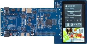
Figure 4. High-Definition HMI Example with the EK-RZ/A3M
The RZ/A3M MPU, equipped with high-speed 128MB DDR3L memory and a 1GHz Arm Cortex-A55, excels in developing cost-effective HMI applications with real-time plot UIs, smooth animations, and USB camera capture. The integrated memory simplifies PCB design by removing the need for high-speed signal interface design.
The post Enhance HMI User Experience with Built-in Large Memory MPU appeared first on ELE Times.
Zonal Architecture 101: Reducing Vehicle System Development Complexity
Courtesy: Onsemi
Thirty years ago, cars were marvels of mechanical engineering, but they were remarkably simple by today’s standards. The only electronics in an entry-level car would have been a radio and electronic ignition. The window winders were manual. The dashboard had an electromechanical speedometer and some warning lights. Power flowed directly from the battery to the headlights via a switch on the dashboard. There was no ABS, no airbags, and no centralized computer. Everything was analog and isolated.
Fast forward to today, vehicles are packed with hundreds of features, many mandated by regulation or demanded by consumers. To implement these features, automakers bolted on electronic control units (ECUs) one after another. Each system (braking, lighting, infotainment, and more) gained its own ECU, software and wiring. Over time, this created an ever-more-complex web of over 100 to 150 ECUs in a single vehicle.
To break through this complexity, automakers are embracing software-defined vehicle (SDV) architectures. SDVs aim to centralize software control, making it easier to update, manage, and extend features. But even with this shift, the underlying wiring and distributed hardware can remain a bottleneck unless automakers also rethink the vehicle’s physical architecture.
Enter zonal architecture: a modern, location-based design strategy that complements SDV principles and dramatically simplifies vehicle systems.
What Is Zonal Architecture?Zonal architecture is a paradigm shift, organizing vehicle electronics by location instead of by function. Instead of assigning each subsystem its own dedicated ECU, zone controllers are installed in each region of the vehicle, such as the front-left corner, rear-right corner, or cabin. These controllers manage local devices like lights, switches, and sensors within their respective zones. Rather than each component running its own software, the zone controller acts as a hub, handling power distribution and data communications.
These zone controllers connect to a central computer, which houses the core software that defines how the vehicle behaves. So instead of having separate ECUs for central locking, lighting, or climate control, the central compute unit makes decisions, while zone controllers carry them out.
This shift replaces hundreds of point-to-point wires with a simpler, more manageable zonal layout. By doing so, it dramatically improves design clarity and system efficiency.
Real-World Challenges of Implementing Zonal ArchitectureWhile the benefits are compelling, implementing zonal architecture isn’t without its challenges. For one, not all edge modules can be completely stripped of intelligence. Some components, such as advanced lighting systems, still require local processing for performance, safety, or proprietary functionality. Tier 1 suppliers deliver these modules with built-in software because they possess specialized knowledge of how to program and control them.
This raises a core challenge for SDVs using zonal designs: balancing centralized control with localized flexibility. In many cases, carmakers handle the central compute software, while Tier 1s manage the embedded software for the modules they manufacture. A pure, software-only central brain is a goal, but compromises are often necessary.
The Role of Ethernet in Zonal DesignsTraditional ECUs used legacy communication protocols like CAN and LIN, which were adequate for isolated modules but became unwieldy when scaled across a zonal architecture. That’s where automotive Ethernet, specifically 10BASE-T1S, comes into play.
10BASE-T1S is a low-speed (10 Mbps), multi-drop Ethernet standard designed specifically for automotive use. It enables multiple nodes (think headlights, turn signals, and door locks) to share a single twisted pair of wires, reducing the need for expensive point-to-point connections.

Figure 1. Example of 10BASE-T1S multi-drop connections
This approach simplifies cabling, lowers cost, and leverages Ethernet’s mature ecosystem, including time synchronization and error recovery, without the overhead of higher-speed Ethernet like 100BASE-T1 or gigabit Ethernet, which are unnecessary for low-bandwidth devices.
Smart Switches in Power DistributionZonal controllers not only relay data, but also distribute electrical power to the components in their zone. This means they play a critical role in system safety and diagnostics. onsemi’s smart switches go far beyond basic circuit protection. These intelligent devices offer:
- Voltage and current monitoring for each channel
- Support for automotive safety standards such as ASIL B and ASIL D
- Fail-safe and fail-operational modes, ensuring continuity of function even when faults are detected
For example, in the event of a malfunction, a smart switch can reduce power, isolate the fault, or enter a safe fallback mode rather than shutting down critical systems like headlights entirely. This level of insight and control is critical and mandatory for higher levels of automated driving.

Figure 2. Typical zonal power distribution architecture
Benefits of Zonal ArchitectureZonal architecture delivers five major advantages across vehicle development, production and operation:
- Reduced wiring harness complexity and weight: Fewer wires and connectors reduce both vehicle weight and build time.
- Lower cost of materials and assembly: Simplified wiring means reduced manufacturing cost and easier maintenance.
- Improved scalability: New features can be added or changed via software, without reengineering hardware layouts.
- Centralized software control: Streamlines development and enables over-the-air (OTA) updates, a key enabler of SDVs.
- Smarter feature coordination: Take lighting as an example. In legacy vehicles, flashing the headlights upon unlock required integrating multiple ECUs. In zonal designs, the central computer sends a single command, and the appropriate zone controller executes it—no redundant wiring or separate lighting logic required.
Zonal architecture represents a paradigm shift in how vehicles are designed and built. By grouping functions by physical location and leveraging Ethernet-based communications, automakers significantly reduce system complexity, wiring costs and maintenance challenges.
When combined with software-defined vehicle principles, zonal designs pave the way for faster innovation, greater customization, and smarter diagnostics.
With enabling technologies like 10BASE-T1S, Remote Control Protocol ICs, and intelligent power distribution, onsemi is helping carmakers bring this vision to life, delivering scalable, safe, and efficient zonal solutions that meet the evolving demands of modern mobility.
The post Zonal Architecture 101: Reducing Vehicle System Development Complexity appeared first on ELE Times.
Foxconn Taps NVIDIA to Accelerate Physical and Digital Robotics for Global Healthcare Industry
Courtesy: Nvidia
The world’s largest electronics manufacturer is building smart hospital solutions using NVIDIA technologies from the data center to the edge.
The global healthcare system is expected to face a shortage of 4.5 million nurses by 2030— and one of the main causes is high burnout. Manufacturing giant Foxconn is helping ease the burden with NVIDIA-accelerated solutions like Nurabot, a collaborative nursing robot that offloads time-consuming, fatiguing tasks such as transporting medication and samples across the hospital.
Nurabot is just one of Foxconn’s smart hospital applications developed using NVIDIA technologies and deployed by Taiwan’s leading medical centers. Its other tools include AI models to support patient health monitoring and digital twins of hospital facilities to help management teams with design and planning.
Together, these applications can transform medical centers into smart hospitals powered by NVIDIA physical AI and its three-computer solution. First, massive AI models are trained and fine-tuned on supercomputers. Next, in simulation, digital twins are used for planning, testing and robotics training — and third, edge computing systems enable rapid AI inference on robots and sensors.
Taichung Veterans General Hospital (TCVGH), Baishatun Tung Hospital – Mazu Hospital, and Cardinal Tien Hospital are among the Taiwan-based healthcare institutions adopting Foxconn’s smart hospital solutions to support clinicians and advance patient care.
“Taiwan has a highly developed healthcare infrastructure with a strong push toward digital health transformation, creating the ideal environment for robotic integration,” said Shu-Fang Liu, deputy director of the nursing department at TCVGH, which is currently conducting a field trial with Nurabot. “Robots are augmenting our capabilities so we can provide more focused, meaningful care.”
Recognized as one of the world’s top 100 smart hospitals, TCVGH is developing multiple solutions to address the severe shortage of nursing personnel in Taiwan. In addition to implementing welfare policies to retain talent, the hospital is harnessing AI technology to ease the burden on frontline staff, noted Dr. Yun-Ching Fu, the hospital’s superintendent.
The hospital began working with Foxconn last year to codevelop the Nurabot collaborative nursing robots as part of its smart healthcare initiative led by Dr. Shih-An Chen, honorary superintendent at TCVGH.
Supporting Smart Hospitals From the Data Center to the EdgeFoxconn’s smart hospital solution begins in the data center, where high-performance compute is applied to develop large AI foundation models — like FoxBrain, a large language model (LLM) developed using the NVIDIA NeMO framework. Trained on NVIDIA Hopper GPUs, FoxBrain is capable of text-to-speech, automatic speech recognition and natural language processing.
The company is also using its Honhai Super AI Computing Center 1, which features NVIDIA DGX systems, to develop healthcare-specific AI models. Offered through Foxconn’s CoDoctor AI platform, powered by NVIDIA AI, these models improve diagnostic accuracy and optimize clinical workflows for tasks including retinal imaging, vital sign monitoring, arrhythmia screening and cancer screening.

Clinicians in the radiology department at Tungs’ Taichung MetroHarbor Hospital use Foxconn’s CoDoctor AI platform for medical imaging workflows. Credit: Foxconn
Foxconn is also working with medical centers to integrate the NVIDIA AI Blueprint for video search and summarization, which can analyze real-time video data to alert healthcare workers of medical events and generate visual summaries for hospital management teams.
It will contribute CoroSegmentater, its AI model for coronary artery segmentation, to the MONAI open-source medical imaging platform pioneered by NVIDIA and leading academic medical centers. The model, powered by MONAI’s Auto3DSeg framework for 3D medical image segmentation, can be used to support diagnostics, preoperative planning and patient education.
Clinical teams can use FoxConn’s CoroSegmentater model with NVIDIA Omniverse platform to visualize the heart in 3D. Credit: Foxconn

Clinical teams can visualize these segmentations on 3D visualizations of the heart and vascular system running on NVIDIA OVX servers with NVIDIA Isaac for Healthcare, built on the NVIDIA Omniverse platform. Foxconn has also used Omniverse to develop a tool that can simulate the effects of drug treatments on the tumors of breast cancer patients.
Beyond simulating biology, Foxconn is working with TCVGH, Baishatun Tung Hospital – Mazu Hospital, and Cardinal Tien Hospital to simulate healthcare facilities using NVIDIA Omniverse. With these physically accurate simulations, the hospitals are planning out the design of new facilities, making data-driven decisions to optimize operations and building simulations to train robots.
Digital twins of TCVGH, Baishatun Tung Hospital – Mazu Hospital, and Cardinal Tien Hospital facilities. Credit: Foxconn

TCVGH, for instance, built a digital twin of one of its nursing stations and wards as a training ground for Nurabot — enabling the robotic system to practice navigating through virtual hallways before testing in the real world.
Taichung Veterans General Hospital Pilots Collaborative Nursing RobotNurabot — built by Foxconn and Japanese multinational company Kawasaki Heavy Industries — uses the FoxBrain LLM, virtual training with Isaac for Healthcare and onboard compute powered by the NVIDIA Holoscan sensor processing platform running on an NVIDIA Jetson Orin device.
Foxconn estimates that when deployed in clinical applications for delivering medication, transporting specimens and patrolling wards, Nurabot can reduce the workload of nurses by up to 30%.
“In one of our wards, we are using Nurabot to deliver wound care kits and health education materials to patient bedsides,” said Liu. “For nurses, having a robot assistant reduces physical fatigue, saving them multiple trips to supply rooms and allowing them to focus more on patients.”
TCVGH is conducting a field trial with Nurabot. Credit: TCVGH, Foxconn, Kawasaki Heavy Industries
During visiting hours, Nurabot helps guide patients and visitors through the ward, reducing the administrative workload for frontline staff. And during night shifts, where hospitals operate with fewer staff, it can help pick up the slack.
Liu hopes the nursing robots will also be able to soon converse with patients in multiple languages, recognize individuals to enable personalized interactions, and help nurses move patients.
Someone with a lung condition, for example, may need the help of two nurses to get up from their hospital bed and move to a chair to perform breathing exercises. With the help of an assistant like Nurabot, the task might be accomplished with a single nurse, allowing the other to focus on caring for the rest of the ward.
The post Foxconn Taps NVIDIA to Accelerate Physical and Digital Robotics for Global Healthcare Industry appeared first on ELE Times.
How to get great results with an infrared thermometer
Courtesy: Fluke
Temperature, Fundamentals
Infrared (IR) thermometers enable you to measure temperature quickly, at a distance, and without touching the object you’re measuring. They are so useful, easy, and even fun to use that they have become as common in kitchens as they have on factory floors. Infrared thermometers are often used to find overheated equipment and electrical circuits, but they have hundreds of other uses.

Measurement spot diameters of a Fluke 63 Infrared Thermometer at three distances.
However, there are a few “gotchas” when using an infrared thermometer that can generate readings that are misleading or just plain wrong. Fortunately, these sources of error are easy to avoid or work around.
Common uses for infrared thermometers in industry
- Finding faulty terminations in high power electrical circuits
- Locating overloaded circuit breakers
- Identifying fuses at or near their current rated capacity
- Identifying problems in electrical switch gear
- Monitoring and measuring bearing temperatures in large motors or other rotating equipment
- Identifying “hot spots” in electronic equipment
- Identifying leaks in sealed vessels
- Troubleshooting steam traps
- Finding faulty insulation in process pipes or other insulated processes
- Capturing process temperature readings
Every infrared thermometer has a “distance-to-spot” (D:S) ratio that tells you the diameter of the area being measured compared to the distance from the target. For example, if your thermometer has a distance-to-spot ratio of 12:1, it measures an approximately one-inch-diameter spot when it’s 12 inches from the target (about 2.5 cm at 30 cm). If you try to use that thermometer to measure a two-inch (5-cm) area from even just a few feet (1 m) away, you’re not going to get an accurate result because the thermometer will also be measuring the temperature outside the area you want to measure.
Distance-to-spot ratios vary a lot (from about 1:1 on the least expensive thermometers to about 60:1 on top-of-the-line models) and vary slightly with distance, so be sure to check the label on your thermometer or in the manual.
2. Lead Astray by the Laser?Most handheld infrared thermometers have laser pointers that show the approximate center of the measurement area. It’s important to know that the laser is only a pointer and not used for the actual temperature measurement. Another common misconception is that the thermometer is measuring the area illuminated by the laser beam. The measurement spot is always wider.
3. Confused by Bright Shiny Objects?Infrared thermometers have good accuracy when measuring most objects, but shiny, reflective surfaces can be a challenge. You should be especially wary when measuring the temperature of shiny metal objects, but even reflections off of glossy paint can affect accuracy. Putting a piece of non-reflective tape (such as electrical tape) over the shiny surface or applying some flat paint gives you a target from which you can get a better measurement.

Taking measurements on non-reflective tape or flat paint helps avoid errors caused by shiny surfaces.
The reason for this is that not all materials emit the same amount of infrared energy when they are at the same temperature. In general, most materials emit more infrared energy than shiny metals do – they have higher “emissivity.” (Emissivity is expressed as a number between 0 and 1, with 0 being non-emissive and 1 being perfectly emissive). Reflective surfaces are less emissive than dull surfaces. Weathered or oxidized metals are more emissive than polished, shiny metals.
If you need to take temperature readings on low emissivity objects regularly, consider an IR thermometer that enables you to compensate for variations in emissivity. For example, the Fluke 561 Infrared Thermometer enables you to set emissivity to “High” (for measuring most surfaces, such as wood, paint, rubber, plaster, or concrete), “Medium” (for oxidized metals or granite, for example), or “Low” (for shiny metals).
4. Obscured Optics?Where you use your infrared thermometer can also affect its accuracy. For example, if there is steam or dust in the between the target and the thermometer, some of the IR energy may be deflected before reaching the thermometer. Similarly, a dirty or scratched lens on your IR thermometer may impair its ability to “see” the IR energy that it needs to make a measurement. A lens that has fogged when the thermometer is brought into a warm room from a colder environment can also affect accuracy.
5. Temperature Shocked?Finally, for highest accuracy, it’s best to allow some time (about 20 minutes is usually enough) for your IR thermometer to come to the temperature of its surroundings when bringing the thermometer into surroundings that are significantly warmer or colder than where it has been stored.
Noncontact infrared thermometers offer a great combination of speed, convenience, and accuracy, but only when they’re used correctly.
To get the best results possible, remember to:- Know your IR thermometer’s distance-to-spot ratio, and get close enough to the target so your thermometer reads only the area that you want it to measure.
- Watch out for (and compensate for) shiny, “low emissivity” objects.
- Remember that steam or dust can affect the accuracy of IR thermometers.
- Keep the lens of your thermometer clean and free of scratches.
- To get the most accurate results, allow some time for the thermometer to come to the temperature of its surroundings.
The post How to get great results with an infrared thermometer appeared first on ELE Times.
Simulations à la Carte: Infusing SPICE Models for a Tasty Design Experience
Courtesy: Infineon
Have you ever noticed how the simplest dishes become unforgettable with just the right seasoning? As an Ecuadorian, I’ve learned this firsthand. A touch of “ají”—a traditional chili sauce—can transform any meal into something extraordinary. The tamarillo-based hot sauce is my personal favorite. It’s not just a condiment; it’s an experience. And when it comes to power electronics, I’ve come to see SPICE models in the same way. They’re the secret ingredient that can take your circuit simulations from bland to brilliant.
Let me show you how adding a bit of SPICE to your simulations can make all the difference.
The foundation for a flavorful design: Compact modelsThink of a compact model as your base recipe. It’s the essential framework that captures the behavior of a semiconductor device. As shown in Fig.1, a good compact model blends all the critical elements: electrical characteristics, parasitic effects, and even thermal dynamics.
For example, a compact model typically includes three layers:
– Chip model: The core of the device, accounting for its on-state and off-state characteristics, capacitances, and thermal behavior.
– Parasitic model: This layer considers resistive, inductive, and capacitive effects from the package—factors that can influence performance.
– Thermal model: It simulates how heat flows through the device, giving you insight into self-heating effects during operation.

Fig.1. A simplified structure of a compact model is shown for a SiC MOSFET in a TO247-4 package.
When these models come together, they provide a detailed picture of how a semiconductor behaves in real-world conditions. But, as with any recipe, the quality of the outcome depends on the precision and care put into each ingredient.
In the land of flavors, spicy is the king: Spice modelsIn the world of circuit simulations, SPICE models are the trusted seasoning. They’re incredibly detailed and flexible, making them perfect for analyzing switching behavior under various conditions. But just like too much chili in a dish, there’s a tradeoff: SPICE simulations can be time-consuming, especially for long-term scenarios, like a solar inverter operating over a full day.
To speed things up, designers sometimes use simplified thermal-loss models based on datasheet data. These are faster to work with but come with limitations. They often represent how a device performs on a specific test bench rather than in real-life applications, which can lead to less accurate results. A brief comparison between both abstraction levels is depicted on Fig.2.

Fig.2. Comparison of spice model and thermal-loss description models
It’s a bit like cooking with pre-made sauces—quick and convenient, but not quite as satisfying as making everything from scratch.
When life gives you chilies, make it hot: Infineon’s approachSo, how do you get the best of both worlds? How do you achieve simulations that are both fast and accurate? At Infineon, we asked these same questions, and we’ve worked hard to deliver the answers.
Our SPICE SiC MOSFET models are like your fresh, high-quality ingredients. Designed for accuracy, they provide detailed insights into dynamic response and performance. And here’s the best part: we’ve built an automated workflow that takes these models to the next level.
Using our SPICE simulator, we’ve created a system that extracts switching waveforms under various conditions, calculates energy losses, and translates them into a thermal-loss format (XML files), a simplified flow scheme is shown in the Fig. 3. This makes it easy to incorporate high-quality data into system-level simulations without sacrificing speed. Imagine having a perfectly balanced sauce ready to enhance any dish—that’s what we’re offering for your circuit designs.

Fig.3. Flow diagram to design custom thermal models using spice simulations
The finishing touchLike a great meal, a successful power converter design is all about balance. You need the right ingredients, careful preparation, and attention to detail. At Infineon, we’re passionate about helping you get it just right.
With our SPICE models and simulation tools, you’ll gain deeper insights into how our products perform in your specific applications. You’ll save time, reduce costs, and open the door to faster innovations—all while improving system performance and reliability. And let’s not forget the big win: a reduced carbon footprint, thanks to more efficient designs.
So, the next time you’re working on a simulation, remember this: a little SPICE can go a long way. Explore our tools, try our models, and see how they can transform your designs. After all, every great creation—whether it’s a dish or a circuit—deserves the perfect touch.
The post Simulations à la Carte: Infusing SPICE Models for a Tasty Design Experience appeared first on ELE Times.
Protect Your Critical Timing Applications with TimeProvider XT Extension Shelf
Courtesy: Microchip
Communications network operators who are struggling to support legacy SSU and BITS systems can now migrate to a newer platform that supports E1/T1/CC critical timing services as well as next-generation network-based timing services using PTP, NTP and Synchronous Ethernet.
The Importance of Timing ConnectionsIn today’s rapidly evolving telecommunications landscape, maintaining precise and reliable timing is crucial for the seamless operation of central office environments. Timing connections that support synchronization, timing or timestamps related to signaling information are critical. Even something as simple as NTP timing services for credit card transactions is vital.
Transitioning to Modern PlatformsNow is the time to migrate from legacy Synchronization Supply Units (SSU) and Building Integrated Timing Supply (BITS) technologies to newer platforms. These modern platforms support next-generation network-based timing services using PTP, NTP and Synchronous Ethernet as well as legacy SONET/SDH TDM synchronization.
Traditional SSU and BITS timing equipment is becoming outdated and reaching end-of-life, posing significant challenges for maintaining reliable timing services. The TimeProvider 4×00 and TimeProvider XT Extension System addresses these challenges by providing advanced timing capabilities and supporting next-generation network-based timing services. Below are several use cases outlining the value of migrating legacy synchronization to a modern platform.
Use Cases Use Case 1: Enhancing Holdover CapabilitiesIn this use case, the TimeProvider 4×00 system with dual time provider oscillators serves as the holdover oscillators for the SSU or BITS clock application. We remove the oscillators in the SSU/BITS shelf and we drive the outputs directly from the inputs. This approach is cost-effective and ensures resiliency, as many older oscillators are expensive to repair and often no longer available. The holdover hierarchy, supported by Rubidium atomic clock oscillators, meets Stratum one and G.811 requirements for synchronous Ethernet use cases. This adds holdover capability as well as next generation packet-based timing services to your offices with a very low cost and a way to ensure resiliency moving into the future. (see figure 1)
Figure 1

The Model 2 + 2 use case demonstrates the use of PTP timing services with APTS flow between two locations (e.g., central offices or mobile switching offices) A and B. This setup allows for a PTP APTS flow from location A to B and vice versa. With only one antenna per location, if a GNSS antenna fails, location A can back up location B and vice versa. By implementing this model, customers can build confidence in PTP/APTS technology and prepare for future PTP use cases. (see Figure 2)
Figure 2

The TimeProvider 4×00 and TimeProvider XT Expansion Shelf can be used to overlay legacy SSU and BITS platforms. Many of our customers have extremely old DCD or SSU and BITS platforms in place that are no longer reliable and near end of life. So, it is in the best interest of our customers to migrate the critical timing services in an office that supports signaling, transmission or high volumes of network services over to a more modern reliable platform like the Time Provider 4×00 and XT extension. (see Figure 3)
Figure 3

The final use case involves completely replacing legacy SSU BITS equipment with a TimeProvider grandmaster and XT Extension shelves that support legacy outputs. This approach is beneficial for several reasons:
- Older products are often at the end of their lifecycle.
- Customers may not need the high number of outputs provided by older platforms.
- Modern platforms consume less power, reducing overall power consumption.
- High replacement and repair costs for end-of-life SSU and BITS platforms can be avoided.
Moving to a more modern, reliable platform can actually save money in the long term related to repairs and end of life scenarios. Additionally, replacing legacy systems can help clean up office wiring issues, providing a more organized and efficient setup. (see Figure 4)
Figure 4

The good news is that it is very easy to replace a legacy office SSU/BITS with a new TimeProvider 4×00 grandmaster and XT extension. Each XT shelf has 40 individually configurable E1/T1/CC outputs, and up to five shelves can be connected, providing 200 outputs per system. This solution is backwards compatible; legacy wirewrap and patch output panels can be left in place. During a service window, simply disconnect the cable from the SSU/BITS equipment and attach it to TimeProvider XT shelf (see Figure 5).
Figure 5


Below is a simplified five-step process to replace a legacy SSU/BITS with a new TimeProvider 4×00 grandmaster and TimeProvider XT shelf fan-out.
- Install and configure the TimeProvider 4×00 grandmaster clock and XT shelve(s) in the rack near the legacy SSU/BITS.
- Install and connect the new rooftop antenna for the TimeProvider 4×00 system. Note: that the TimeProvider 4×00 system is not compatible with the legacy SSU antenna electronics.
- Confirm that the TimeProvider 4×00 system with XT shelves are fully locked to GNSS and alarm free.
- Schedule maintenance window time to disconnect output panels from the legacy BITS/SSU and reconnect them to the TimeProvider XT shelves. Or, network elements can be moved individually from the SSU/BITs equipment to the XT shelves.
- The BITS/SSU systems will switch to backup references or enter holdover with associated alarms when the legacy SSU/BITS is disconnected. Confirm that the XT shelves E1/T1/CC outputs are functioning, and all alarms have cleared.
Microchip has developed detailed procedures for exact equipment replacement scenarios. Please contact your Microchip representative for examples of detailed procedures.
TimeProvider 4×00 Grandmaster Overview and Comparison to a Legacy SSU/BITSTable 1 provides a full side by side comparison of the TimeProvider 4×00 grandmaster with XT Expansion Shelf to a legacy SSU 2000/2000e. Figure 6 is an overview of the TimeProvider XT Extension Shelf.
Table 1. Legacy SSU/BITS vs. TimeProvider 4×00 with XT extension shelf
| Functionality | DCD, SSU 2000/2000e, TP1x00, TSG-3800, TimeHub | TimeProvider 4×00 Grandmaster and XT shelf |
| Node clocks in synchronization networks ITU-T G.812 | Yes | Yes |
| Composite clock ITU G.703 | Yes | Yes |
| Input filtering of wander and jitter ITU-T G.824 | Yes | Yes |
| PRTC ITU-T G.8272 | Yes (PRTC-A and PRTC-B) | |
| ePRTC ITU-T G.8272.1 | Yes (when deployed with a collocated cesium standard ePRC clock) | |
| GNSS | GPS only | Full GNSS (GPS, Galileo, GLONASS, Beidou, QZSS, NaviC user selectable) and multi-band L1/L2/E5B/L5 support |
| BlueSky GNSS spoofing and jamming protection | Yes | |
| T1/E1/CC outputs | Yes | Yes |
| NTPr v4 and v6 with MD5 security | Yes | |
| IEEE 1588 PTP | Yes (input and output) | |
| SyncE ITU-T G.8261 | Yes |
Figure 6

The TimeProvider 4×00 and TimeProvider XT Expansion Shelf is a powerful solution for protecting and enhancing critical timing applications in central office environments. By migrating from outdated SSU and BITS technologies to modern platforms that support PTP, NTP and synchronous Ethernet, organizations can ensure the accuracy and reliability of their timing infrastructure. The use cases presented here demonstrate the versatility and benefits of the TimeProvider XT Extension Shelf, making it an essential component for any central office looking to future-proof its timing services.
Migrate your critical services timing needs to a new modern platform that can serve your existing and future requirements as you evolve your timing and network infrastructure.
The post Protect Your Critical Timing Applications with TimeProvider XT Extension Shelf appeared first on ELE Times.
Breaking the Barriers – Why Buildings Need DAS for Cellular Connectivity
Courtesy: Analog Devices
In the digital age, reliable and high-speed wireless connectivity is no longer a luxury but a necessity. From bustling urban centers to remote rural areas, the demand for seamless communication is ever-increasing. This series will delve into the world of cellular distributed antenna systems (DAS) and how integrated solutions are revolutionizing wireless coverage. This first part of the series introduces the basics of cellular DAS, its importance, and the challenges it addresses.
Enhancing Connectivity in Challenging EnvironmentsDefinition of Cellular DAS: Modern commercial buildings are marvels of engineering, but they’re also notorious for blocking cellular signals. Materials like reinforced concrete, steel, and energy-efficient glass are excellent for sustainability and safety, but they act as RF shields, severely weakening or blocking mobile signals. A cellular DAS is a network of spatially separated antenna nodes connected to a common source through fiber optic cables, which provides wireless service within a geographic area or structure. It is designed to improve cellular coverage and capacity in areas where traditional macrocell solutions are insufficient. DAS systems are particularly useful in environments with high user density, such as large buildings, stadiums, and dense urban areas.
Importance of Cellular DAS: In today’s connected world with rising expectations for always-on mobile connectivity, poor cellular signal inside buildings is no longer acceptable. Reliable wireless coverage is crucial for both personal and business communications. Cellular DAS ensures that users can maintain high-quality connections, even in challenging environments. It is essential to maintain productivity, enhance user experience, and support critical applications such as emergency services and healthcare.
Challenges Addressed by Cellular DAS: Traditional macrocell solutions often struggle with indoor coverage, capacity limitations, and interference. These challenges can lead to dropped calls, poor data speeds, and unreliable connections. Cellular DAS addresses this challenge by extending and boosting signals inside buildings. A DAS is a network of antenna nodes distributed across a facility, all connected to a central source (often through a donor antenna and head-end equipment) to ensure even, reliable cellular coverage. These nodes amplify and redistribute the incoming signal to mobile users across multiple floors or large spaces. In short, cellular DAS overcomes these challenges by providing a robust, scalable, and flexible solution that can be tailored to specific needs. Figure 1 shows a typical fully DAS architecture.
Figure 1: A Hybrid DAS Architecture
Key Components of Cellular DAS
The main components of a cellular DAS include:
- Head-End: The head-end is the central unit that connects to the base station and processes the signals. It is responsible for converting the signals from the base station into a format that the remote units can distribute.
- Transport Medium: The transport medium, such as fiber optic cables or coaxial cables, carries the signals from the head-end to the remote units. Fiber optic cables are preferred for their high bandwidth and low signal loss.
- Remote Units (Antennas): The remote units, or antennas, distribute the signals throughout the coverage area. They can be placed in strategic locations to ensure optimal coverage and capacity.
Benefits of Cellular DAS
Some of the key benefits of cellular DAS include:
- Improved Signal Strength: DAS systems can significantly improve signal strength–reducing the number of dropped calls and improving call quality.
- Enhanced Data Speeds: DAS systems can support higher data speeds by providing a more reliable and robust connection, which is essential for data-intensive applications.
- Better User Experience: Users benefit from a more consistent and reliable connection, which enhances their overall experience and satisfaction.
- Support for Multiple Carriers and Frequencies: DAS systems can support multiple carriers and frequency bands, making them highly versatile and future-proof.
Real-World Applications
Cellular DAS is widely used in various real-world applications, including:
- Large Buildings: In large office buildings, shopping malls, and other commercial spaces, DAS systems ensure reliable coverage and capacity for a large number of users.
- Stadiums and Arenas: DAS systems are essential for providing coverage to tens of thousands of spectators during events in large venues such as stadiums and arenas.
- Transportation Hubs: Airports, train stations, and other transportation hubs rely on DAS systems to ensure reliable communication for travelers and staff.
- Healthcare Facilities: Hospitals and other healthcare facilities use DAS systems to support critical communication and data transmission for patient care.
Conclusion
Understanding the fundamentals of cellular DAS is essential for grasping its significance in modern wireless networks. Cellular DAS plays a crucial role in ensuring reliable and high-speed connectivity by improving coverage and capacity. In the next part of this series, we will explore the different types of cellular DAS and their specific applications, providing a deeper understanding of how these systems can be tailored to meet various needs.
The post Breaking the Barriers – Why Buildings Need DAS for Cellular Connectivity appeared first on ELE Times.
Волонтер кафедри соціології ФСП доктор Нейтен Грінфілд: "Моя порада проста: продовжуйте вчитися!"

Вчений і дослідник у сфері теорії літератури та воєнних конфліктів, автор багатьох книжок доктор Нейтен Грінфілд живе і працює в Канаді. Другий рік поспіль він є волонтером кафедри соціології ФСП і регулярно виступає з лекціями для студентів, головно магістрантів і аспірантів. Про його академічні інтереси, "відкриття" України і досвід спілкування з українськими колегами та студентами з ним говорив професор кафедри соціології ФСП Павло Федорченко-Кутуєв.
TIL that there is no such thing as a "full bridge rectifier". It's a "bridge rectifier" or a "full wave rectifier".
Pages


![[link]](https://www.reddit.com/media?url=https%3A%2F%2Fpreview.redd.it%2Ffrmayqa3674f1.jpeg%3Fwidth%3D1024%26format%3Dpjpg%26auto%3Dwebp%26s%3D0d35287b767d0ec1f6c2c22b6224ca87cd67e45f)