
Feed aggregator
Did not have a suitable breakout board
 | submitted by /u/chanuth360 [link] [comments] |
A single op-amp solution to stabilize laser output

Semiconductor laser diodes (SLDs) are often packaged with a photodiode. The output current from this photodiode can be monitored to regulate the output power intensity of the laser diode. SLDs, however, are prone to pathological drifts, such as temperature variations and mode-hopping, that can alter the output intensity. A popular approach to stabilize the output intensity is to first convert the photodiode current to voltage. This voltage can then be read by a microcontroller, where logic can be programmed to adjust the current supplied to the laser diode. This method is illustrated in Figure 1.

Figure 1 Using a microcontroller to regulate laser diode output power by sensing photodiode current.
Wow the engineering world with your unique design: Design Ideas Submission Guide
Figure 2 provides an alternative implementation that uses a single operational amplifier. When the circuit is powered on, there is initially no photodiode current. The voltage at the positive input of the op-amp is pulled to VCC, and the op-amp powers the laser diode. This induces current in the photodiode, which creates a voltage drop across R1, setting the positive input of the op-amp to: Vcc – Iphotodiode ∗ R1.

Figure 2 A single op-amp solution using negative feedback to provide output power regulation.
The op-amp buffers this voltage and feeds it to the laser diode. The system stabilizes at an operating point determined by:
- The laser diode’s VI-intensity curve
- The coupling efficiency between the laser diode and photodiode
- The current-intensity response of the photodiode
- R1
Thereafter, negative feedback stabilizes any variations in output intensity. If the laser intensity increases, the photodiode responds by generating a higher current, which in turn creates a larger voltage drop across R1. This reduces the output voltage of the op-amp, subsequently decreasing the laser intensity. The opposite behavior is seen with a drop in laser output power.
This circuit was built on a breadboard using the OPV314 850-nm VCSEL and the OPA551P op-amp from Texas Instruments (Figure 3). R1 was set to 68 kΩ, and VCC was set to 5 V.

Figure 3 Components assembled on a breadboard using the OPV314 850-nm VCSEL and the OPA551P op-amp.
The oscilloscope trace captured from the positive node of the op-amp is shown in Figure 4, demonstrating the stable output from the laser (arbitrary units). R1 can be used to control the output power intensity.

Figure 4 Oscilloscope trace of positive node of op-amp (proxy for output laser intensity).
Anirban Chatterjee is a biomedical engineer with 10 years of experience in the consumer electronics industry. He holds a master’s degree in electrical engineering and is a member of IEEE. He holds a keen interest in biomedical sensors and associated signal processing techniques.
Related Content
- Laser Proximity Sensor Build Ideas
- LASER Diode – How it Works
- Debugging with a LASER
- Looking inside a laser measurer
The post A single op-amp solution to stabilize laser output appeared first on EDN.
Turns out fluorescent tubes make for good DIY vacuum diodes.
 | Just add a bit of epoxy and you're done. [link] [comments] |
Microchip’s PIC32A Microcontrollers Empowering the Next Generation of Embedded Systems
The embedded systems landscape is evolving rapidly in demand for AI/ML capabilities, real-time data processing and security, coasting microcontroller manufactures down a path to deliver solutions that perform high on price of power and lower cost. Hence Microchip Technology Inc. the global leader in embedded control solutions, had to rise to the challenge with its latest PIC32A series of microcontrollers.
In an exclusive interview with ELE Times, Pramit Nandy, Product Marketing Manager at Microchip’s dsPIC Business Unit, focused on motor control applications and having earned a master’s degree in electrical engineering from Arizona State University, discusses key insights into technological innovation, market strategies, and applications landscape for PIC32A MCUs.
ELE Times: What prompted the launch of the PIC32A series of MCUs? Was it based on specific market demands or technological trends?
Pramit: The launch of the PIC32A series of MCUs was prompted by specific market demands and technological trends, including the need for advanced processing capabilities for complex algorithms and data management, high-speed analog peripherals for precise measurements, robust safety and security features driven by automotive, industrial, and consumer segments, and the ability to handle software complexity with model-based designs.
ELE Times: How does the addition of 64-bit FPU enhance PIC32A MCU applications in AI/ML? Could you share any use cases or test data?
Pramit: The integration of a 64-bit Floating Point Unit (FPU) in the PIC32A MCU, operating at 200MHz, can help enhance AI/ML applications by accelerating complex mathematical operations, improving precision, enabling faster data processing, and supporting more sophisticated neural networks. Additionally, the 72-bit Multiply-Accumulate (MAC) unit in PIC32A MCUs facilitates faster algorithm processing, further boosting the capabilities required to run AI/ML-based algorithms, making it ideal for developing intelligent systems. Potential use cases include real-time data analysis, gesture recognition, predictive maintenance, and autonomous systems.
ELE Times: The PIC32A MCUs integrate a 40 Msps 12-bit ADC, a 5-nanosecond high-speed comparator and a 100 MHz GBWP operational amplifier. How do these devices work together to improve efficiency? How do you balance high-performance analog peripherals with power consumption during design time?
Pramit: The integrated 40 Msps 12-bit ADC, 5-nanosecond high-speed comparator, and 100 MHz GBWP operational amplifier in PIC32A MCUs work together to improve efficiency by enabling fast and accurate signal processing, reducing latency, and enhancing performance. The ADCs support up to 22 channels, enabling rapid and accurate data collection crucial for real-time applications. The DACs with high-speed comparators provide fast and precise signal generation, while the high-frequency op-amps ensure stable and efficient signal processing. The PIC32A family of MCUs are optimized for performance and not for low power consumption. Balancing high-performance analog peripherals with power consumption is achieved by optimizing the use of analog peripherals based on application requirements, leveraging power-saving modes, and efficient design practices.
ELE Times: How do hardware security features such as ECC, MBIST, and I/O integrity monitoring ensure the security of embedded systems? In which application scenarios are these functions particularly critical?
Pramit: Features such as ECC (Error-Correcting Code), MBIST (Memory Built-In Self-Test), and I/O integrity monitoring ensure the security of embedded systems by providing robust mechanisms to detect and correct errors, verify memory integrity, and monitor input/output operations for anomalies respectively. These functions are particularly critical in applications such as automotive systems, medical devices, and industrial control systems, where safety, security, reliability and data integrity are paramount.
ELE Times: The PIC32A MCUs are priced at less than $1 per unit, making them highly competitive in the 32-bit MCU market. How does Microchip achieve such a low cost while maintaining high performance?
Pramit: Microchip achieves low costs for PIC32A MCUs through efficient manufacturing processes, economies of scale, and optimized design that balances performance with cost-effective production.
ELE Times: How do you view the market prospects of the PIC32A MCUs in the coming years? What are Microchip’s market strategies for sectors in intelligent edge sensing, AI/ML and automotive electronics?
Pramit: The market prospects for PIC32A MCUs are promising, driven by increasing demand in intelligent edge sensing, AI/ML, and automotive electronics. Microchip’s strategies include enhancing product performance, expanding software and development tools, and forming strategic partnerships to address these growing sectors.
ELE Times: With the rapid development of IoT, AI/ML and intelligent edge computing, what new technological trends do you foresee in the MCU market, and how is Microchip responding to these trends?
Pramit: With the rapid advancement of IoT, AI/ML, and intelligent edge computing, the MCU market is experiencing new technological trends, including increased processing power, enhanced connectivity, and improved energy efficiency. In response, Microchip is developing MCUs that offer superior performance for efficiently running AI/ML algorithms, robust security features, and support for edge computing as well as IoT applications.
The post Microchip’s PIC32A Microcontrollers Empowering the Next Generation of Embedded Systems appeared first on ELE Times.
How reverse polarity protection works to safeguard car battery

Reverse polarity protection is essential in battery-connected automotive systems. So, while reverse polarity is a risky, how do we prevent it? This article delves into reverse polarity protection circuits built around standard and Schottky diodes, as well as high-side P-channel and N-channel MOSFETs. It also offers design ideas on how to implement these protection circuits efficiently.
Read the full article at EDN’s sister publication, Planet Analog.
Related Content
- How to select power line polarity protection diodes
- Protecting against reverse polarity: Methods examined, Part 1
- Protecting against reverse polarity: Methods examined, Part 2
- Protecting Against Reverse Polarity: Which Method Is Right for You?
- Schottky barrier rectifier targets power management, reverse-polarity protection applications
The post How reverse polarity protection works to safeguard car battery appeared first on EDN.
Fully automatic protective coating inspection now also on both sides and simultaneously
Expansion of the Multi Line platform with high-resolution color camera module and oblique view cameras for the inspection of protective coatings (CCI)
Protective coatings ensure the reliability of electronic assemblies. Errors in the coating can therefore have serious consequences for their function. Malfunctions or field failures cannot be tolerated, especially when used under changing climatic conditions and in safety-relevant automotive, military, avionics and telecommunications applications. Painting defects and deviations from the painting plan can now be detected automatically and reliably with the new CCI inspection system from GOEPEL electronic – for the first time simultaneously on both sides, which significantly reduces the inspection time in production.
The new Multi Line CCI for conformal coating inspection (CCI) extends the Multi Line machine platform from GOEPEL electronic. This fully automatic CCI system can inspect both from above and optionally from below. For example, dip-coated assemblies can be inspected on both sides simultaneously without having to turn the assembly over. Fully automatic return of the assemblies below the inspection level is also possible. The CCI camera module of the Multi Line CCI is equipped with a high-resolution color camera (resolution 8 µm/17 µm), telecentric optics and high-power UV LEDs for illumination from several directions with a wavelength of 365 nm. The camera module can also be equipped with four or eight angled-view cameras in order to inspect connector pins reliably from multiple viewing directions.
The upper component clearance is a comfortable 120 mm; assemblies weighing up to 15 kg can be transported. Inspection can therefore also be carried out directly in product carriers. For seamless protective coating inspection, fluorescent coatings are illuminated by the UV LEDs in the Multi Line CCI. In conjunction with the color camera, the high-resolution, telecentric optics provide high-contrast images and enable inspection within seconds.
Programming the CCI inspection is designed to be extremely user-friendly: The system is set up within a few minutes using CAD data and painting plans. Both the painted and unpainted areas of the assembly are inspected. The new system is based on the Multi Line platform with an operating system and housing optimized for professional production applications. The tried-and-tested Pilot 7.1 operating software now features the new CCI inspection function. This covers all requirements for an all-encompassing protective coating inspection and also enables the import of a painting plan. The overarching hardware and software platform character enables flexible employee scheduling and optimizes the exchange of knowledge within the company, as the AOI is operated centrally and almost identically on all Multi Line systems, without the need for extensive training.
The post Fully automatic protective coating inspection now also on both sides and simultaneously appeared first on ELE Times.
Nuvoton Launches Highly Efficient AI MCU Deployment Tool “NuML Toolkit” to Accelerate Embedded Intelligent Application Implementation
An Integrated Tool Tailored for Engineers, Enabling Fast AI Model Deployment to MCU
As AI technology rapidly integrates into various embedded systems, how to efficiently deploy trained AI models onto resource-constrained microcontrollers has become a significant challenge for engineers. To help developers quickly implement AI solutions, Nuvoton Technology has launched the NuML Toolkit. This tool integrates model conversion, project generation, deployment, and debugging processes. It is specially optimized for the NuMicro M55M1 microcontroller platform and has received widespread acclaim from users.
The NuML Toolkit offers comprehensive process support, including:
- Model Conversion and Deployment
Automatically converts Full-INT8 quantized models into .cpp files and integrates them into Arm Keil project templates.
- Toolchain Support
Supports both Keil (μVision 5 / Arm Compiler 6) and GNU Compiler Collection (make / gcc).
- High Integration
Automatically opens the Keil project and performs flashing after deployment, enabling immediate inference result viewing.
- Flexible Expandability
Developers can adjust Tensor Arena, input / output handling, and other parameters based on model needs.
- Cross-Platform Support
Uses Miniforge to set up the environment, simplifying dependency management and quickly introducing toolchains.
Three Key Advantages of NuML Toolkit:
- Fast and Simple Model Conversion
Through command-line operations, users can generate corresponding AI MCU projects with just a few parameters, without writing complex code manually.
- Integrated Workflow
From model quantization → project building → microcontroller flashing → result verification, the toolkit provides a fully integrated workflow that is easy to use for both beginners and experienced engineers.
- High Flexibility and Maintainability
The generated Keil project contains a modular code architecture (such as Application, Model, Device), making it easy for customers to modify and maintain according to actual needs. Model management is flexible—large models can be configured to use SD cards or HyperRAM, with memory usage strategies automatically adjusted based on resource allocation.
The NuML Toolkit is a highly efficient tool designed for AI applications on microcontrollers, helping customers complete AI model deployment and validation in the shortest time. It has already been widely applied in applications such as smart desk lamps, posture recognition, sound recognition, image detection, and other scenarios, becoming one of the preferred tools in the Nuvoton NuMicro AI MCU developer community.
The post Nuvoton Launches Highly Efficient AI MCU Deployment Tool “NuML Toolkit” to Accelerate Embedded Intelligent Application Implementation appeared first on ELE Times.
modified "Digital Rhythm" electronic kit
 | This is an old kid's electronics kit that I modded to a drum machine. It's based on "#106 Digital Rhythm" experiment from here: It appears to be using flip-flops to count out the beats and then play the "beeps". Main mods I did:
[link] [comments] |
Sivers provides extra details on new debt financing with US bank
Поважна делегація з Королівства Норвегії в КПІ

🇳🇴 Під час візиту до Києва поважна делегація з Королівства Норвегії на чолі з Кронпринцем Гоконом, у складі якої були Надзвичайний і Повноважний Посол Норвегії в Україні Хелене Санд Андресен і міністр енергетики Норвегії Тер'є Аасланд.
Презентація збірки поезій «Чорні тіні» Руслана Неровні

Книга діючого військового 3 ОШБр та випускника Факультета електроніки (ФЕЛ) — це форма саморефлексії, спроба осмислити власний шлях через щоденне протистояння та роздуми. Автор зізнається: «Пишеш не те, що думаєш, а те, що хочеш сказати».
Меморандум про співпрацю з Благодійним фондом Genesis for Ukraine та Благодійним фондом «КОЛО»

🤝 КПІ ім. Ігоря Сікорського підписав важливий меморандум про співпрацю з Благодійним фондом Genesis for Ukraine та Благодійним фондом «КОЛО»
The truth about Wolfspeed’s bankruptcy chatter

At a time when the explosive growth in artificial intelligence (AI), data centers, electric vehicles (EVs), and renewable energy is triggering an unprecedented demand for high-voltage, high-frequency and high-efficiency power devices, the chatter about silicon carbide (SiC) poster child Wolfspeed’s bankruptcy has startled the semiconductors world.
Wolfspeed, which divested its LED and RF businesses to focus on SiC-based power electronics, has been considered a flagbearer in the rapidly emerging SiC semiconductors market. The company pioneered 1-inch, 2-inch, 4-inch and 6-inch SiC wafers, and it was the first outfit to open an 8-inch SiC wafer fab in Mohawk Valley in 2022.
In fact, Wolfspeed is now the only company manufacturing SiC devices on 8-inch wafers in high volume. So, what has gone wrong in Wolfspeed’s SiC fairy tale? For a start, while the word bankruptcy triggers a sense of shock for a company that’s considered the market leader, the truth is that Wolfspeed is restructuring itself to address financial vows and reinforce operational efficiency.
After all, SiC is a new market that is constantly evolving. That inevitably brings growing pains, especially when a new technology like SiC entails higher product development costs while carrying small-volume orders. In other words, Wolfspeed’s situation is more than a company in crisis.

Figure 2 The SiC-based devices promise to transform power electronics in segments ranging from data centers to EVs to renewable energy. Source: Wolfspeed
Why bankruptcy
Now, let’s take a closer look at Wolfspeed’s predicament. First and foremost, a slowdown in EV demand is widely quoted as the cause of Wolfspeed’s current misfortunes. Second, while the SiC substrate business has served as the cash cow for Wolfspeed, the arrival of Chinese players has led to a steep decline in the price of SiC substrates.
According to Yole, the advent of Chinese SiC substrate suppliers has led to a significant capacity expansion and a 30% price drop in 2024. Third, and probably most important, are Wolfspeed’s financial headwinds. It’s carrying $6.5 billion debt while its sales projections seem too optimistic amid the EV slowdown and aggressive push from Chinese players in the SiC market.
So, this bankruptcy news looks more like a bid to establish supply chain discipline, capital flexibility, and policy alignment. The recent change of guards at Wolfspeed in which Gregg Lowe bowed down to make way for Robert Feurle is most likely about setting the stage for this critical transition.

Figure 2 It’s probably no coincidence that Feurle’s appointment precedes the bankruptcy news. Source: Wolfspeed
It’s pretty ironic that Wolfspeed, then known as Cree, made a huge bet on LEDs at a time when the LED market was about to crash. Nearly two decades later, Wolfspeed decided to transform itself into a power electronics device company. Yole calls it an exciting story of business transition.
While the Wolfspeed bankruptcy is most likely coming in weeks, it’s important to put things in perspective. Wolfspeed is still a market leader in SiC materials and is ranked number four in SiC power devices. That said, SiC’s technology and cost challenges leave Wolfspeed with gigantic task of turnaround in a market that demands high CapEx for future development.
Related Content
- Wolfspeed to Build 200-mm SiC Wafer Fab in Germany
- The CEO office transitions at Microchip and Wolfspeed
- Wolfspeed’s Robert Feurle Aims to Rescue Top SiC Maker
- Renesas and Wolfspeed Sign 10-Year SiC Wafer Agreement
- Wolfspeed at APEC 2025: Jay Cameron on the Growing Role of SiC
The post The truth about Wolfspeed’s bankruptcy chatter appeared first on EDN.
Power Tips # 141: Tips and tricks for achieving wide operating ranges with LLC resonant converters

Inductor-inductor-capacitor (LLC) resonant converters have a couple of appealing characteristics for applications requiring an isolated DC/DC converter such as minimal switching losses, no reverse recovery when operating below the resonant frequency and the ability to tolerate large leakage inductance within the transformer.
The challengeA primary challenge when designing an LLC converter with a wide operating range is the behavior of the gain curve with respect to equivalent load resistance. This is because as the quality factor (Qe), increases, the maximum attainable gain decreases Conversely, the minimum attainable gain increases as Qe decreases. This is shown in Figure 1 below.

![]()

Figure 1 LLC gain curves showing that, as Qe increases, the maximum attainable gain decreases. Source: Texas Instruments
This behavior makes it difficult to maintain reasonable root-mean-square (RMS) currents in the power stage and a reasonable switching frequency range. The inductance ratio (Ln) needs to be reduced to reduce the required frequency range; however, a lower inductance ratio increases the magnetizing current in the power stage. This article will discuss five tips for designing an LLC converter with a wide operating range.
Using a reconfigurable rectifierOne potential way to extend an LLC converter’s operating range is to implement a reconfigurable rectifier, as shown in Figure 2.

Figure 2 shows an LLC converter with a reconfigurable rectifier, which can be reconfigured as either a full-bridge or a voltage-doubler. Source: Texas Instruments
In this structure, you can configure the rectifier as a full-bridge or a voltage-doubler rectifier by using a comparator to look at the output voltage to decide the mode of operation. When operating as a full-bridge rectifier, Equation 3 calculates the input-to-output transfer function.
![]()
When operating as a voltage doubler rectifier, the input-to-output transfer function is:
![]()
Figure 3 shows the switching frequency versus output voltage for an LLC using the above approach to achieve a 140-V to 420-V output voltage range from a fixed 450-V input. This data is collected with an 800-mA load on the output. Notice the jump at 200 V where the comparator switches from full-bridge to voltage-doubler mode.

Figure 3 Switching frequency versus output voltage in LED driver reference design. Source: Texas Instruments
Minimizing winding and rectifier capacitanceIf the operating point drops below the minimum gain curve, the LLC controller is forced to operate in burst mode to keep the output voltage in regulation. Burst mode results in higher low-frequency output ripple voltage. This is a concern for applications requiring very low output ripple at light load and at the minimum output voltage.
In such cases, the winding capacitance within the transformer and the output capacitance (Coss) or junction capacitance (Cj) of the rectifiers must be minimized. These parasitic capacitances will cause the gain curve to invert when operating above the resonant frequency. Figure 4 shows the traditional first harmonic approximation (FHA) calculation of an LLC gain curve at light load and the same LLC gain curve when accounting for winding the capacitance and Coss of the rectifiers used in the power stage.

Figure 4 The impact of parasitic capacitance on the LLC gain curve at light load. Source: Texas Instruments
Careful attention to the winding stackup within the transformer and selection of the rectifier components minimizes this gain curve inversion effect. Using wide bandgap devices such as SIC diodes or GaN high electron mobility transistors (HEMTs) as the rectifier can result in considerably lower Coss compared to Si MOSFETs or diodes.
Using LLC controllers with a high-frequency skip modeA high-frequency skip mode can achieve a lower gain compared to what is achievable with normal switching. Below is an example from a 100-W half-bridge LLC converter with an input range of 70 V to 450 V. In Figure 5, the resonant current is shown in green, and the primary side switch node is shown in blue.
On the right side, the LLC converter is operating in a high-frequency skip mode, omitting every fourth switching cycle. The switching frequency is 260 kHz, but it is sub-modulated at a 77 kHz burst frequency.

Figure 5 The 100-W LLC converter switching behavior at 70V and 450V inputs with resonant current in green and the primary side switch node in blue. Source: Texas Instruments
Managing auxiliary bias voltagesGenerating the necessary bias voltages for the primary and secondary sides of the power supply can be done by including auxiliary windings on the LLC transformer. For LLC converters with a variable output voltage, the auxiliary winding voltages will change as the output voltage changes. This is especially true for LLC transformers using sectioned bobbins where the auxiliary windings have poor coupling to the secondary windings. When using a simple low-dropout regulator (LDO) structure to regulate the bias voltage, the efficiency will drop as the output voltage increases. It may require a larger physical package to handle the power dissipation.
In Figure 6, Naux1 and Naux2 are sized so that at the lowest output voltage, or the VCC bias voltage, is provided through D1, Q1, and D4. As the output voltage increases, the voltage on C2 is limited to the breakdown voltage of Zener D3 minus the gate-source threshold voltage of Q1. As the output voltage is increased further, the voltage generated by Naux2 becomes high enough to supply VCC, and Q1 is forced off as the gate-source voltage decreases below the turn-off threshold.

Figure 6 Using auxiliary windings along with an LDO structure to generate the necessary bias voltages for the primary and secondary side of the power supply. Source: Texas Instruments
This approach is more efficient than a single winding + LDO but requires two aux windings. An alternative approach that requires only one aux winding is to use a buck converter or boost converter instead of an LDO.
Managing trickle-charging for deeply discharged batteriesLLC converters used as battery chargers must safely recover deeply discharged batteries by applying a small charging current until the battery pack voltage is high enough to safely take the full charging current. LLCs cannot regulate down to a 0-V output with a small output current and therefore struggle to meet this requirement.
This can be managed by including a small constant current circuit with a bypass FET in parallel, as shown in Figure 7. When in trickle-charge mode, the bypass FET turns off, and the output current is supplied by LM317 configured to regulate the output current. This allows the minimum output voltage of the LLC converter to be greater than 0 V, even with an output voltage of 0 V. This approach allows the LLC transformer to generate the necessary bias voltages on the primary and secondary side and avoid needing a separate bias supply when the output voltage is 0 V. Once the battery pack voltage has risen to a high-enough level, a FET with a discrete charge-pump circuit bypasses the constant-current circuit.

Figure 7 LLC with a trickle charging circuit that can safely recover deeply discharged batteries. Source: Texas Instruments
Wide LLC operationWhile achieving a wide operating range with an LLC converter may look difficult due the nature of the LLC topology, several strategies exist for obtaining a wide operating range easier to achieve. The five simple tips and tricks listed here are analog-control friendly and do not require more complex, digital-control implementations.
 Ben Lough is a Systems Engineer in Texas Instrument’s Power Design Services team focused on power factor correction and isolated DC/DC conversion. He received his MS in Electrical and Computer Engineering from Ohio State University in 2016 and BS in ECE from Ohio State in 2015.
Related Content
- Power Tips #117: Measure your LLC resonant tank before testing at full operating conditions
- Power Tips #137: Implementing LLC current-mode control on the secondary side with a digital controller
- Power Tips #84: Think outside the LLC series resonant converter box
- Power Tips #103: LLC design considerations for audio amplifiers
The post Power Tips # 141: Tips and tricks for achieving wide operating ranges with LLC resonant converters appeared first on EDN.
Hongfa compact active suspension power design will transform driving
High-density power modules and 48V power delivery network enable midrange vehicles to adopt luxury feature
Xiamen Hongfa Electroacoustic Co., Ltd (Hongfa) has designed the industry’s highest performance and smallest active suspension power system with a goal to drive what has been a long-time luxury feature into the midrange vehicle class. Overcoming decades of false starts by prominent automotive technology providers, Hongfa struck a balance between the need to manage active suspension system size, weight and transient performance against the requirement for higher efficiency, improved EMI and symmetrical regenerative power capacity.
As an automotive power management and distribution specialist, whose relays are enabling new 48V zonal architectures, Hongfa partnered with Vicor to integrate a fixed-ratio 800V-48V DC-DC converter power module that sits alongside a network of sensors, electromechanical actuators and sophisticated software to adjust vehicle suspension in real time. The collaboration yielded the smallest active suspension system – almost half the size of the nearest competitor – with the industry’s fastest power conversion transient response.
High-voltage batteries and a 48V PDN trigger a revolution for the Hongfa active suspension vision
Whether a vehicle is on a worn highway, a backcountry dirt lane or navigating suburban potholes, active suspension provides better handling, a smoother, safer ride and reduced road noise. Early industry efforts in the 1970s included a complex electromagnetic solution which strained the capabilities of 12V battery power systems and required four 200-pound motors.
Historically, 12VDC has proven to be inadequate for powering active suspension motors without adding size, weight and cost. Additionally, some conventional DC-DC converters can deliver power without the need for an intermediate battery, but the tradeoff is that they are bulky and lack the fast transient response time required to meet the regenerative demands to recoup and store power.
Despite a history of power-hungry, heavy loads, active suspension systems stand to benefit from today’s higher voltage (400V or 800V) primary batteries and the industry’s adoption of 48V power delivery networks (PDNs); a combination is already powering plug-in hybrids and BEVs.
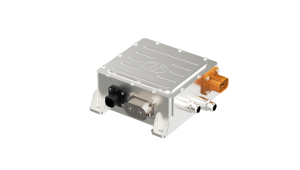 Figure — The Hongfa active suspension system (Power System Specs HF3661 800V-48V DC-DC System) is liquid cooled and is the most compact on the market, weighing 2.6kg and measuring 197 x 201 x 71mm.
Vicor fixed-ratio 800V to 48V DC-DC BCM bus converters are inherently bidirectional and provide the fastest transient response (8 million amps/second) of any DC-DC converter topology. BCMs also offer symmetrical bidirectional performance with the ability to buck or boost with the same power level. Their advanced planar packaging simplifies thermal management system design, further reducing overall footprint and weight.
Linking active suspension directly to the main battery with a bidirectional power converter enables optimal energy recuperation. Similar to how a spring absorbs and releases energy, active suspension uses regenerative shock absorbers to collect kinetic energy that is returned to the battery.
Hongfa introduces smallest active suspension system using power modules and 48V
The Hongfa solution leverages Vicor high-density power modules to create a compact (197 x 201 x 71mm) 5kW power supply for each actuator. The system can rapidly process up to 6kW of peak power in either direction. The design of the converter is greatly simplified by using a pair of Vicor BCM6135 modules operating in parallel, instead of several hundred discrete components.
The converter is optimized to work with 800V battery systems and has an operating range between 420V to 920V. With liquid cooling it can deliver up to 100A of current with 97.3% efficiency. The system housing volume is under 1.8l and weighs 2.6kg, providing a major reduction over other systems.
“When it comes to active suspension, our OEM customers require a DC-DC converter with a response rate measured in milliseconds, otherwise, additional battery support is needed,” said Peter Li, Director of Research and Development at Hongfa. “Vicor’s BCM6135 power modules not only delivered the performance we need, they also significantly shortened our development time and have made designing this system much easier for us.”
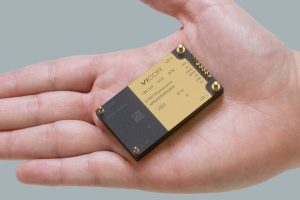 Figure — The bidirectional BCM6135 rapid current transient response rate of 8 million amps/second is a perfect match for the power profiles of active suspension and power regeneration demands. The BCM6135 is a 95% efficient 3.5kW peak power 800V-48V bus converter that can provide symmetrical power switching performance.
The combination of 48V and high-density power modules is enabling new levels of innovation in automotive electrification – reducing space, weight and providing superior performance. Together, Hongfa and Vicor are leveraging their automotive expertise to develop advanced technology and support the evolution of high-performing electric vehicles.
The post Hongfa compact active suspension power design will transform driving appeared first on ELE Times.
TI teams with NVIDIA to bring efficient power distribution to AI infrastructure
What’s new
Texas Instruments (TI) announced it is working with NVIDIA in the development of power management and sensing technologies for will help enable NVIDIA’s future 800V high-voltage direct current (HVDC) power distribution systems for data center servers. The new power architecture paves the way for more scalable and reliable next-generation AI data centers.
Why it matters
With the growth of AI, the power required per data center rack is predicted to increase from 100kW today to more than 1MW in the near future. To power a 1MW rack, today’s 48V distribution system would require almost 450lbs of copper, making it physically impossible for a 48V system to scale power delivery to support computing needs in the long term.
The new 800V high-voltage DC power-distribution architecture will provide the power density and conversion efficiency that future AI processors require, while minimizing the growth of the power supply’s size, weight and complexity. This 800V architecture will enable engineers to scale power-efficient racks as data-center demand evolves.
“A paradigm shift is happening right in front of our eyes,” said Jeffrey Morroni, director of power management research and development at Kilby Labs and a TI Fellow. “AI data centers are pushing the limits of power to previously unimaginable levels. A few years ago, we faced 48V infrastructures as the next big challenge. Today, TI’s expertise in power conversion combined with NVIDIA’s AI expertise are enabling 800V high-voltage DC architectures to support the unprecedented demand for AI computing.”
“Semiconductor power systems are an important factor in enabling high-performance AI infrastructure,” said Gabriele Gorla, VP of System Engineering of NVIDIA. ” NVIDIA is teaming with suppliers to develop an 800V high-voltage DC architecture that will efficiently support the next generation of powerful, large-scale AI data centers.”
The post TI teams with NVIDIA to bring efficient power distribution to AI infrastructure appeared first on ELE Times.
3D printed soldering jigs
 | Working on something where I am making many of these PCBs populated with 81 LEDs each. Trying to streamline as much as possible, I 3D printed a few guides/jigs to make assembling and soldering them easier. I'm a novice at 3D printing (and electronics for that matter...) but I'm enjoying having it for things like this! [link] [comments] |
I made a tiny step-down converter that fits inside a Deutsch connector
 | It's designed to step 12 or 24V down to 5V to power sensors in automotive/robotics wiring harnesses. Can do 2A continuously and 4A peak. It goes in a Deutsch connector so it can be potted in epoxy and made fully waterproof. [link] [comments] |
Thank GOD they clarified it isn't up to scale!
 | submitted by /u/Hefty-Suggestion2762 [link] [comments] |
Made this in my Electronics Class Pt. 2
 | it’s a 59 second digital clock 👍 [link] [comments] |
Pages


![[link]](https://i.redd.it/l1bko2savb3f1.jpeg)
![[link]](https://i.redd.it/2hjgphzmes2f1.png)