
Feed aggregator
CES 2026: Wi-Fi 8 silicon on the horizon with an AI touch

While Wi-Fi 7 adoption is accelerating among enterprises, Wi-Fi 8 routers and mesh systems could arrive as early as summer 2026. It’s important to note that the IEEE 802.11bn standard, widely known as Wi-Fi 8, is expected to be ratified in 2028. So, the gap between Wi-Fi 7’s launch and the potential availability of Wi-Fi 8 products in mid-2026 could shorten the typical cycle between Wi-Fi generations.
At CES 2026 in Las Vegas, Nevada, wireless chip vendors like Broadcom and MediaTek are unveiling their Wi-Fi silicon offerings. ASUS is also conducting real-world throughput tests of its Wi-Fi 8 concept routers at CES 2026.

Figure 1 Wi-Fi 8 aims to deliver a system-wide upgrade across speed, capacity, reach, and reliability. Source: Broadcom
Wi-Fi 8—aimed at boosting reliability and reducing latency in dense, interference-prone environments—marks a shift in Wi-Fi evolution. While Wi-Fi 8 maintains the same theoretical maximum data rate as Wi-Fi 7, it aims to improve effective throughput, reduce packet loss, and decrease latency for time-sensitive applications.
Another notable feature of Wi-Fi 8 designs is the incorporation of AI ingredients. Below is a short profile of an AI accelerator chip that claims to facilitate real-time agentic applications for residential consumers.
AI accelerator for Wi-Fi 8
Wi-Fi 8 proponents are quick to point out that it connects the wireless world with the AI future through highly reliable connectivity and low-latency responsiveness. Real-time, latency-sensitive applications are increasingly seeking to employ agentic AI, and for that, Wi-Fi 8 aims to prioritize consistent performance under challenging conditions.
Broadcom’s new accelerated processing unit (APU), unveiled at CES 2026, combines compute and networking ingredients with AI acceleration in a single silicon device. BCM4918—a system-on-chip (SoC) device blending compute acceleration, advanced networking, and security—aims to deliver high throughput, low latency, and intelligent optimization needed for the emerging AI-driven connected ecosystem.
The new AI accelerator for Wi-Fi 8 integrates a neural engine for on-device AI/ML inference and acceleration. It also incorporates networking engines to offload both wired and wireless data paths, enabling complete CPU bypass of all networking traffic. For built-in security, cryptographic protocol acceleration ensures end-to-end data protection without performance compromise.
“Our new BCM4918 APU, along with our full portfolio of Wi-Fi 8 chipsets, form the foundation of an AI-ready platform that not only enables immersive, intelligent user experiences but also does so with efficiency, security, and sustainability at its core,” said Mark Gonikberg, senior VP and GM of Broadcom’s Wireless and Broadband Communications Division.

Figure 2 When paired with BCM6714 and BCM6719 dual-band radios, BCM4918 APU allows designers to develop a unified compute-and-connectivity architecture. Source: Broadcom
AI compute plus connectivity
The BCM4918 APU is paired with two new dual-band Wi-Fi 8 radio devices: BCM6714 and BCM6719. While combining 2.4 GHz and 5 GHz operation into a single piece of silicon, these Wi-Fi 8 radios also feature on-chip 2.4-GHz power amplifiers, reducing external components and improving RF efficiency.
These dual-band radios, when paired with the BCM4918 APU, allow design engineers to quickly develop a unified compute-and-connectivity architecture that enables edge-AI processing, real-time optimization, and adaptive intelligence. The APU and dual-band radios for Wi-Fi 8 are now available to early access customers and partners.
Broadcom’s Gonikberg says that Wi-Fi 8 represents a turning point where broadband, connectivity, compute, and intelligence truly converge. The fact that it’s arriving ahead of schedule is a testament to its convergence merits, and that it’s more than a speed upgrade and could transform connection stability and responsiveness.
Related Content
- Broadcom delivers Wi-Fi 8 chips for AI
- Exploring the superior capabilities of Wi-Fi 7 over Wi-Fi 6
- Understanding the Differences Between Wi-Fi HaLow and Wi-Fi
- Chipsets brings Wi-Fi 7 to a broad range of wireless applications
- Europe Focuses on 6GHz Regulation, While Wi-Fi 7 Looms Beyond
The post CES 2026: Wi-Fi 8 silicon on the horizon with an AI touch appeared first on EDN.
Simple speedy single-slope ADC

Ages ago, humankind crawled out of the primordial analog ooze and began to do digital. They soon noticed and quantified a fundamental need to interconnect their new quantized numerical novelties with the classic continuum of the ancestral engineer’s world. Thus arose the ADC.
Of course, there were (and are) an abundance of ADC schemes and schematics. One of the earliest and simplest of these was the single-slope type.
Single slope ADCs come in two savory flavors. In one, a linear analog voltage ramp is generated and compared to the input signal. The time required for the ramp to rise from zero (or near) to equality with the input is proportional to the input’s amplitude and taken as its digital conversion.
We recently saw an example contributed by Dr. Jordan Dimitrov to our own friendly Design Idea (DI) corner in “Voltage-to-period converter offers high linearity and fast operation.”
In a different cultivar of the single sloper, a capacitor is charged to the input voltage, then linearly ramped down to zero. The time required to do that is proportional to Vin and counts (pun!) as the conversion result. An (extremely!) simple and cheap example of this type was published here about two and a half years ago in “A “free” ADC.”
Wow the engineering world with your unique design: Design Ideas Submission Guide
While simple and cheap are undeniably good things, too much of a good thing is sometimes not such a good thing. The circuit in Figure 1 adds a few refinements (and a bit more cost) to that basic design in pursuit of an order of magnitude (or two) better accuracy and perhaps a bit more speed.
 Figure 1 Simple speedy single-slope (SSSS) ADC biphasic conversion cycle.
Here’s how it works:
- (CONVERT = 1) switch U1 charges C1 to Vin
- (CONVERT = 0) C1 is linearly discharged by 100 µA current sourced by Z1Q1
Note: Z1, C1, and R2 should be precision types.
Conversion occurs in two phases, selected by one GPIO bit configured for output (CONVERT/ACQUIRE).
During the ACQUIRE (1) interval SPDT switch U1 connects integrator capacitor C1 to the input source, charging it to Vin. The acquisition time constant of the charging is:
C1(R sZ1+ U1 Ron, + Q2’s input impedance) = ~10 µs
To complete the charge to ½-lsb-precision at 12-bit resolution, this needs an ACQUIRE interval of:
10µs*loge(2(12+1)) = 90µs
The controlling microcontroller can then return CONVERT to zero, which switches the input side of C1 to ground, driving the base of the comparator transistor negative for a voltage step of –Vin, plus a “smidgen” (~12 mV).
This last is contributed by C2 to compensate for the zero offset that would otherwise accrue from Q2’s finite voltage gain and storage time.
Q1’s emergence from saturation drives INTEGRATE positive. Here it remains until the discharge of C1 is complete and Q1 turns back ON. This interval is:
Vin*C1 / 100µA = 200µs/v = 1-ms maximum
If the connected counter/peripheral runs at 20 MHz, then the max-count accumulation and conversion resolution will be 4000, or 11.97 bits.
This 1-ms, or ~12-bit, conversion cycle is sketched in Figure 2. Note that good integral nonlinearity (INL) and differential nonlinearity (DNL) are inherent.

Figure 2 The SSSS ADC waveshapes. The ACQUIRE duration (12 bits) is 90 µs. The INTEGRATE duration is 1ms max (Vin C1 / Iq1 = 200 µs/V). Amplitude is 5 Vpp.
Of course, not all signal sources will gracefully tolerate the loading imposed by this conversion sequence, and not all applications will find the tolerance of available LM4041 references and R1C1 adequately precise.
Figure 3 shows fixes for both of these limitations. A typical RRIO CMOS amplifier for A1 eliminates the input loading problem, and the R5 trim provides a convenient means for improving conversion calibration.

Figure 3 A1 input buffer unloads Vin, and R5 calibration trim improves accuracy.
Stephen Woodward’s relationship with EDN’s DI column goes back quite a long way. Over 100 submissions have been accepted since his first contribution back in 1974.
Related Content
- Voltage-to-period converter offers high linearity and fast operation
- A “free” ADC
- Another weird 555 ADC
- 15-bit voltage-to-time ADC for “Proper Function” anemometer linearization
The post Simple speedy single-slope ADC appeared first on EDN.
Don’t Let Your RTL Designs Get Bugged!
Courtesy: Cadence
Are you still relying solely on simulation to validate your RTL design? Is there any more validation required?
Simulation has been a cornerstone of hardware verification for decades. Its ability to generate random stimuli and validate RTL across diverse scenarios has helped engineers uncover countless issues and ensure robust designs. However, simulation is inherently scenario-driven, which means certain rare corner cases can remain undetected despite extensive testing.
This is where formal verification adds significant value. Formal doesn’t just simply mathematically analyse the entire state space of your design; it checks every possible value and transition your design could ever encounter, providing exhaustive coverage that complements simulation. No corner case is left unchecked. No bug is left hiding. Together, they form a powerful verification strategy.
Why Formal Matters in Modern Validation
Any modern validation effort needs to take advantage of formal verification, where the apps in the Jasper Formal Verification Platform analyse a mathematical model of RTL design and find corner-case design bugs without needing test vectors. This can add value across the design and validation cycle. Let’s look at some standout Jasper applications: Jasper’s Superlint and Visualise can help designers to quickly find potential issues or examine RTL behaviours without formal expertise. Jasper’s FPV (Formal Property Verification) allows formal experts to create a formal environment and sign off on the IP, delivering the highest design quality and better productivity than doing block-level simulation. Jasper’s C2RTL is used to exhaustively verify critical math functions in CPUs, GPUs, TPUs, and other AI accelerator chips.
Jasper enables thorough validation in various targeted domains, including low power, security, safety, SoC integration, and high-level synthesis verification.
“The core benefit of formal exhaustive analysis is its ability to explore all scenarios, especially ones that are hard for humans to anticipate and create tests for in simulation.”
Why Formal? Why Now?
Here’s why formal verification matters now:
- No more test vectors or random stimuli. Formally, mathematically, and automatically explores all reachable states; verification can start as soon as RTL is available without the need to create a simulation testbench.
- Powerful for exploring corner-case bugs. Exhaustive formal analysis can catch corner case bugs that escape even the most creative simulation testbenches.
- Early design bring-up made easy. Validate critical properties and interfaces before your full system is ready.
- Debugging is a breeze. When something fails, formal provides a precise counterexample, often with the shortest trace, eliminating the need for endless log hunting.
- Perfect partnership with simulation. Simulation and formal aren’t rivals; they are partners. Use simulation for broad system-level checks, and Formal for exhaustive property checking and signoff of critical blocks. Merge formal and simulation coverage for complete verification signoff.
Conclusion
As RTL designs grow in complexity and stakes rise across power, safety, and performance, relying on simulation alone is no longer enough. While simulation remains indispensable for system-level validation, formal verification fills the critical gaps by exhaustively exploring every reachable state and uncovering corner-case bugs that would otherwise slip through. By integrating formal early and throughout the design cycle, teams can accelerate bring-up, improve debug efficiency, and achieve higher confidence at signoff. In today’s silicon landscape, the most robust verification strategy isn’t about choosing between simulation and formal—it’s about combining both to ensure no bug goes unnoticed and no risk is left unchecked.
The post Don’t Let Your RTL Designs Get Bugged! appeared first on ELE Times.
Adapting Foundation IP to Exceed 2 nm Power Efficiency in Next-Gen Hyperscale Compute Engines
Courtesy: Synopsys
Competing in the booming data centre chip market often comes down to one factor: power efficiency. The less power a CPU, GPU, or AI accelerator requires to produce results, the more processing it can offer within a given power budget.
With data centres and their commensurate power needs growing exponentially, the energy consumption of each chip directly impacts the enormous costs of running gigawatt-scale AI data centres, where power and cooling account for 40–60% of operational expenditures.
To reduce the energy consumption of its workloads and gain a competitive edge, one software and cloud computing titan has made the strategic bet to design its own next-gen hyperscale System-on-Chip (SoC). By combining the advantages of new 2 nm-class process nodes with advanced, customised chip design techniques, the company is doubling down on the belief that innovation spanning process, design, and architecture can unlock new levels of power and cost efficiency.
Power play
To offer a compelling alternative in the market, the company knew that any new 2 nm design must push beyond the performance and efficiency process entitlement already baked into the scaling factors of the latest transistor fabrication methods. The transition to the 2 nm process is expected to provide 25–30% power reduction relative to the previous 3 nm node.
The company set an ambitious goal of achieving an additional 5% improvement on the 2 nm baseline. Through close collaboration with Synopsys — combining EDA software flow enhancements with our optimised Foundation IP logic library — the company exceeded its goal, achieving:
- 34% reduced power consumption with the same baseline flow.
- 51% reduced power consumption with an optimised flow.
- 5% silicon area advantage over baseline with ISO performance.
The company also evaluated our 2 nm embedded memories, which exceeded SRAM scaling expectations compared to our 3 nm product. On average, the 2 nm memory instances delivered 12% higher speed, occupied 8% less area, and consumed 12% less power than their 3 nm counterparts.
Expert collaboration
Because the transition to 2 nm comes with a shift from FinFET to GAA architecture, the company’s SoC developers faced a particularly steep learning curve, with an increase in complexity and technology assimilation.
They engaged our team in the early stages of the project — the byproduct of a trusted working relationship that spans more than four generations of AI chip designs — and even licensed our Foundation IP before the availability of any silicon reports.
The company used our IP, reference methodology, and Fusion Compiler tool to explore all commercially available options for achieving their power budget requirements. While the early development cycles produced the silicon area advantage, they did not achieve the power scaling targets the company sought.
Adaptation and optimisation
Seeking additional assistance, the company inquired whether our EDA tools and IP could be leveraged to push the design’s performance further.
R&D experts from our IP and EDA groups began collaborating on the design. Starting with the standard logic libraries, the IP group worked closely with the company’s designers to adapt and optimise the libraries with new cells and updated modelling. Over several iterations, the teams delivered the 7.34% power benefit, with Synopsys PrimePower used for final power analysis.
Our Technology and Product Development Group then helped the company take it a step further. By developing new algorithms for Fusion Compiler, and after many trials based on the latest recommended power recipe, design flow optimisations produced a 9.51% combined power benefit.
At the same time, our application engineers worked closely with the company to provide the best solution from our broad portfolio of memory compilers. Weighing performance requirements with power and area targets, we were able to extend the benefit of 2 nm beyond instance-level scaling. In one key scenario, power was reduced by an additional 25% by using an alternative configuration that met the 2 nm requirements.
Conclusion
As hyperscale compute continues its relentless push toward higher performance within ever-tighter power envelopes, success at advanced nodes like 2 nm will hinge on more than process scaling alone. This collaboration demonstrates how tightly integrated innovation across Foundation IP, EDA flows, and design methodology can unlock efficiency gains well beyond baseline node benefits. By adapting standard libraries, optimising tool algorithms, and co-engineering memory configurations, the company not only surpassed its power-efficiency targets but also achieved meaningful area and performance advantages. The outcome underscores a broader industry lesson: at 2 nm and beyond, early engagement, deep expertise, and holistic optimisation across the silicon stack will be critical to building the next generation of power-efficient hyperscale compute engines.
The post Adapting Foundation IP to Exceed 2 nm Power Efficiency in Next-Gen Hyperscale Compute Engines appeared first on ELE Times.
Delta Electronics to Provide 110 MW to Prostarm Info Systems for Energy Storage Projects in India
“At Prostarm, we are committed to bringing advanced energy solutions that empower utilities and drive India’s clean energy transition. Partnering with Delta Electronics India for the AEML’s BESS project reflects our shared vision of delivering technology-led reliability and performance at scale. This collaboration not only strengthens our portfolio in energy storage but also sets a benchmark for strategic partnerships in India’s evolving power sector.”
The post Delta Electronics to Provide 110 MW to Prostarm Info Systems for Energy Storage Projects in India appeared first on ELE Times.
TI’s vast automotive portfolio: Shift towards autonomous vehicles
Texas Instruments (TI) has introduced new automotive semiconductors and development resources to enhance safety and autonomy across vehicle models. TI’s scalable TDA5 high-performance computing system-on-a-chip (SoC) family offers power- and safety-optimised processing and edge artificial intelligence (AI) that supports up to Society of Automotive Engineers Level 3 vehicle autonomy. TI also unveiled the AWR2188, a single-chip, eight-by-eight 4D imaging radar transceiver, to help engineers simplify high-resolution radar systems. These devices, alongside the DP83TD555J-Q1 10BASE-T1S Ethernet physical layer (PHY), join TI’s broader automotive portfolio for next-generation advanced driver assistance systems (ADAS) and software-defined vehicles (SDVs). TI will be debuting these products at CES 2026, Jan. 6-9, in Las Vegas, Nevada.
“The automotive industry is moving toward a future where driving doesn’t require hands on the wheel,” said Mark Ng, director of automotive systems at TI. “Semiconductors are at the heart of bringing this vision of safer, smarter and more autonomous driving experiences to every vehicle. From detection and communication to decision-making, engineers can use TI’s end-to-end system offering to innovate what’s next in automotive.”
High-performance compute SoCs enable safe, scalable AI across vehicle models
To enhance safety and autonomy in next-generation vehicles, automakers are adopting central computing systems that support AI and sensor fusion for real-time decision-making. Designed for high-performance computing, TI’s TDA5 SoC family offers edge AI acceleration from 10 trillion operations per second (TOPS) to 1200 TOPS with power efficiency beyond 24 TOPS/W. This scalability, enabled by their chiplet-ready design with Universal Chiplet Interconnect Express interface technology, allows designers to implement different feature sets and support up to Level 3 autonomous driving using a single portfolio. Building on over two decades of experience in automotive processing, the family expands the performance of TI’s existing portfolio to enable automakers to centralise their computing architectures and process advanced AI models.
By integrating the latest generation of TI’s C7 neural processing unit (NPU), TDA5 SoCs provide up to 12 times the AI computing of previous generations with similar power consumption, eliminating the need for costly thermal solutions. This performance supports billions of parameters within language models and transformer networks, increasing in-vehicle intelligence while maintaining cross-domain functionality. The family features the latest Arm Cortex-A720AE cores, allowing automakers to integrate more safety, security and computing applications.
TDA5 SoCs reduce system complexity and costs by supporting cross-domain fusion of ADAS, in-vehicle infotainment and gateway systems within a single chip. Their safety-first architecture further simplifies systems by helping automakers meet Automotive Safety Integrity Level D safety standards without external components.
To simplify complex vehicle software management, TI is partnering with Synopsys to provide a Virtualiser development kit for TDA5 SoCs. The kit’s digital twin capabilities help engineers accelerate time-to-market for their SDVs by up to 12 months.
Single-chip, eight-by-eight radar transceiver achieves earlier, more accurate detection
With enhanced perception and reliability in any weather condition, radar is a fundamental technology for sophisticated ADAS and greater vehicle autonomy. Designed to meet global market needs, TI’s AWR2188 4D imaging radar transceiver integrates eight transmitters and eight receivers into a single launch-on-package chip. This integration simplifies higher-resolution radar systems because eight-by-eight configurations do not require cascading, while scaling up to higher channel counts requires fewer devices. The transceiver supports both satellite and edge architectures, offering automakers the flexibility to simplify and accelerate the global deployment of ADAS features across entry-level to premium vehicles.
The AWR2188 features enhanced analogue-to-digital converter data processing and a radar chirp signal slope engine, both supporting 30% faster performance than currently available solutions. This level of performance powers advanced radar use cases such as detecting lost cargo, distinguishing between closely positioned vehicles and identifying objects in high-dynamic-range scenarios. The transceiver can detect objects with greater accuracy at distances >350m, altogether enabling safer, more autonomous driving.
10BASE-T1S technology extends Ethernet to vehicle edge nodes
The acceleration toward SDVs and higher levels of autonomy is prompting a fundamental shift in subsystem architectures. Ethernet is an important enabler for this evolution, as it allows systems to collect and transmit more data across vehicle zones in real time through a simple, unified network architecture. TI’s new DP83TD555J-Q1 10BASE-T1S Ethernet Serial Peripheral Interface PHY with an integrated media access controller offers nanosecond time synchronisation, industry-leading reliability and Power over Data Line capabilities. These features enable engineers to extend high-performance Ethernet to vehicle edge nodes while reducing cable design complexity and costs.
With TI’s end-to-end system offering, which includes technologies for advanced sensing, reliable in-vehicle networking and efficient AI processing, automakers can develop systems that improve safety and automation levels across different vehicle models.
TI at CES 2026
In the Las Vegas Convention Centre North Hall, meeting room No. N115, TI will showcase how innovation across its analogue and embedded processing portfolios is reshaping what’s next in how people move, live and work. Demonstrations include advancements in vehicle technology and advanced mobility, smart homes and digital health, energy infrastructure, robotics, and data centres. See ti.com/CES.
Package, availability and pricing
- The TDA54 software development kit is now available on TI.com to help engineers get started with the TDA54 Virtualiser development kit. Samples of the TDA54-Q1 SoC, the first device in the family, will be sampled to select automotive customers by the end of 2026.
- Preproduction quantities of the AWR2188 transceiver and an evaluation module are now available upon request at TI.com.
- Preproduction quantities of the DP83TD555J-Q1 10BASE-T1S Ethernet PHY and an evaluation module are now available upon request at TI.com.
The post TI’s vast automotive portfolio: Shift towards autonomous vehicles appeared first on ELE Times.
Made a dual rail transformer using binoucular core.
 | Not sure if this is a normal way to use these cores as i have no knowledge about it. But i came up with a way to get 2 isolated outputs from 1 input. The input windings go in the middle so from hole to hole and the 2 other windings are on the sides. This specific core gave 5.4v on output with 5v input but it was just put together with scraps to see if it works and it did really well. [link] [comments] |
Mission Microwave to design and deliver solid-state power block upconverters for Telesat Lightspeed
Amazon’s Smart Plug: Getting inside requires more than just a tug

Amazon wisely doesn’t want naïve consumers poking around inside its high-voltage AC-switching devices. This engineer was also thwarted in his exploratory efforts…initially, at least.
Early last month, within a post detailing my forced-by-phaseout transition from Belkin’s Wemo smart plugs to TP-Link’s Kasa and Tapo devices, I mentioned that I’d originally considered a different successor:
Amazon was the first name that came to mind, but although its branded Smart Plug is highly rated, it’s only controllable via Alexa. I was looking for an ecosystem that, like Wemo, could be broadly managed, not only by the hardware supplier’s own app and cloud services but also by other smart home standards…

Even though I ended up going elsewhere, I still had a model #HD34BX Amazon Smart Plug sitting on my shelf. I’d bought it back in late November 2020 on sale for $4.99, 80% off the usual $24.99 price (and in response to, I’m guessing, per the purchase date, a Black Friday promotion). Regular readers already know what comes next: it’s teardown time!
Let’s start with some outer box shots, as usual (as with subsequent images), accompanied by a 0.75″ (19.1 mm) diameter U.S. penny for size comparison purposes:


Note that, per my prior writeup’s “specific hardware requirement that needed to be addressed,” it supports (or at least claims to) up to 15A of current:
- Input: 100-120V, 60 Hz, 15A Max
- Output:
- 120V, 60 Hz, 15A, resistive load
- 120V, 60 Hz, 10A, inductive load
- 120V, 60 Hz, 1/2 HP, motor load
- 120V, 60 Hz, TV-5, incandescent
- Operating Temperature: 0-35°C
- IP Rating: IP30
thereby being capable of power-controlling not only low-wattage lamps but also coffee makers, curling irons, and the like:


See that translucent strip of tape at the upper right?

Wave buh-bye to it; it’s time to look inside:


Nifty cardboard-based device-retention mechanism left over at the bottom:

The bottom left literature snippet is the usual warranty, regulatory and other gobbledygook:

The one at right is a wisp of a quick-start guide:


But neither of them, trust me I already realize, is the fundamental motivation for why you’re here today. Instead, it’s our dissection subject (why was I having flashbacks to the recently viewed and greatly enjoyed 2025 version of Frankenstein as I wrote those prior words?):


Underneath the hole at far left is an activity-and-status LED. And rotating the smart plug 90°:

there’s the companion switch, which not only allows for manual power control of whatever’s plugged into it but also initiates a factory reset when pressed and held for an extended period.
Around back are specs-and-such, including the always-insightful FCC ID (2ALBG-2017), along with the line (“hot”) and neutral source blades and ground pin (Type B NEMA 5-15 in this case):

In contrast to its left-side sibling, the right side is comparatively bland (i.e., to clarify, there’s nothing under the penny):

as are the bottom:

and the top, for that matter, unless you’re into faintly embossed Amazon logos:

My first (few…seeming few dozen…) attempts to get inside via the visible seam around the backside edges, trying out various implements of destruction in the process, were for naught:

Though the efforts weren’t completely wasted, as they motivated me to finally break out the Dremel set that had been sitting around unused and collecting dust since…yikes…mid-2005, my Amazon order history just informed me:

and which delivered ugly but effective results (albeit leaving the smart plug headed for nowhere but the landfill afterwards):


First step: unscrew and disconnect the wire going from the front panel socket’s load (“hot”) slot to the PCB (where it’s soldered):


Like I said before…ugly but effective:

At the top (in this photo, to the left when originally assembled) are the light pipe that routes the LED (yet to be seen but presumably on the PCB) output to the front panel, along with the mechanical assembly for the left-side switch:

You’ve already seen one top view of the insides, three photos ago. Here’s another, this time standalone and rotated:

And here are four of the five other perspectives; the back view will come later. Front:

Left side, showing the PCB-mounted portion of the switch assembly:

Right behind the switch is the outward-pointing LED whose location I’d just prognosticated:

Right side:

And bottom:

Onward. The ground pin from the back panel routes directly to the front panel socket’s ground slot, not interacting with any intermediary circuitry en route:


You’ve probably already noticed that the “PCB” is actually a three-PCB assembly: smaller ones at top and bottom, both 90°-connected to the main one at the back. To detach the latter from the back chassis panel requires removal of another screw:


Houston, we have liftoff:

This is interesting, at least to me. The neutral wire is attached to its corresponding back-panel blade with a screw, albeit also to the PCB at other end with solder:


but the line (“hot”) wire is soldered at both ends:

This seemingly inconsistent approach likely makes complete sense to those of you more versed in power electronics than me; please share your thoughts in the comments. For now…snip:


Assuming, per my earlier comments, that you’ve already noticed the three-PCB assembly, you might have also noticed some white tape on both sides of the mini-PCB located at the bottom. Wondering what’s underneath it? Me too:


The answer: not much of anything!
What’s the frequency, Kenneth?(At least) one more mystery to go. We’ve already seen plenty of predictable AC switching and AC-to-DC conversion circuitry, but where’s all the digital and RF stuff that controls the AC switching, along with wirelessly communicating with the outside world? For the answer, I’ll direct your attention to the mini-PCB at the top, which you may recall initially glimpsing earlier:

What you’re looking at on the other side is the WCBN4520R, a Wi-Fi-plus-Bluetooth Low Energy module discussed in-depth in an informative Home Assistant forum thread I found.

Forum participants had identified the PCB containing the module as the WN4520L from LITE-ON Technology, with Realtek’s RTL8821CSH single-chip wireless controller and Rockchip Electronics’ RKNanoD dual Arm Cortex-M3 microcontroller supposedly inside the module. But a different teardown I found right before finalizing this piece instead shows MediaTek’s MT7697N:
A highly integrated single chip offering an application processor, low power 1T1R 802.11 b/g/n Wi‑Fi, Bluetooth subsystem and power management unit. The application processor subsystem contains an ARM Cortex‑M4 with floating point unit. It also supports a range of interfaces including UART, I2C, SPI, I2S, PWM, IrDA, and auxiliary ADC. Plus, it includes embedded SRAM/ROM.
as the main IC inside the module, accompanied by a Macronix 25L3233F (PDF) 32 Mbit serial flash memory. I’m going with the latter chip inventory take. Regardless, to the left of the module is a visible silhouette of the PCB-embedded antenna, and there’s also a SMA connector on the board for tethering to an optional external antenna, not used in this particular design.

And there you have it! As always, sound off with your thoughts in the comments, please!
—Brian Dipert is the Principal at Sierra Media and a former technical editor at EDN Magazine, where he still regularly contributes as a freelancer.
Related Content
- Teardown: Smart plug adds energy consumption monitoring
- This smart plug automatically resets your router when your Internet goes out
- Limping Into the 21st Century with Smart Technology
- Teardown: A Wi-Fi smart plug for home automation
The post Amazon’s Smart Plug: Getting inside requires more than just a tug appeared first on EDN.
EDA Tools for Robust RFICs and Mixed-Signal ICs
Courtesy: Keysight Technologies
In radio frequency integrated circuits (RFICs), the high-frequency signals create unique phenomena that are not typically observed in regular digital and low-frequency analogue ICs. Even seemingly trivial design changes to an RFIC can degrade its behaviour and overall performance. As a result, rigorous simulations and verifications are essential after every modification without affecting team productivity and time-to-market.
If regular integrated circuit (IC) design itself is complex, imagine a niche that is an order of magnitude more complex. Even a tiny design change can drastically degrade their functionality and performance. The industry often uses terms like black magic and wizardry for them.
Yes, we’re talking about the esoteric art of designing radio frequency ICs (RFICs) and their even more sensitive cousins in the microwave and millimetre wave (mmWave) bands. In this post, we explain the specialised EDA tools that provide the rigorous simulations and validations required for designing RFICs, monolithic microwave ICs (MMICs), and mixed-signal ICs.
What are EDA tools for RF and mixed-signal IC design?
 Figure 1. Stability analysis using EDA tools
EDA tools for RF and mixed-signal IC design accelerate the design of RF and mixed-signal semiconductor devices using in-depth knowledge of all the complex phenomena and effects that occur in these high-frequency analogue circuits. These circuits are typically composed of wafer-level power amplifiers, oscillators, filters, mixers, modulators, demodulators, antennas, transmission lines, and impedance-matching networks.
Some of the common phenomena that engineers must design for are signal degradation, electromagnetic interference (EMI), crosstalk, parasitic effects, and antenna effects due to the high-frequency signals used in RF, microwave, and mmWave use cases.
In this context, RF conventionally ranges from tens of megahertz (MHz) up to 3 gigahertz (GHz), covering most wireless communications (like Wi-Fi, 2G/3G/4G telecom, and Bluetooth), satellite communications, and global positioning systems. The microwave band of 3-30 GHz is used by radars and Wi-Fi 5/6/7. The mmWave 30-300 GHz band is used for 5G/6G telecom, 802.11ad gigabit Wi-Fi, radars, and automotive vehicle-to-everything.
To predict high-frequency behaviours and mitigate their effects, these specialised computer-aided design and automation software provide features like:
- simulating all the high-frequency effects of various alternating and direct current waveforms
- predicting scattering parameters (S-parameters) from circuit schematics
- modelling RF-relevant aspects of the physical layouts of chips, such as the antenna effects of interconnects and bonding wires
- predicting parasitic behaviours from the physical layouts of chips
Why are EDA tools essential for RF and mixed-signal IC design?
 Figure 2. RFIC design flow
F and mixed-signal IC design is very different — typically even more rigorous and cautious — compared to regular IC design, which is an already rigorous workflow. The sections below outline these differences.
Careful analysis of every design change
Everything in RFIC design is much more sensitive to even trivial changes. At high frequencies, every interconnect and bonded wire is a radiating antenna that adds noise. Every capacitor exhibits inductance, and every inductor has capacitance. Even a small change in component specification, layout, or packaging can drastically attenuate a signal.
So, predictive simulations after every change are essential, starting from the schematic stage itself through the physical layout right up to tape-out. In fact, even the post-packaging stages are simulated because the packaging, as well as printed circuit board components around an RFIC, can affect its RF performance.
Different metrics
Since mixed-signal ICs process digitally modulated signals, they require metrics like error vector magnitude (EVM) instead of the traditional P1dB or third-order intercept point (IP3) analogue specifications. EDA tools must facilitate the tuning and optimisation of EVM at the circuit level.
More complex fabrication
RFIC fabrication is different in every way.
First, the semiconductor materials are different, which requires unique device models. For example, regular digital ICs use silicon with simple complementary metal oxide semiconductor (CMOS) processes. In contrast, RFICs use silicon germanium in BiCMOS configurations, and MMICs prefer III-V materials like gallium arsenide, indium phosphide, and gallium nitride.
Second, there are no simple standardised cell libraries like in digital ICs. Miniaturisation of passive components is unique to every RFIC design. Resistors are typically implemented as diffused regions in the semiconductor substrate and adjusted by changing dimensions and material properties. Capacitors are formed using overlapping metal layers with an insulating dielectric layer in between or metal-insulator-metal structures. Inductors are created using spiral metal traces on the die.
For these reasons, RFIC fabrication is offered by foundries that specialise in RFICs, MMICs, and III-V semiconductors. When designing an RFIC, EDA tools must consider how these components will interact, their parasitic effects, and other high-frequency phenomena.
System design budgets
Most of the systems that RFICs and mixed-signal ICs go into often involve stringent regulations and standards. So the system-level specifications impose budgets on parameters like the noise figure, power, phase noise, harmonics, linearity, and more. These budget constraints are passed down to the RF designers.
To satisfy these complex constraints without affecting signal integrity and performance, EDA tools are essential.
How are EDA tools used in the design of RFIC and mixed-signal ICs?
EDA tools are typically used as follows:
- Circuit simulations: These are computational techniques to model and predict the behaviour of electronic circuits based on their schematics. Mathematical equations or models describe the behaviour of each component under different operating conditions. After modelling the circuit, simulation software is used to solve the equations and predict key characteristics of the circuit’s behaviour. The increasingly complex and dense designs of modern RFICs require complex simulators capable of handling large, intricate circuits.
- Stability analysis: High-frequency transistors complicate the design flow for stable circuits. Instability problems can emerge at lower frequencies due to significant increases in gain. EDA tools allow stability analysis of amplifiers.
- EM co-simulation: These simulations allow the EM characterisation for every component of the design. The circuit designer can perform 3D EM analysis and EM-circuit co-simulations iteratively throughout the design phase.
What are the differences between digital and mixed-signal IC EDA tools for simulation, synthesis, and verification?
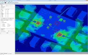 Figure 3. EM visualization
The design workflows for RFICs and mixed-signal ICs are very different from digital IC workflows, as outlined below.
Synthesis
Digital circuits consist of a small number of well-defined logic gates (like NAND). The circuit schematic is converted to a gate-level netlist expressed in a hardware description language like Verilog or very high-speed integrated circuit hardware description language (VHDL). During routing and placement, these gate-level constructs are then converted to on-wafer cells defined by the cell libraries in the selected fab’s process development kit (PDK).
In contrast, RF and mixed-signal ICs are analogue circuits with unique custom designs. The arrangements of resistors, inductors, capacitors, and active components into amplifiers, mixers, or other subsystems are often unique to each IC. They are not readily distillable into standard cells like digital gates are.
Instead, each subsystem is individually converted into on-wafer structures and interconnects. For example, an oscillator may utilise a complex configuration of transistors in feedback loops. The foundry PDKs for RFICs do provide process information, design rules, and models for active and passive components, but they are not as simple or standardised as digital ICs.
Simulation
In digital chip design, the digital nature of signals makes simulations relatively simpler. Digital IC simulations include various digital inputs and timing analyses.
In contrast, RFICs must contend with an infinite set of continuous high-frequency waveforms. Noise, parasitic effects, electromagnetic interference (EMI), and antenna effects emerge from the circuit arrangements as well as the physical on-wafer structures. So, realistic simulations are required at every step throughout the design cycle.
Verification
Design-rule checks (DRC) and implementation using a field-programmable gate array (FPGA) are common in digital IC design.
DRC verification tools are used in RFIC and mixed-signal semiconductor design as well. However, prototyping an RFIC with an FPGA is rare because its RF characteristics will be totally different. FPGAs are still used to verify the digital portions of mixed-signal ICs.
How do you choose the right EDA tool for a wireless electronic design project?
In addition to accurate RF and EM modelling and simulations, an essential feature is the ability to test the designs against wireless standards (like 5G and 802.11ad) right from the start.
This is possible using design tools that include virtual test benches (VTBs) for all the major wireless standards. VTBs ensure that the designs stay within the thresholds that standards place on signal power, noise, interference, and more.
What are the main challenges faced when using EDA tools in complex 3D circuit design?
Some of the main challenges in 3D RF circuit design include:
- modelling electromagnetic behaviours in 3D
- impedance matching
- noise
- linearity
- stability
- power consumption
- electromagnetic interference
- problems caused by increasing densification, like integrating different materials, 3D integration, and advanced packaging
What are the key features to look for in EDA tools for effective RFIC Design?
For effective design of RFICs and mixed-signal ICs, look for these key features:
- Advanced simulation algorithms developed for Keysight RF instrumentation and Keysight RF EDA software ensure equivalent results between virtual simulations and physical measurements.
- Fast-envelope techniques, compact test signals, and distortion EVM make simulation run times practical for RFIC designs in data-intensive, high-bandwidth mmWave or sub-THz applications, including 5G/6G, electric vehicles, and AI-enabled systems.
- Authentic waveforms and VTBs incorporate system context when simulating designs, enabling teams to optimise RFIC designs for their intended system applications sooner and successfully integrate first-pass into physical devices and systems.
Keysight RFIC EDA tools
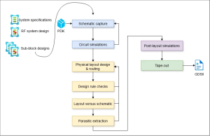 Figure 4. Keysight RFIC EDA tools
Keysight’s ecosystem of EDA tools streamlines RFIC and mixed-signal IC design, simulation, and verification. For large design teams looking for high productivity, the Keysight designcloud enables offloading RF and EM simulations to high-performance cloud platforms for rapid results and quick design cycles. The main design and simulation tools for RFICs and mixed-signal ICs are outlined below.
Keysight Advanced Design System (ADS)
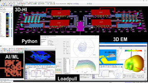 Figure 5. Keysight ADS
The Advanced Design System is tailored for high-frequency RFIC and mixed-signal IC design and simulation. It achieves 3D heterogeneous integration (3DHI) of RFICs, MMICs, packaging, PCBs, and antennas using multi-technology modules. Key features are listed below.
- Multi-technology integration: ADS enables comprehensive 3D integration of chips, packaging, interconnects, and boards, facilitating realistic simulations of assembled products.
- Superior simulation capabilities: The platform’s advanced circuit-level RF simulations and EVM optimisations for mixed-signal ICs produce predictions that are close to real-world measurements.
- Comprehensive component libraries: The platform offers vendor component libraries and PDKs that include symbols and layout footprints, as well as high-accuracy RF and microwave models.
- Standards compliance: ADS enables verification against wireless standards like 5G, automotive radar, and 802.11ad.
- Flexible automation: ADS supports Python scripting for automation and integration with external applications like artificial intelligence (AI) and machine learning (ML) to streamline design and verification workflows.
RFIC Design (RFPro Circuit)
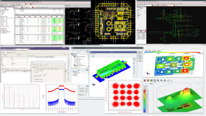 Figure 6. RFPro Circuit
RFPro Circuit is a specialised software for RFIC design. It can:
- model components on silicon chips accurately
- optimise designs with sweeps and load-pull analysis
- simulate RF designs in the Cadence Virtuoso and Synopsys Custom Compiler environments
- increase performance using Monte Carlo and yield analysis
- Assess error vector magnitude (EVM) for the latest communication standards early in the design phase
- Use the latest foundry technology immediately
Keysight RFPro
 Figure 7. RFPro
RFPro enables RFIC and MMIC designers to run interactive electromagnetic-circuit co-simulation for tuning and optimising their circuits. It includes 3D planar and full 3D finite element method EM simulators.
How are AI and ML algorithms integrated into Keysight RFIC EDA tools?
PathWave ADS provides Python application programming interface (API) endpoints for integrating AI frameworks like TensorFlow and PyTorch. This enables the use of advanced artificial neural network models in the design, modelling and simulation workflows.
How is Python integrated with Keysight EDA tools?
Keysight EDA tools provide Python API endpoints that expand custom features and improve usability.
For example, Python scripts can be used to control data analysis, simulators, and processes.
Python scripts enable the training of custom AI-based simulation models that are trained on measured or published data.
The post EDA Tools for Robust RFICs and Mixed-Signal ICs appeared first on ELE Times.
💣 Оголошується конкурс на номінацію «Молодий викладач-дослідник» у 2025 році

Оголошується конкурс на номінацію «Молодий викладач-дослідник» у 2025 році. Заповнені анкети з додатками подаються номінантами до 20 січня 2026 року.
Newbie fixing newbie mistakes.
 | Hey everyone. Just wanted to kinda quickly introduce myself. My dad was always fixing radios, and was a generally great with electronics but he never thought about teaching me (probably because I was always more into art and music idk). Now I'm in my 40's and I decided to get into it, as a kind of connection to my late father, whom I really miss. Last Saturday I fixed my instrument and I bought a DYI tetris handheld and I will teach my son.. or rather we'll learn together. [link] [comments] |
India’s Vision for 6G: Use-Case Driven Innovation and AI-Enabled Networks
Courtesy: Jessy Cavazos, 6G Solutions Expert, Keysight Technology

As the world prepares for the next leap in wireless technology, India is shaping a bold and inclusive vision for 6G, one that goes beyond speed and latency to address real-world challenges. In a recent interview, Mohmedsaeed Mombasawala, Keysight’s General Manager for Industry Solutions in India, and a key contributor to 6G research efforts in India, shared insights into how the country is approaching 6G with a unique blend of pragmatism, innovation, and social impact.
A Use-Case First Philosophy
India’s 6G strategy is fundamentally use-case driven, a departure from traditional infrastructure-first rollouts. Rather than focusing solely on technical specifications or spectrum availability, the country is prioritising solutions that address societal needs, especially in sectors like agriculture, healthcare, and logistics.
This approach is particularly relevant for India’s vast and diverse population, where connectivity gaps persist in rural and remote areas. Mombasawala emphasised that 6G must be more than a technological upgrade: it must be a platform for transformation.
“We’re not just building networks. We’re building solutions for farmers, doctors, and supply chain operators,” he explained.
By anchoring 6G development in real-world applications, India aims to ensure that the technology delivers tangible benefits to communities that have historically been underserved by previous generations of wireless infrastructure.
AI-Native Networks: Intelligence at the Core
One of the most exciting aspects of India’s 6G vision is the emphasis on AI-native radio access networks (RAN). In this model, artificial intelligence isn’t just a tool; it’s a foundational design element. AI will be embedded throughout the network, enabling dynamic spectrum allocation, predictive maintenance, and real-time optimisation of resources.
This shift reflects India’s strength in software and data science, positioning the country to play a key role in intelligent network design. It also aligns with global trends toward more autonomous and adaptive systems, where networks can learn, evolve, and respond to changing conditions without human intervention.
“AI will be central to how we manage, scale, and secure 6G networks,” Mombasawala noted. “It’s not just about efficiency, it’s about enabling new capabilities.”
Spectrum Strategy: Balancing Reach and Performance
While many countries are exploring high-frequency bands for ultra-fast data rates, India is taking a pragmatic approach to spectrum. The focus is on frequency range 3 (FR3) bands, which offer a balance between performance and coverage. These midband frequencies are well-suited for India’s geographic and demographic diversity, allowing for a broader reach without the need for dense infrastructure.
This strategy reflects a deep understanding of India’s connectivity landscape, where rural access remains a critical challenge. By prioritising spectrum that supports ubiquitous coverage, India is ensuring that 6G can serve both urban innovation hubs and remote villages.
Collaborative R&D and Global Engagement
India’s 6G efforts are deeply collaborative, involving academia, startups, industry leaders, and government agencies. Mombasawala highlighted the importance of cross-sector partnerships in driving innovation and ensuring that 6G solutions are both technically robust and socially relevant.
At the same time, India is actively participating in global standardisation efforts, contributing to international dialogues while tailoring its approach to local needs. This dual strategy—global alignment with local customisation—is key to building a 6G ecosystem that is both interoperable and inclusive.
A Blueprint for Inclusive Innovation
India’s vision for 6G offers a compelling blueprint for countries seeking to balance technology innovation with social impact. By focusing on use cases, AI-native design, and inclusive spectrum planning, India is not just preparing for 6G; it’s redefining what 6G can be.
This approach challenges the notion that next-generation technology must be exclusive or elite. Instead, it positions 6G as a tool for empowerment, capable of transforming lives and industries across the socioeconomic spectrum.
“We want 6G to be a catalyst for change,” Mombasawala concluded. “Not just in how we connect, but in how we live, work, and grow.”
The post India’s Vision for 6G: Use-Case Driven Innovation and AI-Enabled Networks appeared first on ELE Times.
Introduction – hardware engineer from China, sharing a custom pulse signal generator
 | Hi everyone, [link] [comments] |
When Silicon Meets the Human Nervous System: A Deep Dive Into Neural Interfaces
Before examining the challenges and opportunities in bioelectronics, it is essential to understand how electronics and the human body converge. The human body—intrinsically organic and biological—can now interact with silicon-based systems through chips, interfaces, and digital extensions that do more than observe; they actively influence physiological function and enable measurable outcomes.
At its core, the human nervous system is among the most sophisticated electrical networks known. Every sensation, movement, and cognitive process originates as an electrical impulse transmitted across billions of neurons. Bioelectronics builds on this foundation by developing electronic systems capable of reading, interpreting, and modulating these neural signals with high precision.
At the centre of this convergence lies neural interface technology—where electronics, materials science, neuroscience, and computation intersect. What began as experimental neural signal recording has evolved into intelligent, closed-loop systems designed to interact with the nervous system in clinically and functionally meaningful ways.
The Nervous System: An Electrical Network
To call the human nervous system an electrical network is to acknowledge the fact that neurons communicate via action potentials—brief voltage changes produced by ionic movement across cell membranes. These electrical impulses propagate along nerve fibres and form the basis of basic human senses, including perception, motion, and cognition.
However, from an engineering standpoint, neural activity resembles a signal source but with certain riders. The biological signals that the neurons communicate through are characterized distinctly from conventional electronic systems in the following ways:
- Extremely low amplitude (microvolt range)
- Highly variable across individuals
- Sensitive to physiological and environmental conditions
- Embedded in a noisy, living medium
These complexities change the entire course of the environment and approach, which is a crucial aspect of the electronics system design, and that’s why bioelectronics is not simply applied electronics—it is fundamentally a new class of system design.
The Neural Interface Challenge
A neural interface is the physical and electrical bridge between living tissue and electronic systems. Basically, it is a technological innovation that enables a direct communication pathway between the brain (nervous system) and an external device, allowing thoughts/neural signals to control machines, and machines to send sensory data back to the brain. Its primary functions are twofold:
- Reading neural signals
- Delivering electrical stimulation
This makes the landscape more challenging, owing to the complex mix of an artificial arrangement to be balanced with a natural or organic system, and making it perform efficiently and adaptively. To this effect, the challenge lies at the interface level itself. Electronics are rigid and static; biological tissue is soft, adaptive, and reactive. Any long-term interface must balance electrical performance with biocompatibility.
Key Challenges in such an arrangement include:
- Mechanical mismatch between electrodes and tissue
- Immune responses that degrade signal quality
- Corrosion in ionic biological environments
- Stability over years, not months
Dr. Ben Rapoport, Co-founder and Chief Science Officer of Precision Neuroscience- the rival of Neuralink, notes that innovation is increasingly focused on minimising invasiveness: “That’s a big misconception, he said. People often incorrectly assume that ‘you need electrodes that penetrate deep inside the brain to get that information out.”
He further adds that Precision lies in developing a thin film that sits on the brain and records the brain activity. This reflects a broader industry trend toward surface-level and flexible neural interfaces rather than deep, rigid implants.
Neural Interfaces Making Gradual Emergence
Industry experts increasingly emphasise that neural interfaces are no longer speculative technologies. Yet these are gradually making space in our lives, making them more common in overall human behavior.
According to Kevin Hughes, Information Scientist of the Chemical Abstracts Service (CAS), which tracks emerging science and engineering domains, “With the recent news that Neuralink is approved to begin human trials, it’s clear that bioelectronics like brain-computer interfaces (BCIs) are moving out of the realm of science fiction and into reality.”
In the very same continuity, he also points out the difference that the industry is witnessing between the number of journals and the number of patents filed in the biotechnology landscape. The following graph shows the starkly lower number of commercial patents, while academic research has outpaced the same in the last 5 years. He writes, “his suggests that large-scale commercialization of these technologies faces fundamental scientific challenges that are being studied at the academic level and may be years away.”
Capturing Neural Signals: An Analog Problem
Neural signal acquisition is fundamentally constrained by analog design challenges. Electrical signals captured at neural electrodes typically exist in the microvolt range, making them highly susceptible to corruption from noise sources such as muscle activity, motion-induced artefacts, electrode impedance variability, and external electromagnetic interference. Unlike many conventional sensing environments, the biological interface itself is dynamic, lossy, and electrically unstable.
To this effect, the front-end electronics gets to play the most decisive role. These must provide:
- Ultra-low-noise amplification
- High input impedance
- Strong common-mode rejection
- Extremely low power operation
Unlike conventional sensors, neural interfaces cannot rely on static calibration. Signal properties drift over time due to biological adaptation and tissue response, demanding adaptive hardware and software co-design. Consequently, effective neural signal acquisition increasingly relies on adaptive architectures, where analog hardware, digital signal processing, and software algorithms are co-designed to track signal drift, compensate for variability, and maintain reliable performance over extended operational lifetimes.
From Signals to Interpretation
Raw neural signals carry no explicit meaning. Interpretation requires computational models capable of identifying patterns associated with intention, perception, or pathology. This has made way for Machine learning, hence making it central to modern bioelectronics. Models must continuously adapt as neural signals evolve, making on-device intelligence essential and timely.
According to BIOS Health, a company focused on AI-driven neural interfaces, this represents a new data modality in medicine:
“At BIOS, we’re developing AI-powered neural interfaces to allow us to read and write neural signals as a new data modality in healthcare… we can decode it, use biomarkers to see how a disease is progressing, and we can change those electrical signals. In doing so, we’ve delivered a therapeutic—we’ve treated a disease.”
This highlights a shift from monitoring systems to active bioelectronic therapies.
Writing to the Nervous System: Electrical Stimulation
Neural interfaces are not limited to passively observing neural activity; they are equally defined by their ability to actively influence the nervous system. This capability is most clearly demonstrated in modern bioelectronic devices that deliver precisely controlled electrical stimulation to targeted neural pathways. By injecting carefully shaped electrical pulses, these systems can alter neural firing patterns in ways that restore, suppress, or modulate biological function.
Electrical stimulation underpins a wide range of therapeutic and functional outcomes, including:
- Restoration of sensory input
- Modulation of dysfunctional neural circuits
- Enablement of motor control
- Suppression of chronic pain signals
From an engineering standpoint, effective neural stimulation demands precise control over parameters such as pulse amplitude, width, frequency, and waveform shape. These parameters must be tailored not only to the targeted neural population but also to long-term safety constraints, including charge balancing and tissue compatibility. Overstimulation risks tissue damage or neural fatigue, making precision and reliability non-negotiable design requirements.
Increasingly, neural stimulation systems are evolving into closed-loop architectures, where real-time sensing, on-device computation, and adaptive stimulation form a continuous feedback cycle. Instead of delivering fixed stimulation patterns, these systems dynamically adjust outputs based on measured neural responses, enabling more personalised, efficient, and clinically effective interventions. This shift from open-loop to closed-loop control represents a critical step toward truly intelligent bioelectronic systems.
Case Study: Cochlear Implants
Cochlear implants remain one of the most successful examples of bioelectronics in practice. Rather than amplifying sound acoustically, cochlear implants convert audio signals into electrical stimulation patterns delivered directly to the auditory nerve. Frequency components are mapped spatially along an electrode array implanted in the cochlea.
Despite delivering a simplified representation of sound, cochlear implants exploit the brain’s neural plasticity. Over time, users learn to interpret these electrical patterns as meaningful auditory experiences. From an engineering perspective, cochlear implants demonstrate:
- Long-term biocompatibility
- Ultra-low-power embedded processing
- Robust signal mapping
- Effective closed-loop adaptation
They validate the principle that bioelectronics succeeds when it works with biology rather than attempting to replicate it perfectly.
Power, Reliability, and Longevity
Implanted bioelectronic systems must operate reliably for years without failure. Power consumption, heat dissipation, and battery safety are critical constraints.
Unlike consumer electronics, failure carries direct clinical risk. As a result, bioelectronic design prioritises stability, redundancy, and conservative validation over rapid iteration.
Conclusion
The future of bioelectronics lies in deeper integration and softer interfaces—flexible electronics, bio-compatible materials, and adaptive systems that learn continuously. As silicon systems become more biologically aware, neural interfaces are evolving from experimental tools into foundational technologies for healthcare and human–machine interaction.
Bioelectronics does not aim to replace the nervous system. It aims to understand it—and, where possible, support it—using electronics designed to operate on biology’s terms.
The post When Silicon Meets the Human Nervous System: A Deep Dive Into Neural Interfaces appeared first on ELE Times.
[OC] CircuiTikZ Visual Editor - Build LaTeX circuits visually in your browser
![[OC] CircuiTikZ Visual Editor - Build LaTeX circuits visually in your browser](https://preview.redd.it/ff4mrezzkdbg1.png?width=640&crop=smart&auto=webp&s=51eca235a4597bcceed580e9f71eb6c86ac3b6a2 "[OC] CircuiTikZ Visual Editor - Build LaTeX circuits visually in your browser") | Hi everyone! I've just uploaded a project I've been working on to GitHub: CircuiTikZ Visual Editor. Link: https://github.com/mangel21/CircuiTikZ-Editor What it doesIt’s a web-based tool designed to make drawing circuits for LaTeX much faster. Instead of typing out coordinates, you can:
Please note that this is a very early version. It's still premature and there are many things to improve (more components, better wire routing, etc.). I am not a developer either, I'm just an electronics engineer who wants to build circuits faster. I would love for you to try it out and see if it helps your workflow. Also, please help improve it. If you are a developer, feel free to contribute or suggest features on GitHub! Let me know what you think! [link] [comments] |
Пам'яті Євгенія Володимировича Кривоногова

26 листопада 2025 року загинув випускник Навчально-наукового машинобудівного інституту 2018 року (кафедра лазерної техніки та фізико-технічних технологій, наразі в складі НН ІМЗ), старший лейтенант Євгеній Володимирович Кривоногов.
LoRaHunt - Monitoring live traps for invasive species
 | Invasive species pose a serious threat to native wildlife and ecosystems. LoRaHunt enables efficient monitoring of live traps, supporting responsible management and relocation efforts. Powered by an ESP32-based Heltec WiFi LoRa 32 (V3), the device primarily operates in deep sleep mode to maximize battery life, achieving up to three months of operation on four 18650 batteries. When a trap is triggered, a reed switch wakes the ESP32 to transmit the event and wait for acknowledgment. Twice-daily heartbeat signals confirm system status, eliminating the need for mandatory manual inspections. [link] [comments] |
Weekly discussion, complaint, and rant thread
Open to anything, including discussions, complaints, and rants.
Sub rules do not apply, so don't bother reporting incivility, off-topic, or spam.
Reddit-wide rules do apply.
To see the newest posts, sort the comments by "new" (instead of "best" or "top").
[link] [comments]
Pages


![[link]](https://i.redd.it/09fgsd68okbg1.jpeg)
![[link]](https://i.redd.it/djpnf0nbahbg1.jpeg)
![[link]](https://i.redd.it/ff4mrezzkdbg1.png)