
Feed aggregator
Space Forge raises £22.6m in Series A funding to accelerate development of ForgeStar-2 and launch of ForgeStar-1
Navitas appoints Cristiano Amoruso to board
Busch integrates centrotherm clean solutions brand into Pfeiffer Vacuum+Fab Solutions
Why the Future of Mobility Depends on Smarter, Smaller Semiconductors
Semiconductors are the crucial parts of electric vehicles (EVs) because they allow for advanced interactive features, efficiency battery management, powertrain enhancements and safety measures. The EV revolution is not only coming; it is currently happening. Semiconductors, a sometimes disregarded yet crucial building element, are the key element of this revolution. These microscopic semiconducting chips are the brain and nervous system of EVs, driving everything from power conversion and battery management to safety systems and intelligent infotainment systems. As EV adoption increases worldwide, demand for high-performance semiconductors is also on the rise making the EV semiconductor market one the most vibrant parts of the tech-led economy.
Market Overview:
Over the last few years, the EV semiconductor industry has seen enormous growth. Based on industry reports, global market size stood at approximately $11.19 billion as of 2023 and is expected to boom to nearly $57.1 billion by 2029 with a CAGR of more than 31%. The boom is being fueled by a combination of factors: tighter environmental controls, government subsidies, growing EV infrastructure and advances in automotive electronics technology.
EVs need significantly more semiconductor devices compared to conventional internal combustion engine (ICE) cars. From motor control units and battery management units (BMUs) to infotainment systems and advanced driver-assistance systems (ADAS), semiconductors make these features functional.
Key Technologies Driving Growth
Among the most prominent trends driving the market is the trend towards wide-bandgap semiconductors, specifically Silicon Carbide (SiC) and Gallium Nitride (GaN) materials. These materials are superior to conventional silicon for high-temperature and high-voltage applications and hence, they are suited for EV powertrains as well as rapid-charging infrastructure.
SiC chips, for instance, have the potential to make inverters more efficient, thus extending driving ranges and cutting energy loss. Players such as STMicroelectronics, Infineon, Wolfspeed and ON Semiconductor are investing heavily in SiC lines to address this increasing demand.
Since they allow producers to integrate several functions into a single chip and reduce the size and weight of their parts, system on chip (SoC) solutions are gaining popularity as well. This enhances overall car performance and design versatility.
Uses:
- In EVs, semiconductors are crucial to the vehicle’s battery management system (BMS). They assist in keeping an eye on the battery pack’s temperature, health and charge level. Onboarding charging systems also use semiconductors to help convert and control voltage, which improves charging speed and efficiency.
- Advanced driver assistance systems (ADAS) based primarily on semiconductor processors are adaptive cruise control, lane-keeping assist, and collision avoidance systems. These circuits make decisions in real time using data from multiple sensors, cameras, and radar.
- Infotainment systems are driven by semiconductor chips, incorporating features such as touchscreen display, GPS navigation, car audio, and connectivity features of the smartphone.
- As the largest, with more than half of the market, is the powertrain segment. Power semiconductors control battery power so that the electric motor can operate efficiently.
Regional Perspectives: Asia-Pacific Leads
Geographically, South Korea, Japan and China dominate the Asia-Pacific EV semiconductor market.
With schemes such as “Make in India” and the FAME II scheme (Faster Adoption and Manufacturing of Hybrid and Electric Vehicles) encouraging domestic EV and semiconductor manufacturing, India is also becoming a key player.
In addition to that, Europe is also deeply investing in environmental-friendly transport as well as in semiconductor technology. With the CHIPS and Science Act, America is also strengthening its domestic production of semiconductors to try to meet its demand less on foreign chipmakers and foster a stronger EV ecosystem.
Challenges and Supply Chain Constraints
Though there is a strong growth prognosis, the market does not lack its challenges. The most critical of these is the semiconductor supply chain crisis that commenced with the onset of the COVID-19 pandemic and has since impacted industries across the globe. The highly concentrated nature of chip production—dominated by just a handful of foundries such as TSMC (Taiwan) and Samsung (South Korea)—creates vulnerabilities.
Furthermore, geopolitical tensions, most notably between the U.S. and China, are recasting global trade patterns. China’s dominance of the supply chain of rare earth minerals like gallium and germanium, critical to semiconductor manufacturing, constitutes a strategic risk for the West and has fueled demands for diversification of sources.
Market volatility is also a problem. For example, firms such as Mersen and STMicroelectronics have recently pushed back their semiconductor revenue targets owing to volatile EV demand and postponed ramp-up of new plants. Analysts now estimate that key financial milestones will be achieved by 2029–2030, rather than previous estimates of 2026–2027.
Conclusion:
The EV Semiconductor industry sits at the confluence of mobility digitalization and transport electrification, with the demand growing at an unprecedented level. Recent data indicates that the sales of EVs worldwide will surpass 20 million units by 2025, representing one in four automobiles sold globally. The growth is fueled by heightened affordability, decreased operating expenses and government support.
Further, the market for compound semiconductor materials, comprising Silicon carbide (SiC) and Gallium Nitride (GaN) is estimated to increase from $29.97 billion in 2025 to $91.03 billion in 2025, driven by the growth of 5G and EV adoption. The overall semiconductor market is estimated to be $ 697 billion in 2025, representing an 11% year-over year growth rate.
Despite supply chain risks and market instability, improvements in production, materials and system integration will continue to advance the field. Technology specialists, investors, and manufacturers view this industry as having a high rate of return and playing a key role in shaping the direction of mobility in the future.
The post Why the Future of Mobility Depends on Smarter, Smaller Semiconductors appeared first on ELE Times.
Офіційне повідомлення

Наразі у деяких спільнотах у соціальних мережах поширюється фейкова інформація, що у КПІ ім. Ігоря Сікорського до складу екзаменаційних комісій нібито почали включати представників Територіальних центрів комплектування та соціальної підтримки (ТЦК СП).
Transforming Chip Design with Agentic AI: Introducing Cadence Cerebrus AI Studio
The industry’s first agentic AI, multi-block, multi-user SoC design platform.
Cadence has launched Cadence Cerebrus AI Studio. It is the industry’s first agentic AI multi-block multi-user design platform, significantly accelerating an entire system-on-chip’s (SoC) time to market by 5X.
Recent technological advancements have led to semiconductor chips with intricate functionalities requiring trillions of transistors. These chips must support high-performance computing and be designed using advanced process nodes. Cadence Cerebrus AI Studio is a state-of-the-art SoC agentic AI design implementation tool that can help achieve ambitious power, performance, and area (PPA) goals and reduce turnaround time for highly sophisticated chips.
Cadence Cerebrus AI Studio is aligned with Cadence’s Intelligent System Design strategy. For block-level AI-driven optimization, Cadence Cerebrus Intelligent Chip Explorer was released in 2021 and has successfully been used in hundreds of production designs. Cadence Cerebrus AI Studio is the next generation of AI-driven digital implementation products using the most advanced agentic AI technology for implementing an entire SoC or subsystem, enabling a generational shift from multiple designers optimizing a single block to multiple blocks being designed by a single engineer.
Utilizing the latest agentic AI system that features autonomous AI agents capable of making decisions and taking multi-step actions based on high-level objectives, Cadence Cerebrus AI Studio can orchestrate the complete chip implementation flow delivering engineering productivity benefits. The Innovus integrated RTL synthesis and implementation platform, including Python scripting and a large language model (LLM) AI assistant, provides completely automated design realization.
Key features of Cadence Cerebrus AI Studio include:
- Intelligent Agentic AI Workflows: Employs AI agents that manage design optimization methodologies, resulting in unparalleled PPA and accelerated design closure.
- Multi-Block, Multi-User Design Infrastructure: A central design platform empowers a single engineer to design multiple blocks, allowing for more µm2 of SoC implementation per engineer.
- Hierarchical Design Optimization: Top-block co-optimization using AI greatly reduces manual work and enables faster design closure.
- Advanced Data Analytics: AI-driven data platform facilitates smarter and faster design debug by quickly identifying bottlenecks and critical paths.
- Customizable Live Dashboard: Facilitates collaboration and knowledge sharing across designs and projects, resulting in exponential productivity benefits.
“We are thrilled to launch Cadence Cerebrus AI Studio, the industry’s first agentic AI SoC design platform, built on the solid foundation of established Cadence digital implementation tools. This tool extends the AI technology to hierarchical SoC design implementation, exponentially multiplying the PPA and productivity gains while addressing the engineering workforce shortage,” says Chin-Chi Teng, senior vice president and general manager, Digital & Signoff Group at Cadence. “Cadence Cerebrus AI studio, which leverages the latest agentic AI technology, is very well equipped to achieve unparalleled PPA, fastest time to design targets, and game-changing engineering efficiency.”
The post Transforming Chip Design with Agentic AI: Introducing Cadence Cerebrus AI Studio appeared first on ELE Times.
Keysight and SPHEREA Join Forces to Strengthen European Aerospace and Defense Testing Capabilities
- Provides access to strategic sovereign European programs with EU-designed, EU-built systems
- Enables locally developed solutions that are trusted, modular, and interoperable
- Integrates critical modular technology that enables next-generation measurement capabilities
Keysight Technologies, Inc. has collaborated with SPHEREA to offer customers improved testing capabilities in the aerospace and defense (A&D) sector. By joining forces, Keysight will combine its expertise in high-performance electronics tests and measuring systems with SPHEREA’s design and integration capabilities, to support the shifting requirements in the A&D space.
As European nations increasingly prioritize defense independence and aim to remain compliant with stringent export control regulations, this collaboration offers a timely and strategic response to these needs. The deployment of next-generation measurement technologies is critical to national security, but it is also essential to align with the need for EU-designed solutions to support self-sufficient and strategic autonomy.
Keysight and SPHEREA are working together to address this challenge, providing customers with local solutions that are built on trusted technology. As part of the agreement, the deployment includes the delivery of Keysight’s Radar Target Generator and Electronic Warfare testing solutions, featuring frequency expansion from 18 GHz to 40 GHz, which led to a successful tender for a leading military alliance. The solution consists of Keysight’s AXIe-based high-performance embedded controller with low latency and signal processing, arbitrary waveform generation, and its latest low phase-noise synthesizers.
“Our partnership with SPHEREA enables us to deliver an innovative, scalable solution. The accurate radar test solution is designed with our European R&D expertise, and delivery capabilities to provide future-ready tests that meet the evolving needs of our defense customers,” said Thierry Locquette, EMEA VP and GM at Keysight.
“We are proud to cooperate with Keysight using our deep RF expertise to develop the commercial off the shelf (COTS) Up and Down Converter with 1 GHz bandwidth in a short time frame. Together, we fulfilled the customer’s needs for advanced capability within a condensed timeline,” said Julien Pulice, Group CTO Deputy at SPHEREA.
The post Keysight and SPHEREA Join Forces to Strengthen European Aerospace and Defense Testing Capabilities appeared first on ELE Times.
MRAM and ReRAM: The quest for automotive, aerospace niches

Where do MRAM and ReRAM technologies stand after years of promise to replace incumbent memories? Gary Hilson speaks to MRAM and ReRAM makers as well as an industry analyst to find the truth about their market standing. While these memory technologies offer endurance, they don’t seem to compete on price. As a result, they are eying specialized markets like automotive and aerospace to remain relevant.
Read the full story at EDN’s sister publication, EE Times.
Related Content
- ReRAM enhances edge AI
- ReRAM Machine Learning Embraces Variability
- An MCU test chip embeds 10.8 Mbit STT-MRAM memory
- Memory lane: Where SOT-MRAM technology stands in 2024
- Emerging Memories May Never Go Beyond Niche Applications
The post MRAM and ReRAM: The quest for automotive, aerospace niches appeared first on EDN.
Практикум-тренінг для викладачів закладів професійної освіти

У нашому університеті відбувся навчальний практикум-тренінг для викладачів закладів професійної (професійно-технічної) освіти щодо впровадження курсу «Встановлення сонячних фотоелектричних систем».
На війні загинув випускник нашого університету Олег Аксьоненко

На війні загинув випускник нашого університету Олег Аксьоненко (30.08.1993 – 04.01.2025). У 2010 році Олег вступив на факультет електроніки (кафедра акустики), у 2014 році отримав диплом бакалавра і у 2016 році диплом спеціаліста.
Finwave raises $8.2m in bridge investment to fuel market push
FM Radio receiver
 | I have made a schematic of analog FM receiver!! [link] [comments] |
Asynchronous BCD Counter
 | submitted by /u/Kotsaros [link] [comments] |
Seven-octave linear-in-pitch VCO

Frequent contributor Nick Cornford recently shared design ideas incorporating cool circuits for linear-in-pitch voltage-controlled oscillators (LPVCOs):
- Revealing the infrasonic underworld cheaply: Part 1 and Part 2
- A pitch-linear VCO: Part 1 and Part 2
Wow the engineering world with your unique design: Design Ideas Submission Guide
The linear in pitch function, which makes output frequency proportional to the antilog of voltage, is interesting because it provides a better perceptual interface to the inherently logarithmic human ear than a linear frequency.
One measure of the performance of an LPVCO is its octave range. That’s the ratio of highest to lowest frequency that its output spans, expressed as the binary (base 2) logarithm of the ratio. Two octaves (22 = 4:1) is good. Three octaves (23 = 8:1) is better. The LPVCO in Figure 1 does seven (27 = 128:1).

Figure 1 A seven-octave LPVCO comprises Q1 Q2 antilog pair that converts the 0 V to 5 V Vin, to a 1 µA to 128 µA Ic2, for a proportional 27 = 128:1 change in C1 ramp rate and U1 oscillation frequency. Counter U2 then scales the U1 oscillation frequency by 4 and converts to a three-level, very vaguely “sine-ish,” output waveform.
Here’s how it works.
Control voltage Vin is scaled by a voltage divider (R1/R2 + 1) = 34:1 and applied to the Q1 Q2 exponential-gain current mirror. There, it is level-shifted and temperature-compensated by Q1, then anti-logged by Q2 to produce
Ic2 = 2(1.4Vin) µA. The resulting C1 timing ramp spans from 5 ms (for Vin = 0) to 40 µs (for Vin = 5 V). The ramp ends when it crosses analog timer U1’s 1.67-V trigger level and is reset via R5 and D1 to U1’s threshold level of 3.33 V, starting another oscillation cycle. The resulting sawtooth will therefore repeat at F = Ic2/(1.67C2) = 2(1.4Vin) µA / 5nCb = 200 (2(1.4Vin) ) Hz.
Nick’s lovely designs show that short pulses such as U1’s output spikes require conversion to a waveshape with a less intense harmonic content if we want to hear a listenable audio output. Therefore, U2’s switch-tail counter divides U1’s oscillation frequency by 4. This produces a hardly sinusoidal, but at least somewhat less annoying, tri-level 50 Hz to 6400 Hz final output.
Thanks go to Nick for a fun and well-conceived design topic, and of course to editor Aalyia for her friendly Design Idea department format that makes such enjoyable collaboration possible!
Stephen Woodward’s relationship with EDN’s DI column goes back quite a long way. Over 100 submissions have been accepted since his first contribution back in 1974.
Related Content
- Revealing the infrasonic underworld cheaply, Part 1
- Revealing the infrasonic underworld cheaply, Part 2
- A pitch-linear VCO, part 1: Getting it going
- A pitch-linear VCO, part 2: taking it further
- Can a free running LMC555 VCO discharge its timing cap to zero?
The post Seven-octave linear-in-pitch VCO appeared first on EDN.
Казковий і предметний світи Като Лукач

В університетському Державному політехнічному музеї ім. Бориса Патона 24 квітня відкрито виставку "Казковий світ ілюстраторки і графіка Като К.Лукач". На ній представлено твори відомої художниці-графіка, дизайнерки та рекламістки ХХ століття, і сьогодні дуже популярної в Угорщині. Виставку приурочено до 125-ліття від дня її народження.
Porotech leading ‘One-Stop AR Solution Alliance’ to accelerate AR commercialization
III-V Epi celebrates fifth anniversary
TOP 10 Mouse brands in India
Introduction
The computer mouse is a crucial tool for both work and playing games. Many brands are creating special designs to make using them better. In India, there is a wide variety of mice that suit different needs, such as professional tasks, simple internet browsing, or playing games competitively. This article will look at top 10 mouse brands available today. It will discuss where each brand began, highlight their main features, and also mention some of their popular model.
- Logitech
Logitech, a swiss-based company, is known for its excellent computer peripherals, with top-selling mouse models like Logitech B170, M186, and G502(Gaming). Famous for its excellent computer peripherals, Logitech mice offer ergonomic shapes, precise tracking, and long battery life. Top-selling models are Logitech B170, M186, and G502(Gaming).
- HP
HP, which has its base in the United States, offers reliable office and gaming mice like the HPX200 Wireless Mouse and OMEN Vector (Gaming). Offers reliable office and gaming mice with smooth silky performance, adjustable DPI adjustment, and wireless-connectivity. Best models include HPX200 Wireless Mouse and OMEN Vector (Gaming).
- Dell
Dell, a US company, provides affordable and efficient mice like Dell MS 116 (Wired) and Alienware AW610M (Gaming). Provides affordable mice with plug-and play ease, LED tracking, and tough build. Top models are Dell MS116 (Wired) and Alienware AW610M(Gaming).
- Lenovo
Lenovo is a Chinese organization which produces stylish and ergonomic mice like Lenovo Legion M200 (Gaming) and Yoga Mouse. Designs stylish and ergonomic mice with DPI sensor, ambidextrous design, and wireless Bluetooth connectivity. Both models are Lenovo Legion M200(Gaming) and Yoga Mouse.
- Zebronics
Zebronics, which is an Indian brand, offers budget- priced mice such as Zebronics Zeb-Jaguar and Blanc Slim. Indian brand known for budget-priced silent click, DPI- adjustable mice with elegant looks. Its top models include Zebronics Zeb-Jaguar and Blanc Slim.
- Redragon
Redragon, a Chinese company, specializes in gaming peripherals, with products such as the Redragon M808 Storm and Cobra M711. Specializes in gaming peripherals with customizable buttons, RGB lights, ultra-fast sensors, and high DPI. Best-selling products include Redgraon M808 Storm and Cobra M711.
- Razer
Razer Inc. is a global technology firm that deals in gaming hardware, consumer electronics. It is dual headquartered in Singapore and Irvine, California, USA. Razer is renowned for its high-performance gaming peripherals, such as mice, keyboards, headsets, and laptops. A high-end gaming brand, providing high-performance mice with ultra-high- performance mice with ultra-sensitive sensors, programmable RGB lighting, and programmable buttons. Famous models are Razer DeathAdder V2 and Basilisk X Hyperspeed.
- Apple
Apple’s mouse line comes from the United States, originally founded in 1976. Apple mice have come a long way, from the one-button Lisa Mouse in 1983 to the Magic Mouse 2, which brought laser tracking and multi-touch gestures. The newest iteration, the Magic Mouse, is a wireless, rechargeable mouse that features a multi-touch surface through which the user can swipe back and forth between web pages. Apple revised the Magic Mouse in 2024 with a USB-C port, replacing the earlier Lightning connector.
- Microsoft
Microsoft’s mouse logo has its origins in the United States, as Microsoft was founded in 1975. Microsoft first launched a mouse in 1983, which had a steel ball for tracking. The newest models are the Surface Arc Mouse, an ultra-slim, lightweight mouse, it is connected via Bluetooth and includes a touch surface that allows users to scroll vertically or horizontally. Microsoft Pro IntelliMouse, which is right-handed, includes a 16000 DPI resolution, and includes high-speed tracking.
10. Corsair
Corsair is an American corporation based in Milpitas, California, USA. The organization majors in gaming hardware, peripherals with high performance, computer parts, and accessories like keyboards, mice, power supply units, coolers and streaming devices. Deals in gaming peripherals, with mice having high DPI optical sensors, programmable macros, and ergonomic grips. Famous models are Corsair Harpoon RGB and Dark Core Pro.
The market share distribution of mouse brands In India is as follows:
|
Brands |
Market Share % |
|
Logitech |
25% |
| HP | 18% |
| Dell | 15% |
| Razer | 10% |
|
Zebronics |
8% |
| Lenovo | 7% |
| Corsair | 5% |
|
Redragon |
4% |
|
Microsoft |
5% |
| Apple | 3% |
|
|
Conclusion
India’s market for computer mouse is growing at a steady pace, fuelled by rising demand for wireless and ergonomically-designed mice. The market for computing mouse is expected to expand by USD 3.43 billion from 2024 to 2029, at a Compound Annual Growth Rate (CAGR) of 14.1%. Top brands like Logitech, HP, and Dell continue to dominate the professional and high-end segments, while local brand like Zebronics cater to cost conscious customers with value-added offerings.
The post TOP 10 Mouse brands in India appeared first on ELE Times.
Add-on features in electronic products: The good part

Add-on features are all the rage in electronic products. But are they actually handy or just embody bells and whistles? What’s their hardware and software cost? And more importantly, do they serve an actual value or merely add to the user-experience clutter? Bill Schweber looks at this user interface mystery and finds some answers.
Read the full story at EDN’s sister publication, Planet Analog.
Related content
- Coffee Teardown: Simple, Effective Design
- What’s the Impact of Medical-Design Mandates?
- Soft on/off is designer’s dilemma, user’s headache
- Extreme Analog Design: Don’t Forget Those Passives
- AVAS and the dilemma of ‘too good to be true’ designs
- Instrumented Hockey Puck is an Extreme Analog Design
- With so many mandates, can we still deliver a product design?
The post Add-on features in electronic products: The good part appeared first on EDN.
TeseoVI: ST’s 1st single-die quad-band GNSS receiver makes autonomous driving mainstream
ST is launching the TeseoVI, our first single-die quad-band GNSS receiver, which also features anti-jamming and anti-spoofing technologies. As car makers demand more precision and reliability for applications like level 2 and level 3 autonomous driving, we also wanted to lower costs to make those technologies even more accessible to mainstream vehicles. Indeed, by offering a single-die system, we can significantly lower the bill of materials without compromising the smarter capabilities car makers bring to their drivers. The TeseoVI also features a pin-to-pin compatibility between its safety-capable (ASIL-B) and non-safety versions for greater design flexibility.
TeseoVI: Moving to a single die Why is a single die a challenge?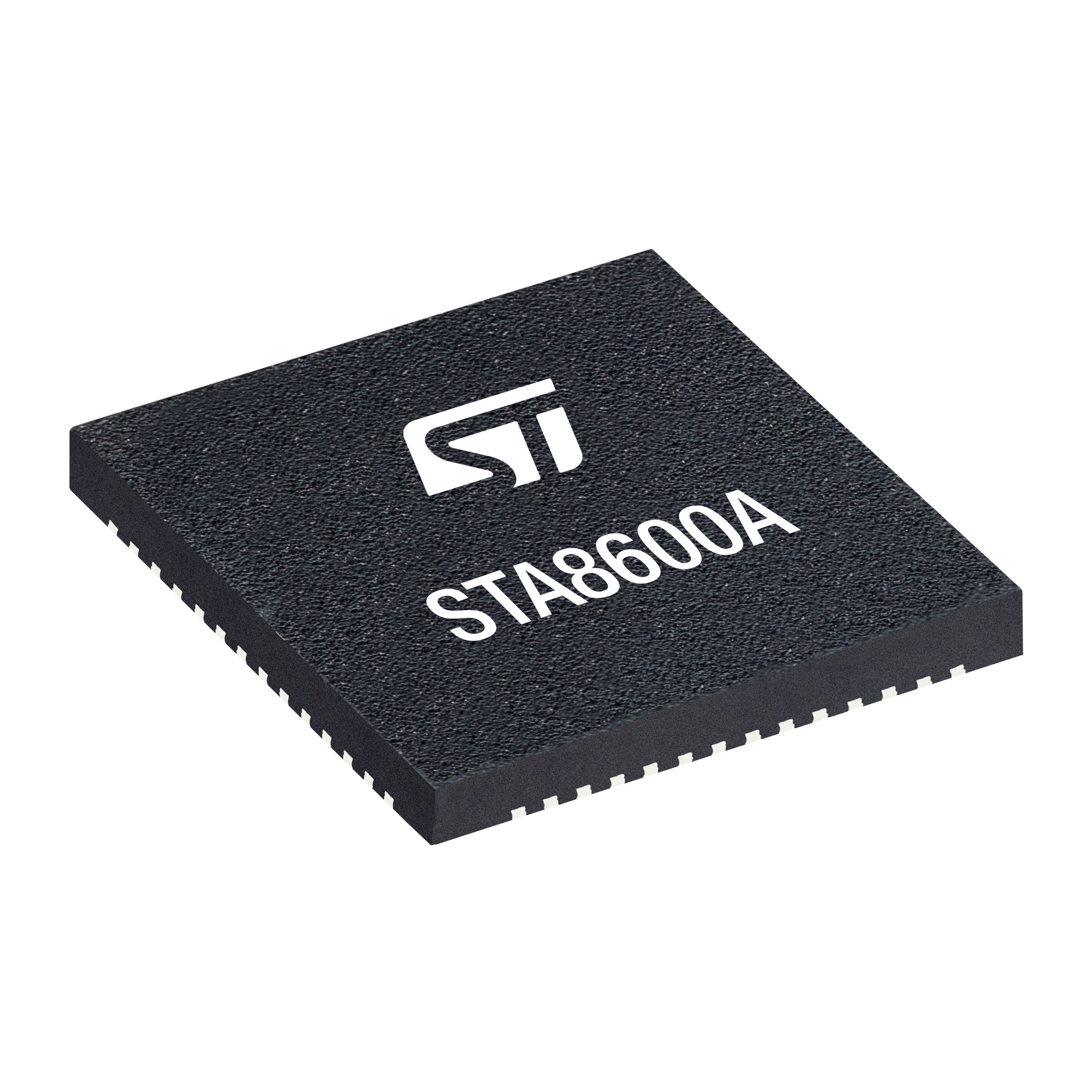 TeseoVI (STA8600A) in a VFQFPN package
Most GNSS receivers for automotive feature multiple dies in one package. There’s the digital microcontroller, a baseband radio, and sometimes a third die for memory. The industry adopted this approach because it bypassed significant manufacturing challenges that come from putting everything on the same die. Moreover, adding enough memory can also lead to a big die size, lowering yields and making devices more expensive. Using multiple dies also makes optimizing the RF easier, which leads to greater precision. Single-die GNSS receivers are typical in smartphones and much smaller systems that don’t require as much accuracy but have remained a problem for cars.
How did TeseoVI overcome this challenge?That’s why the TeseoVI is special. It brings the convenience and cost-effectiveness of the single-die approach that’s so popular on smartphones while overcoming the precision and reliability challenges that prevented such an approach from serving cars. To make this possible, ST optimized the RF and the phase-change memory (PCM), among other things. For the former, we employed a new generation of baseband processing, opening the door to new features (more on that later).
TeseoVI: Jamming protection What are the L1 and L5 signal bands?One of the features brought on by the new baseband processor is the ability to track L1 and L5 signals independently. L1 is the oldest GNSS signal, using a frequency of 1575.2 MHz. It’s the slowest and doesn’t travel well through obstacles, but its maturity means it is a preferred signal for most satellite positioning applications. L5 uses the 1176 MHz frequency and is the most advanced GNSS signal. Launched in 2021, it targets critical applications, like aviation, but is also available for consumer systems. It offers greater bandwidth thanks to higher power levels, improved accuracy thanks to interference rejection, and better robustness. Indeed, thanks to its lower frequency, it features a longer wavelength that deals better with obstacles.
How to jam the L1 signal?Another reason supporting L1 and L5 signals independently is essential is because it provides anti-jamming protection. Jamming happens when a signal overwhelms the receiver. It can result from unintentional electromagnetic interference from antennas or large infrastructure emitting intense radiation. There are also dedicated jammers to bypass fleet monitoring, insurance trackers, and more. The L1 frequency is very easy to jam. It doesn’t have redundancy features, and its low signal strength is easy to overwhelm, which causes the GNSS receiver to lose its lock on the signal, thus failing to acquire navigation data. It’s so easy that L1 jammers, although illegal in most countries, may cost less than US$20, according to The Resilient Navigation and Timing Foundation.
TeseoVI and anti-jammingInterestingly, even GNSS receivers that track L5 signals may require the L1 signal. Indeed, many devices acquire timing data from the L1 signal during their boot sequence and then use it to lock onto the L5 signal. The problem is that even a low-cost jammer could prevent a device from acquiring data from the L1 signal, meaning the receiver can’t use the L5 band. The new baseband processing in the TeseoVI introduced an L5-only mode, meaning it doesn’t need L1 to acquire data on L5. Consequently, it can bypass jammers. Additionally, L5 is so robust some estimate it to be 30 times harder to jam than L1.
TeseoVI: Spoofing protection How to spoof a GNSS signal?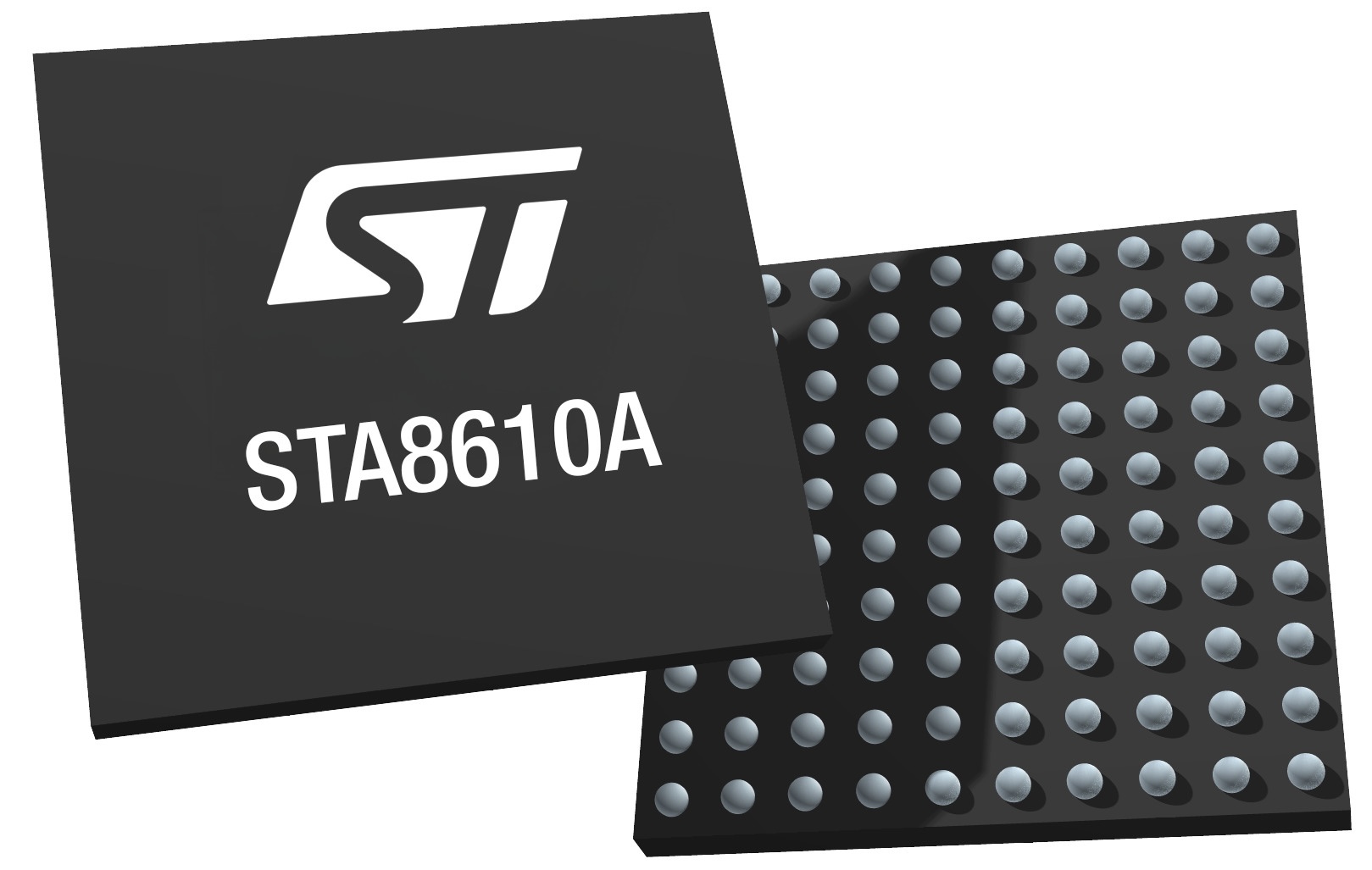 TeseoVI+ (STA8610A)
The new TeseoVI also supports the open service navigation message authentication (OSNMA) from the Galileo constellation. In a nutshell, the feature prevents spoofing attacks by cryptographically authenticating the source of a message. Very simply, the technology uses a message authentication code (MAC) to guarantee the authenticity of a signal’s provenance. It doesn’t encrypt the whole message but sends a series of codes, which is a far more efficient use of the bandwidth. Consequently, since Galileo generates the code, hackers can’t fake it. Additionally, since the standard sends multiple codes over time, hackers can’t just grab one key and reuse it in a replay attack. By the time they do so, the key has expired.
How to support OSNMA?To support OSNMA, hardware manufacturers must update their firmware and their software stack and offer enough processing power to handle the extra computations. This is why ST also provides extensive software implementations with its GNSS receivers. We know that taking advantage of new features can be complex. In this instance, decoding the OSNMA fields and managing the keys requires complex libraries that must pass audits and receive regular updates. Hence, the TeseoVI not only supports this anti-spoofing technology but enables developers to take advantage of it in their applications rapidly.
Making multiband more accessible More advanced features to mainstream cars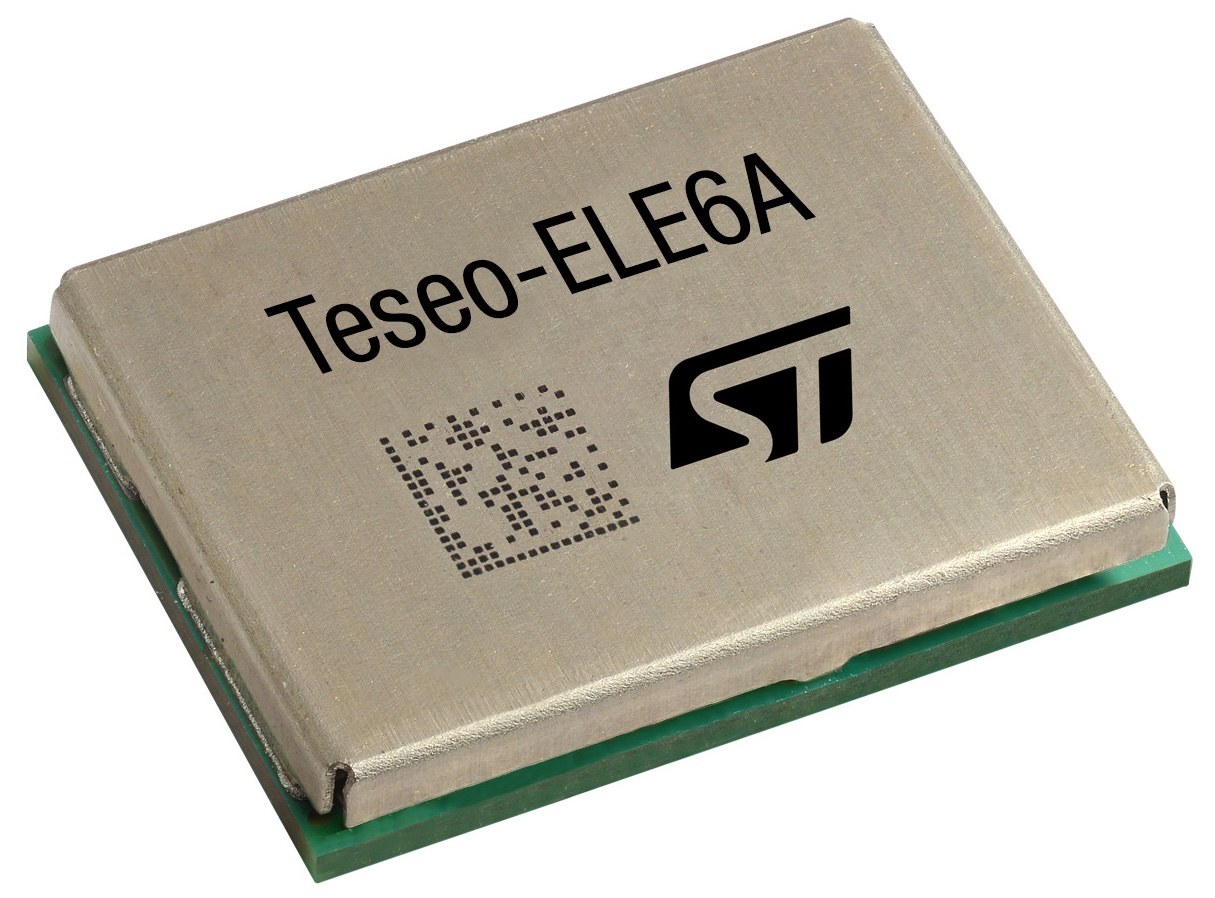 Teseo-ELE6A
One of the greatest benefits of a single-die design is the ability to lower the cost of materials. In fact, since there’s no need for external RF and external memory, engineers may target a BOM cost of about a dollar. Obviously, this is only a general reference point. In practice, the price will vary based on the complexity of the design and volumes. However, in all cases, it means that previous customers who used to avoid multiband solutions because they were too expensive will now be able to jump on the bandwagon. For instance, we can expect level 2 and 3 autonomous driving features to reach more mainstream vehicles.
More flexibility to integrators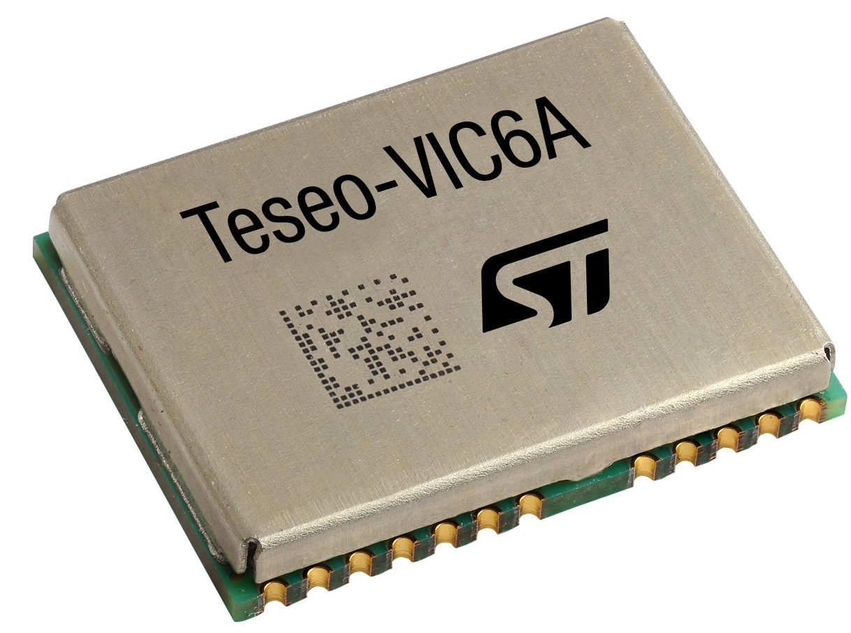 Teseo-VIC6A
The TeseoVI is also the first GNSS receiver for automotives to have a pin-to-pin compatible version for safety applications, the TeseoAPP2 (STA9200MA), which features the same QFN56 package as the TeseoVI (STA8600A). As a result, developers can simply create one reference design and switch between the ASIL-certified and the non-certified part number, depending on their needs.
ST will also be offering the TeseoVI+ (STA8610A). It’s the same device as the TeseoVI, but the TeseoVI+ can welcome custom algorithms thanks to dual M7 Core Processing and External Memory Interface (Flash/RAM). Hence, teams wanting to use their application can do away with our positioning and measurement software. Finally, we also offer a module with a 6-axis inertial sensor, the Teseo-VIC6A, and its safety alter ego, the Teseo-ELE6A.
The post TeseoVI: ST’s 1st single-die quad-band GNSS receiver makes autonomous driving mainstream appeared first on ELE Times.
Pages


![[link]](https://i.redd.it/yowh03wh4s0f1.png)
![[link]](https://i.redd.it/7dgg17s1wr0f1.png)