
Feed aggregator
Add-on features in electronic products: The good part

Add-on features are all the rage in electronic products. But are they actually handy or just embody bells and whistles? What’s their hardware and software cost? And more importantly, do they serve an actual value or merely add to the user-experience clutter? Bill Schweber looks at this user interface mystery and finds some answers.
Read the full story at EDN’s sister publication, Planet Analog.
Related content
- Coffee Teardown: Simple, Effective Design
- What’s the Impact of Medical-Design Mandates?
- Soft on/off is designer’s dilemma, user’s headache
- Extreme Analog Design: Don’t Forget Those Passives
- AVAS and the dilemma of ‘too good to be true’ designs
- Instrumented Hockey Puck is an Extreme Analog Design
- With so many mandates, can we still deliver a product design?
The post Add-on features in electronic products: The good part appeared first on EDN.
TeseoVI: ST’s 1st single-die quad-band GNSS receiver makes autonomous driving mainstream
ST is launching the TeseoVI, our first single-die quad-band GNSS receiver, which also features anti-jamming and anti-spoofing technologies. As car makers demand more precision and reliability for applications like level 2 and level 3 autonomous driving, we also wanted to lower costs to make those technologies even more accessible to mainstream vehicles. Indeed, by offering a single-die system, we can significantly lower the bill of materials without compromising the smarter capabilities car makers bring to their drivers. The TeseoVI also features a pin-to-pin compatibility between its safety-capable (ASIL-B) and non-safety versions for greater design flexibility.
TeseoVI: Moving to a single die Why is a single die a challenge?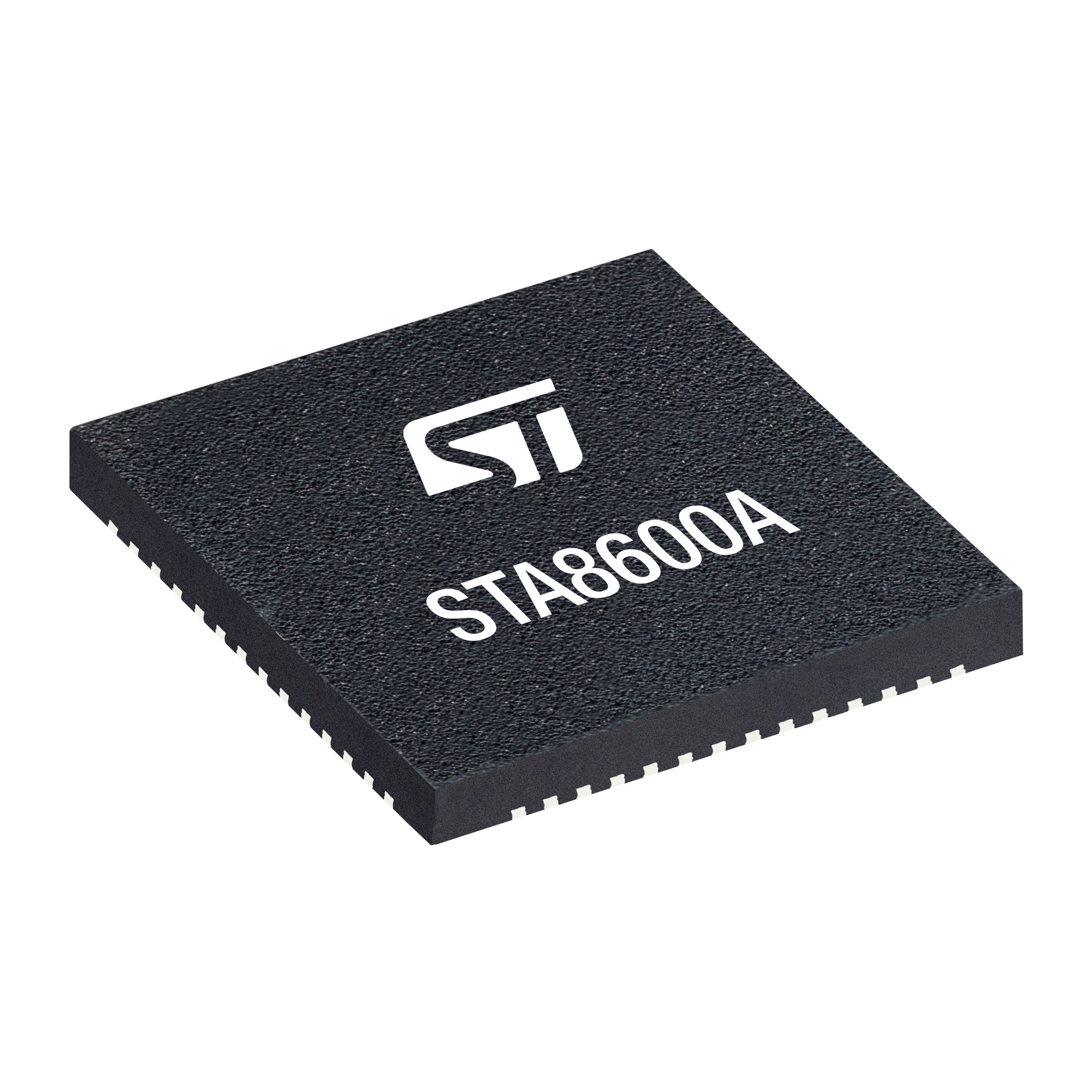 TeseoVI (STA8600A) in a VFQFPN package
Most GNSS receivers for automotive feature multiple dies in one package. There’s the digital microcontroller, a baseband radio, and sometimes a third die for memory. The industry adopted this approach because it bypassed significant manufacturing challenges that come from putting everything on the same die. Moreover, adding enough memory can also lead to a big die size, lowering yields and making devices more expensive. Using multiple dies also makes optimizing the RF easier, which leads to greater precision. Single-die GNSS receivers are typical in smartphones and much smaller systems that don’t require as much accuracy but have remained a problem for cars.
How did TeseoVI overcome this challenge?That’s why the TeseoVI is special. It brings the convenience and cost-effectiveness of the single-die approach that’s so popular on smartphones while overcoming the precision and reliability challenges that prevented such an approach from serving cars. To make this possible, ST optimized the RF and the phase-change memory (PCM), among other things. For the former, we employed a new generation of baseband processing, opening the door to new features (more on that later).
TeseoVI: Jamming protection What are the L1 and L5 signal bands?One of the features brought on by the new baseband processor is the ability to track L1 and L5 signals independently. L1 is the oldest GNSS signal, using a frequency of 1575.2 MHz. It’s the slowest and doesn’t travel well through obstacles, but its maturity means it is a preferred signal for most satellite positioning applications. L5 uses the 1176 MHz frequency and is the most advanced GNSS signal. Launched in 2021, it targets critical applications, like aviation, but is also available for consumer systems. It offers greater bandwidth thanks to higher power levels, improved accuracy thanks to interference rejection, and better robustness. Indeed, thanks to its lower frequency, it features a longer wavelength that deals better with obstacles.
How to jam the L1 signal?Another reason supporting L1 and L5 signals independently is essential is because it provides anti-jamming protection. Jamming happens when a signal overwhelms the receiver. It can result from unintentional electromagnetic interference from antennas or large infrastructure emitting intense radiation. There are also dedicated jammers to bypass fleet monitoring, insurance trackers, and more. The L1 frequency is very easy to jam. It doesn’t have redundancy features, and its low signal strength is easy to overwhelm, which causes the GNSS receiver to lose its lock on the signal, thus failing to acquire navigation data. It’s so easy that L1 jammers, although illegal in most countries, may cost less than US$20, according to The Resilient Navigation and Timing Foundation.
TeseoVI and anti-jammingInterestingly, even GNSS receivers that track L5 signals may require the L1 signal. Indeed, many devices acquire timing data from the L1 signal during their boot sequence and then use it to lock onto the L5 signal. The problem is that even a low-cost jammer could prevent a device from acquiring data from the L1 signal, meaning the receiver can’t use the L5 band. The new baseband processing in the TeseoVI introduced an L5-only mode, meaning it doesn’t need L1 to acquire data on L5. Consequently, it can bypass jammers. Additionally, L5 is so robust some estimate it to be 30 times harder to jam than L1.
TeseoVI: Spoofing protection How to spoof a GNSS signal?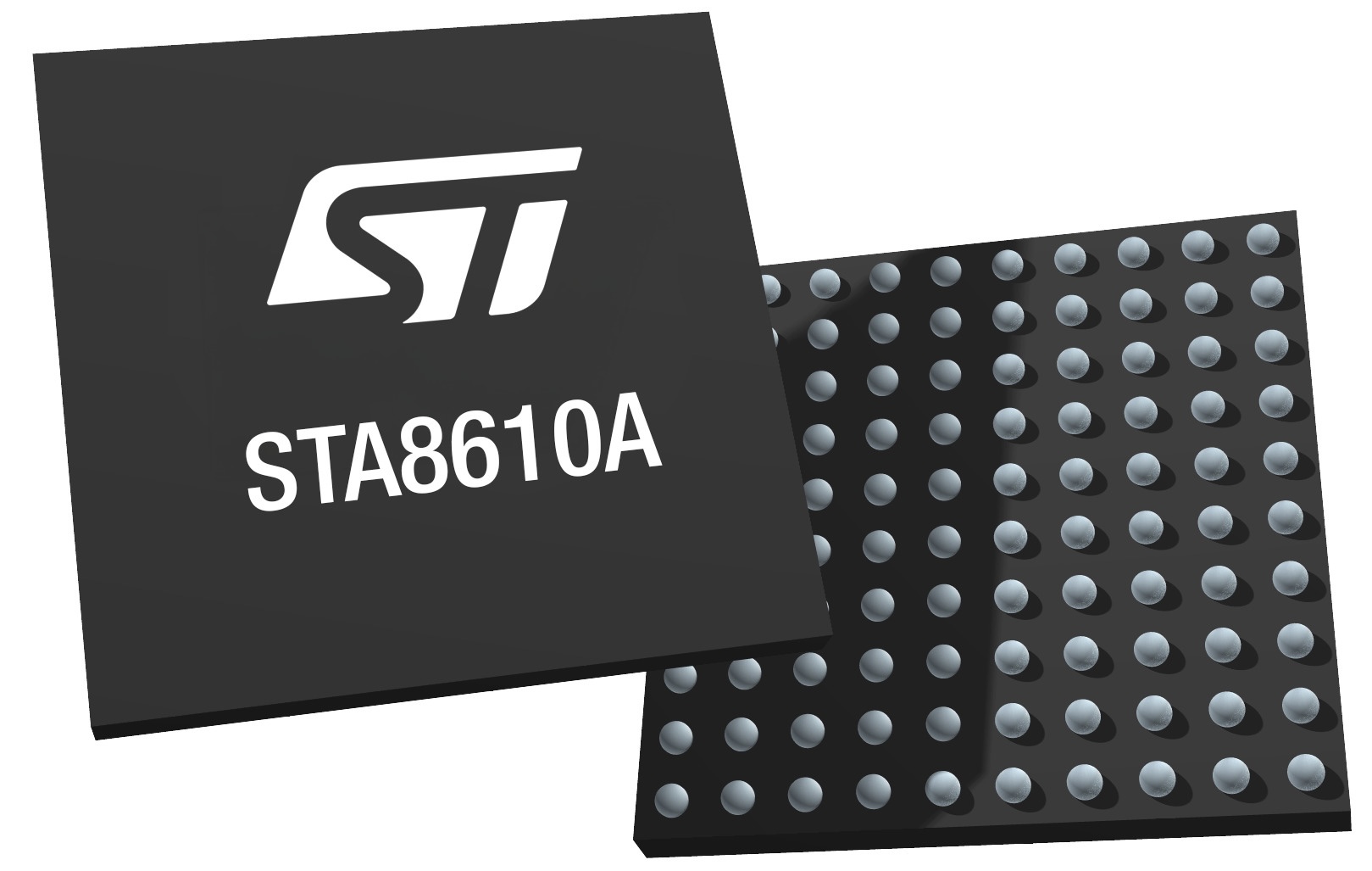 TeseoVI+ (STA8610A)
The new TeseoVI also supports the open service navigation message authentication (OSNMA) from the Galileo constellation. In a nutshell, the feature prevents spoofing attacks by cryptographically authenticating the source of a message. Very simply, the technology uses a message authentication code (MAC) to guarantee the authenticity of a signal’s provenance. It doesn’t encrypt the whole message but sends a series of codes, which is a far more efficient use of the bandwidth. Consequently, since Galileo generates the code, hackers can’t fake it. Additionally, since the standard sends multiple codes over time, hackers can’t just grab one key and reuse it in a replay attack. By the time they do so, the key has expired.
How to support OSNMA?To support OSNMA, hardware manufacturers must update their firmware and their software stack and offer enough processing power to handle the extra computations. This is why ST also provides extensive software implementations with its GNSS receivers. We know that taking advantage of new features can be complex. In this instance, decoding the OSNMA fields and managing the keys requires complex libraries that must pass audits and receive regular updates. Hence, the TeseoVI not only supports this anti-spoofing technology but enables developers to take advantage of it in their applications rapidly.
Making multiband more accessible More advanced features to mainstream cars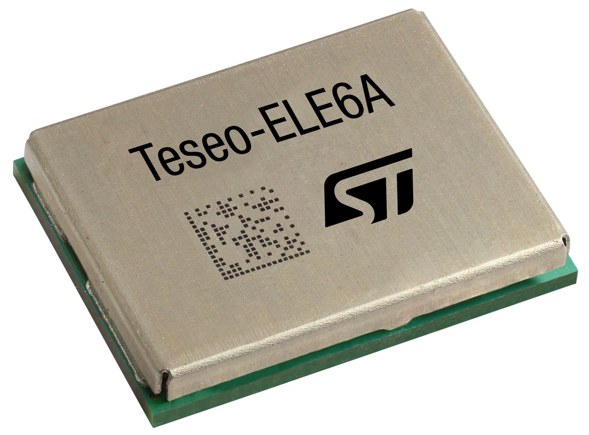 Teseo-ELE6A
One of the greatest benefits of a single-die design is the ability to lower the cost of materials. In fact, since there’s no need for external RF and external memory, engineers may target a BOM cost of about a dollar. Obviously, this is only a general reference point. In practice, the price will vary based on the complexity of the design and volumes. However, in all cases, it means that previous customers who used to avoid multiband solutions because they were too expensive will now be able to jump on the bandwagon. For instance, we can expect level 2 and 3 autonomous driving features to reach more mainstream vehicles.
More flexibility to integrators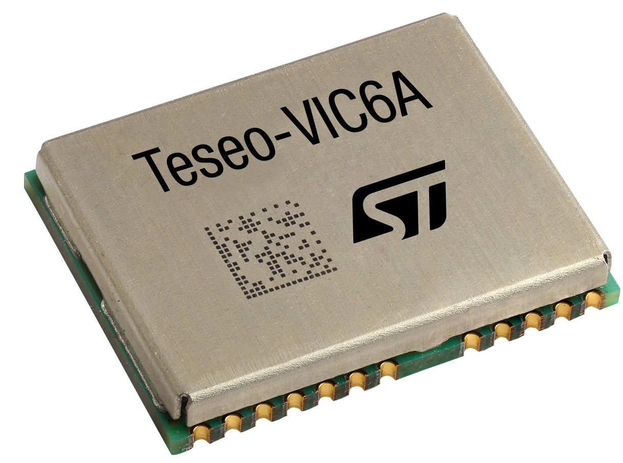 Teseo-VIC6A
The TeseoVI is also the first GNSS receiver for automotives to have a pin-to-pin compatible version for safety applications, the TeseoAPP2 (STA9200MA), which features the same QFN56 package as the TeseoVI (STA8600A). As a result, developers can simply create one reference design and switch between the ASIL-certified and the non-certified part number, depending on their needs.
ST will also be offering the TeseoVI+ (STA8610A). It’s the same device as the TeseoVI, but the TeseoVI+ can welcome custom algorithms thanks to dual M7 Core Processing and External Memory Interface (Flash/RAM). Hence, teams wanting to use their application can do away with our positioning and measurement software. Finally, we also offer a module with a 6-axis inertial sensor, the Teseo-VIC6A, and its safety alter ego, the Teseo-ELE6A.
The post TeseoVI: ST’s 1st single-die quad-band GNSS receiver makes autonomous driving mainstream appeared first on ELE Times.
Renesas Partners with Indian Government to Drive Innovation Through Startups and Industry-Academia Collaboration, Strengthening India’s Semiconductor Ecosystem
MOUs Signed with Indian Government and Inauguration of Renesas’ Bengaluru and Noida Offices Mark Investments to Accelerate Growth in India’s Key Semiconductor Hubs
Renesas Electronics Corporation announced its partnership with the Ministry of Electronics & Information Technology (MeitY), Government of India, to support local startups and academic institutions in the field of VLSI and embedded semiconductor systems. Renesas also celebrated the expansion of its offices in Bengaluru and Noida to accommodate its growing R&D teams, with the inauguration ceremonies. This strategic move underscores Renesas’ commitment to innovation and excellence in India and aims to drive continued growth in the region.
Renesas and the Centre for Development of Advanced Computing, an autonomous scientific society of MeitY, today signed and exchanged two Memoranda of Understanding (MOUs) under the MeitY Chips to Startup. These MOUs focus on 1) Supporting local startups by enabling them to drive technological advancement and promote local manufacturing in alignment with the Make in India initiative; and 2) Enhancing industry-academia collaboration by fostering an innovative, product-focused mindset among students.
India is a key market for Renesas, offering significant growth potential and access to a highly skilled talent pool. Recent collaborations include the OSAT factory project with CG power and Stars Microelectronics in Gujarat and the MOU with IIT Hyderabad. Renesas is also expanding its operations in India, with plans to increase its headcount to 1,000 by the end of 2025. This growth initiative reinforces Renesas’ long-term commitment to India and supports its ambition to become an employer of choice in this dynamic and fast-evolving market.
“The inauguration of our expanded offices marks a significant milestone for Renesas in India. It reflects our unwavering commitment to innovation, excellence, and the nurturing of local talent. By building products in India, for India and the world, we continue to drive growth and deliver meaningful impact across the Indian market,” said Malini Narayanamoorthi, India Country Manager and VP, MID Engineering, Analog & Connectivity Group at Renesas. “We are proud to sign two MOUs under the MeitY C2S programme, focused on advancing research, fostering innovation, and nurturing product-focused engineers. These strategic collaborations align with the Make in India initiative, aiming to strengthen local design and manufacturing capabilities and empower homegrown talent to drive the future of industry.”
MOUs under MeitY C2S programme
Renesas and C-DAC signed two MOUs to collaborate in the field of VLSI and embedded semiconductor systems, with the aim of supporting local startups and academic institutions to accelerate innovation and foster self-reliance in India’s semiconductor and product ecosystem. The C2S programme encompasses collaboration with over 250 academic institutions and R&D organizations across the country, including IITs, NITs, IIITs, government and private colleges, along with approximately 15 startups, creating a strong ecosystem for indigenous innovation.
- MOU for Startups: Renesas will help strengthen the product engineering capabilities of local startups by providing Renesas development boards and Altium Designer,the leading PCB design software.
- MOU for Academic Institutions: Renesas will support experiential learning by offering development boards, PCB education and training, Altium Designer software, and access to the Altium 365 cloud platform, aiming to empower the next generation of electronics engineers and nurture a community of innovators.
The post Renesas Partners with Indian Government to Drive Innovation Through Startups and Industry-Academia Collaboration, Strengthening India’s Semiconductor Ecosystem appeared first on ELE Times.
PSOC 4100T Plus microcontroller offers advanced sensing capabilities and system control in a single chip
Infineon Technologies AG introduces PSOC 4100T Plus, an Arm Cortex-M0+ microcontroller (MCU) with Multi-Sense. The new microcontroller offers a rich blend of analog and digital capabilities, featuring 128K Flash, 32K SRAM, and Infineon’s high-performance Multi-Sense technology, which includes CAPSENSE, inductive sensing and liquid level sensing. PSOC 4100T Plus also boasts enhanced reliability and is equipped with a range of enhancements and advanced sensing capabilities to form a complete solution for system control and human-machine interface applications.
“Infineon is committed to delivering best-in-class system control and HMI solutions with enhanced reliability,” says Vibheesh Bharathan, Director and Project Lead for PSOC 4 Multi-Sense from Infineon. “Our Multi-Sense capability represents a paradigm shift, driving next-generation sensing solutions for HMI and system control use cases. In this way, we are enabling the digitalization solutions of tomorrow for consumer and industrial applications.”
PSOC 4100T Plus can be used as a standalone general-purpose microcontroller, providing a robust platform for system control and management OR it can be utilized as a specialized HMI MCU, enabling the creation of intuitive and interactive interfaces. Alternatively, PSOC 4100T Plus can serve a single chip solution for both system control and touch HMI.
In its HMI MCU configuration, the device supports a range of sensing applications, including capacitive sensing for detecting user touch or proximity, inductive sensing for enabling touch over metallic surfaces, Machine Learning based liquid level sensing for monitoring liquid presence or levels, and CAPSENSE-based hover touch for detecting finger touch through a large airgap, making it a powerful tool for creating innovative and user-friendly interfaces.
PSOC 4100T Plus is a versatile and powerful platform designed to support a broad range of applications. For example:
Home appliances: Reliability is the top priority for home appliances. The PSOC 4100T Plus series addresses this critical requirement with significant enhancements, including 6500 V best-in-class electrostatic discharge protection and a 1% internal main oscillator accuracy. In addition, the advanced HMI features, such as hover touch, provide a solution to several design challenges, including the need for simplified and cost-effective stack up, touch operation through airgap. With the combination of complementary sensing technologies of Multi-Sense, designers can effectively address the design challenges they face.
Consumer electronics: PSOC 4100T Plus series elevates the human-machine interface capabilities in consumer electronics by providing a compact and efficient solution for sensor designs. Leveraging its 5th Generation CAPSENSE technology, the PSOC 4100T Plus offers high signal-to-noise ratio and low power consumption. Additionally, its waterproof design enables the device to operate reliably in harsh environments, including outdoor applications.
Touchpad and touchscreen applications: PSOC 4100T Plus series offers a high resolution 2D finger tracking user interface, enabling the creation touchpads and touchscreens. With 32 sensor inputs, the device can be configured to support up to 256 nodes, allowing for a wide range of design possibilities. For example, a touchpad can be designed with an 80mm x 80mm surface area with a 5mm diamond pitch, resulting in a high-resolution multi-finger tracking. Similarly, a 4-inch touchscreen can be driven by PSOC 4100T Plus for multi-finger use. Both touchpad and touchscreen user interfaces supported with built-in, configurable gesture engine.
To support the development of multi-sense applications, a comprehensive suite of software tools and resources are offered. The CAPSENSE Tuner allows designers to easily configure and optimize capacitive sensing applications, while the Inductive Sensing Design Guide and Liquid Level Sensing Design Guide provide detailed guidance on implementing these technologies. Additionally, the ML-based liquid level sensing model trainer enables developers to overcome challenges like manufacturing variations, varying airgaps with removable tanks.
The post PSOC 4100T Plus microcontroller offers advanced sensing capabilities and system control in a single chip appeared first on ELE Times.
2nd Year Engineering Student - Final Project for my Solid State Electronics 2 Class
 | This is my final semester at community college. I wil be attending a 4 year university this fall, as a junior, to finish off my bachelor's in electrical engineering. My final project is an analog function generator. It is capable of generating a sine wave, triangle wave, and a square wave. It is based on an online project called "Analog Function Generator" by "laserjocky". The circuit consists of op-amps, resistors, capacitors, transistors, potentiometers, and switches. The images are of the initial wave created by a specific op-amp and the final wave generated at the final output. [link] [comments] |
Midsummer receives US$14.8m order for CIGS PV production line
Luminus launches CFT-50X Series LED product line for medical, life sciences and industrial applications
IC verification tool addresses design complexity, productivity gap

A new software combines connectivity, scalability and data-driven artificial intelligence (AI) capabilities to push the boundaries of the IC verification process and make chip design teams more productive. Questa One aims to address the verification productivity gap for large, complex designs spanning IP to IC to systems.
The steadily increasing complexity of 3DICs, chiplet-based designs, and software-defined architectures is further compounded by a critical talent shortage and growing demands for enhanced security and lower power consumption. “Questa One uses new technical advances to deliver the fastest functional, fault, and formal verification engines available,” said Abhi Kolpekwar, VP and GM of digital verification technologies at Siemens EDA.

Figure 1 Questa One strives to redefine IC verification from a reactive process into an intelligent, self-optimizing system. Source: Siemens EDA
A recent Wilson Research Group survey suggests that one in seven IC projects achieves first-time silicon success. Chris Giles, director of product management for static and formal at Siemens EDA, calls this a jaw-dropping and staggering drop. “Our approach is to enable engineers to do more with less, with not just faster engines but also faster engineers with fewer workloads,” he said.

Figure 2 Here is a view of the decline in first-time silicon success and the increase in FPGA bugs. Source: Wilson Research Group
Giles spoke with EDN to explain the technology fundamentals of this new verification tool.
Quest One’s three tenets
Giles said that Questa One has been developed around three core principles:
- Scalable verification: It allows engineers to speed verification closure. Giles noted that the semiconductor industry is struggling to tackle large designs. “That’s why we see a decline in first-time silicon success,” he added. “Chip designs are getting so large that it’s difficult to verify them in one piece.” Questa One verification aims to allow engineers to work on large chip designs.
- Data-driven verification: It leverages data for AI-powered analytics to bring new insights and to improve verification productivity. “It collects datasets that allow verification tools to either make recommendations or directly decide what to do next and do it productively,” said Giles.
- Connected verification: Questa One connects EDA tools and verification IP to form a cohesive ecosystem for robust verification, validation, and test operations. In other words, it uses a broad set of technologies and analyses to provide insights and raw verification power.

Figure 3: Questa One offerings are shown with three main value propositions summed up at the bottom. Source: Siemens EDA
Quest One’s four components
Questa One has the following focus areas:
- Questa One simulator: This simulator engine is built from the ground up. It performs functional and fault simulation for RTL, GLS, and DFT applications with parallel processing and profiling add-ons.
- Questa One SFV: The stimulus-free verification (SFV) solution delivers user productivity through synergistic combinations of static and formal analyses, AI, automation, and parallelization. “The current static and formal technology is very fragmented, challenging high productivity,” Giles said. “SFV integrates static and formal analyses, AI, and parallelization to address this challenge.”
- Questa One verification IQ: It’s a coverage solution that utilizes generative, analytic, and prescriptive AI to drive verification closure faster with fewer workloads. “It features an intelligent interface that provides insight into the entire verification ecosystem,” Giles added.
- Questa One Avery VIP: The solution, based on Avery’s high-quality VIP and high-coverage compliance test suites (CTS), offers protocol-aware debug and coverage analytics to help increase productivity. It supports 3DIC and chiplet verification from IP to system-on-chip (SoC) design.

Figure 4 Four main components of Questa One include a simulator, a static and formal verification solution, a verification intelligence coverage analysis solution, and an Avery identifier. Siemens EDA
Questa One in works
Semiconductor IP supplier Rambus acknowledged an improved verification experience in managing data center workloads like generative AI while implementing IPs for PCIe, CXL, and HBM interfaces. Rambus particularly mentioned Questa One’s simulation, static and formal analysis, and verification IP technologies.
Then there is Arm, which used Questa One simulator to reduce regression time in its latest AArch64 architecture. “The Questa One verification solution has improved our verification productivity across traditional on-premises and cloud deployments,” said Karima Dridi, head of productivity engineering at Arm.
MediaTek, another early user of Questa One, has utilized its formal verification and simulation technologies. “Questa One Property Assist utilizes generative AI to save us weeks of engineering time, and Questa One Regression Navigator predicts which simulation tests are most likely to fail, runs them first, and saves days of regression and debugging time,” said Chienlin Huang, senior technical manager of Connectivity Technology Department at MediaTek.
Questa One claims to yield step-function gains in smart regression, smart analysis, smart engine, and smart debug domains. Design testimonials from Arm, MediaTek, and Rambus are a good start.
Related Content
- How Do You Verify IC Performance?
- Integrate tools for effective verification
- The profile of a data-driven IC design verification tool
- Why verification matters in network-on-chip (NoC) design
- IC design: A short primer on the formal methods-based verification
The post IC verification tool addresses design complexity, productivity gap appeared first on EDN.
На ФЕЛ вдосконалюють електрохірургічні установки

Понад 20 років тому українські науковці – інженери, медики, фізики, біологи – під керівництвом академіка Б.Є. Патона розробили та впровадили технологію зварювання живих м'яких тканин.
A simple circuit to let you characterize JFETs more accurately

In April 2012, EDN published a circuit by John Fattaruso that lets you quickly measure the drain-source saturation current and the pinch-off voltage of both an N-JFET and a P-JFET. The pinch-off voltage (Vp) is measured by inserting a very large resistance between the source and the ground. The drain-source saturation current (IDSS) is measured by inserting a small resistance between the source and the ground. Then, the voltage across this resistor is measured, and both Vp and IDSS can be calculated using Ohm’s law.
There is a catch with this circuit: Since IDSS is measured across a non-zero resistor, there is a deviation from the real IDSS, see Figure 1. This circuit does not really measure point A, but actually measures point B slightly before this. For JFETs with lower Vp voltages and/or higher IDSS currents, there can be a deviation between the measured and real IDSS value of 5% or more.

Figure 1 A standard N-JFET drain-source current vs gate-source voltage curve.
Wow the engineering world with your unique design: Design Ideas Submission Guide
Circuit ideaThe accuracy of the circuit can be drastically increased by making a couple of minor changes. Figure 2 shows the basic circuit.

Figure 2 A basic, improved circuit for the JFET IDSS and Vp measurement.
An astute reader will immediately see the two circuits’ similarities and differences. Switch 1 is, again, used to select between N-channel JFETs and their less common sibling: P-channel JFETs.
Switch 2 is used to select between Vp and IDSS measurement. In the position as drawn, IDSS is measured. In this position, A1 is set up as a transimpedance amplifier.
With the op-amp’s non-inverting input connected to ground, A1 will keep the inverting input, and hence the source, to ground as well. This guarantees that the true IDSS is measured. Resistor R3 then converts the current to a voltage that can be measured at the output of A1.
When Switch 2 is flipped to the other position, A1 is set up as a simple voltage follower. The pinch-off voltage that develops across R1 is then buffered and available at the output of A1.
Full implementationNow that we have seen the basic circuit, we can look at a full implementation (Figure 3). Resistor R2 limits the current that can flow in case a JFET is inserted incorrectly. In pinch-off measurement mode, the impedances around Q1, R1 and A1 are all pretty high. To limit the influence of noise, capacitor C1 is added. It is best to keep these wires short and/or to build the circuit in a shielded box.

Figure 3 First implementation of the practical circuit used to measure IDSS and Vp.
Most operational amplifiers can only source or sink a small amount of current. The drain-source saturation current can easily be in the tens of milliamperes. To boost the current output capabilities of A1, a complementary bipolar transistor output stage is added. Please note that the output is not short-circuit proof. If preferred, a simple 1 kΩ to 10 kΩ resistor can be added in series with the output.
With the current resistor values in the circuit, a pinch-off voltage of ±10 V can be measured and a saturation current of ~ ±100 mA.
Although there are JFETs with large saturation currents (think J109 with IDSS > 40 mA and J108 with IDSS > 80 mA!), this is simply not needed for most JFETs. So, a variation on this circuit was developed. The pinch-off voltage remained the same, but the saturation current was returned to 25 mA, covering almost all JFET types. A further requirement was that the output voltage range for both measurements needed to be the same: 0 … ±5 V. This was so that a moving coil meter readout could be used with a single range.
See Figure 4 for the implementation.

Figure 4 A circuit with the tailored measurement range that is suited for most JFETs.
Read-outA read-out needs to be added to make this a complete measurement instrument. Since I have a large stock of moving coil meters, I decided to use one of these for the read-out. To some, they may look antiquated, but they are a joy to use and a marvel of mechanical engineering! The output can be positive or negative depending on whether you are measuring Vp or IDSS, and whether an N-type JFET or a P-type JFET is being tested. So, this is something that needs to be dealt with. Also, it would be nice if there were some kind of polarity indication. See Figure 5 for the read-out circuit.

Figure 5 The readout circuit with sensitive polarity indication.
The 1-mA moving coil meter is included in the feedback loop around the op-amp. D3-D6 form a common rectifier bridge so that, independent of the polarity of the input voltage, the meter is always fed a positive current.
Transistors Q1 and Q2 serve as a polarity indication. Positive voltages will turn on Q1 and LED D9. LED D10 will indicate negative voltages.
D7,8 are not needed for the rectification. Because of these diodes, the A1 output voltage must be above/below ±1.8 V before any significant current will flow through the meter. This, in turn, guarantees that transistors Q1 and Q2 will already turn on at very low input voltages, giving a good polarity indication across the whole input range.
Test socketOver the years, manufacturers have created JFETs with almost every possible pin-out, so making a single universal test socket is not so trivial. With three leads, there are 3! = 6 possible combinations as shown in Table 1.
|
# |
Pin-out |
||
|
1 |
G |
D |
S |
|
2 |
G |
S |
D |
|
3 |
D |
G |
S |
|
4 |
D |
S |
G |
|
5 |
S |
G |
D |
|
6 |
S |
D |
G |
Table 1 The six possible pin-out combinations that can be used for an off-the-shelf JFET.
Of course, a JFET with a pin-out of S-D-G (#6) can be tested in a socket with pin-out G-D-S (#1), simply by inserting it reverse in the socket. This effectively eliminates half of the possible combinations. So we are left with the following three, as shown in Table 2.
|
# |
Pin-out |
||
|
1 |
G |
D |
S |
|
2 |
G |
S |
D |
|
3 |
D |
G |
S |
|
4 |
= #2 reverse |
||
|
5 |
= #3 reverse |
||
|
6 |
= #1 reverse |
||
Table 2 A reduction in the number of pin-out combinations by simply reversing the component within the test socket.
After a bit of doodling, we can create a single five-pin test socket that can accommodate every possible JFET pin-out as shown in Table 3.
|
# |
Pin-out |
||||
|
D |
S |
G |
D |
S |
|
Table 3 A singular 5-pin test socket to accommodate all possible JFET pin-outs.
There are two different variants possible; this is left as an exercise to the reader. The same logic can be applied to create universal test sockets for bipolar transistors, of course.

Figure 6 The final PCB implementation of the practical JFET circuit used to measure IDSS and Vp, showing the test socket.
In closingThanks to John Fattaruso for his excellent design idea, which sprouted this idea! We all stand on the shoulders of the giants that came before us.
Cor van Rij blew his first fuse at 10 under the close supervision of his father, who promptly forbade him from ever working on the house mains again. He built his first regenerative receiver at the age of 12, and as a boy, his bedroom was decorated with all sorts of antennas, and a huge collection of disassembled radios took up every horizontal surface. He studied electronics and graduated cum laude.
He worked as a data design engineer and engineering manager in the telecom industry. And has worked for almost 20 years as a principal electrical design engineer, specializing in analog and RF electronics and embedded firmware. Every day is a new discovery!
Related Content
- Simple circuit lets you characterize JFETs
- A Conversation with Mike Engelhardt on QSPICE
- Your friend, the JFET.
- Building a JFET voltage-tuned Wien bridge oscillator
The post A simple circuit to let you characterize JFETs more accurately appeared first on EDN.
Науковці КПІ отримали фінансування від МОН

Понад 650 проєктів фундаментальних та прикладних наукових досліджень, виконавцями яких є заклади вищої освіти й наукові установи, що належать до сфери управління Міністерства освіти і науки України, було подано на конкурс МОН. Після завершення експертиз та оцінювання в секціях, затверджено перелік із-понад 130 проєктів-переможців, які пройшли конкурсний відбір та фінансування яких розпочнеться цього року за кошти Державного бюджету України. Серед них і 8 проєктів, які будуть виконуватися в КПІ ім. Ігоря Сікорського впродовж найближчих трьох років.
Australian National Fabrication Facility orders Riber MBE 412 cluster platform
NUBURU files $100m SEC registration statement to enhance capital flexibility
Infineon introduces CoolGaN Bidirectional Switch 650 V G5 for enhanced efficiency and reliability in power systems
Infineon Technologies AG is introducing the CoolGaN Bidirectional Switch 650 V G5, a gallium nitride (GaN) switch capable of actively blocking voltage and current in both directions. Featuring a common-drain design and a double-gate structure, it leverages Infineon’s robust gate injection transistor technology to deliver a monolithic bidirectional switch, enabled by Infineon’s CoolGaN technology. The device serves as a highly efficient replacement for traditional back-to-back configurations commonly used in converters.
The bidirectional CoolGaN switch offers several key advantages for power conversion systems. By integrating two switches in a single device, it simplifies the design of cycloconverter topologies, enabling single-stage power conversion, eliminating the need for multiple conversion stages. This leads to improved efficiency, increased reliability, and a more compact design. BDS-based microinverters also benefit from higher power density and reduced component count, which simplifies manufacturing and reduces costs. Additionally, the device supports advanced grid functions such as reactive power compensation and bidirectional operation.
As a result, this solution holds significant potential across a wide range of applications, including:
Microinverters: The CoolGaN bidirectional switch enables simpler and more efficient microinverter designs, reducing both size and cost. This makes microinverters more attractive for residential and commercial solar installations.
Energy Storage Systems (ESS): In ESS applications such as battery chargers and dischargers, the switch allows for more efficient and reliable energy storage and release.
Electric Vehicle (EV) Charging: In EV charging systems, the BDS switch supports faster, more efficient charging while also enabling vehicle-to-grid functionality, where energy stored in the vehicle battery can be fed back into the grid.
Motor control: The CoolGaN BDS is ideal for use in Current Source Inverters for industrial motor drives. Compared to traditional Voltage Source Inverters, CSIs offer benefits such as:
- Producing a sinusoidal output voltage, which supports longer cable runs, reduced losses, and improved fault tolerance.
- Replacing the DC-link capacitor with an inductor, improving high-temperature performance and short-circuit protection.
- Higher efficiency at partial loads, lower EMI, inherent buck-boost capability for voltage variation, and scalability for parallel operation.
These features make CSIs a more robust and efficient alternative for industrial motor applications.
AI data centers: In AI server power supplies, bidirectional switches like CoolGaN support higher switching frequencies and power density in architectures such as Vienna rectifiers and H4 PFCs. A single CoolGaN BDS can replace two conventional switches, reducing component count, cost, size, and overall power losses.
The post Infineon introduces CoolGaN Bidirectional Switch 650 V G5 for enhanced efficiency and reliability in power systems appeared first on ELE Times.
Top 10 RAM Brands in India
Random Access Memory (RAM) is an essential part of any computing system, its speed and efficiency depending on it. India’s RAM market has seen strong growth over the past few years due to growing demand for high-end computing, gaming and enterprise applications. The Indian RAM market has both local and foreign players, providing a variety of RAM modules such as DDR3, DDR4, and DDR5 technologies. In India, there are quite a few brands that provide top-notch RAM modules for various purposes. Here’s a glimpse at the top 10 RAM brands in India, their origin and specifications.
- Corsair
Corsair is one of the first memory module makers based in the United States that primarily serves as a supplier for gamers, business users and PC enthusiasts, Its RAM is designed with aggressive cooling systems, customizable RGB color, and optimum speed for overlocking.
- Kingston
Kingston, an American company, specializes in the manufacturing of top-class memory solutions. It provides dependable RAM modules under various categories such as DDR3, DDR4, and DDR5, along with its HyperX line that caters to gamers and high-end users.
- Samsung
Samsung, headquartered in South Korea, is a world leader in semiconductor technology and producers top-notch RAM modules. Their memory solutions offer superior speed and efficiency and are in great demand for use in laptops, desktops and workstations. The company manufactures memory solutions over a range of generations, such as DDR3, DDR4 and DDR5, which find applications in various devices, from laptops and desktops to enterprise servers.
- G. SKILL
Based in Taiwan, G. SKILL is a leader in gaming memory solutions, offering ultra-high -speed frequencies and leading cooling technology. Their Trident Z series RAM modules are especially well-linked among gaming enthusiasts searching for extreme overlocking capabilities.
- Crucial
A Micron subsidiary, Crucial is U.S. based and offers reliable and cost-effective RAM solutions. Its Ballistix series popularized, Crucial RAM has widespread use for general computing while being both performant and price -effective.
- ADATA
Taiwanese by origin, ADATA produces high-speed RAM modules featuring innovative designs. ADATA produces DDR4 and DDR5 memory solutions, with the XPG gaming series being specifically designed for gamers looking for top-class performance and longevity.
- Transcend
Another Taiwanese company, Transcend is known for making industrial-grade memory modules. RAM solutions by Transcend are designed for long-lasting durability and can be used in commercial and consumer applications.
- SK Hynix
Headquartered in South Korea, SK Hynix is an expert in enterprise-level memory solutions. Their RAM products guarantee high-speed performance, reliability and peak efficiency, serving professional and industrial computing purposes.
- Patriot
Patriot, an American company, specializes in providing high-performance RAM solutions with superior heat dissipation technology. Their Viper gaming line is designed for gaming systems that need fast and stable memory.
10. TeamGroup
Located in Taiwan, TeamGroup specializes in manufacturing stylish and high-performance RAM modules. Their T-Force gaming line offers a blend of appearance and superior cooling technology, and hence it is a top pick for users who are into performance.
|
Brand Name |
Example Model |
Key Specifications |
|
Corsair |
Corsair Vengeance RGB Pro | DDR4, DDR5, RGB options, High-speed modules |
|
Kingston |
Kingston Fury Beast |
DDR3, DDR4, DDR5, Value and HyperX series |
|
G. SKILL |
G. SKILL Trident Z RGB |
DDR4, DDR5, High-frequency modules, RGB lighting |
|
Crucial |
Crucial Ballistix |
DDR3, DDR4, DDR5, Low-cost alternatives |
|
ADATA |
ADATA XPG Spectrix D60G |
DDR3, DDR4. DDR5, XPG Gaming series |
|
Transcend |
Transcend Jet Ram |
DDR3, DDR4, DDR5, Industrial-grade memory |
|
Samsung |
Samsung DDR4-3200 |
DDR3, DDR4, DDR5, High-capacity modules |
|
Hynix |
SK Hynix Gold P31 |
DDR3, DDR4, DDR5, Enterprise-grade memory |
|
Patriot |
Patriot Viper Steel |
DDR4, DDR5, Viper gaming series |
| TeamGroup | TeamGroup T-Force Delta |
RGB, DDR4, DDR5, T-Force gaming series |
There is competition among brands in the varied Indian RAM market to offer dependable, fast memory solutions for a range of computing requirements. While Transcend, ADATA, and Crucial provide good mid-range options, Corsair, Kingston, and G. SKILL stand out as premium options for gaming and high-performance applications. With their commitment to quality and innovation, Samsung and Hynix remain formidable competitors in the semiconductor sector.
The post Top 10 RAM Brands in India appeared first on ELE Times.
Серія семінарів «Аспекти національної безпеки та оборони»

🇺🇦🇺🇸 У межах третього із серії семінарів «Аспекти національної безпеки та оборони» до нашого університету завітали визнані авторитети у сфері військової аналітики — контрадмірал ВМС США Марк Монтгомері та генерал-майор ВПС США Чарльз Коркоран.
Infineon and Visteon Collaborate on Advanced Power Conversion Systems for Next-Generation Electric Vehicles
Infineon Technologies AG, the leading provider of automotive semiconductors, and Visteon Corporation, a global leader in automotive cockpit electronics, announced the companies have signed a Memorandum of Understanding to advance the development of next-generation electric vehicle powertrains.
In this joint effort, Infineon and Visteon will collaborate and integrate power conversion devices based on Infineon semiconductors, with particular emphasis on wideband gap device technologies, which provide significant advantages in power conversion applications compared to silicon-based semiconductors. These devices include greater power density, efficiency and thermal performance, which contribute to improved efficiency and reduced system costs for next-generation power conversion modules for the automotive sector.
Future Visteon EV powertrain applications incorporating Infineon CoolGaN (Gallium Nitride) and CoolSiC (Silicon Carbide) devices may include battery junction boxes, DC-DC converters and on-board chargers. The resulting powertrain systems will conform to the highest efficiency, robustness and reliability.
“Working with Infineon allows us to integrate cutting-edge semiconductor technologies that are essential in improving power conversion efficiency and overall system capability of next generation electric vehicles,” said Dr. Tao Wang, Head of the Electrification Product Line of Visteon Corporation. “This collaboration will advance technologies that accelerate the transition to a more sustainable and efficient mobility ecosystem.”
“Visteon is a recognized innovator and an early adopter of new technologies, making them an ideal partner for us,” said Peter Schaefer, Chief Sales Officer Automotive, Infineon Technologies AG. “Together, we will push the boundaries of electric vehicle technology and provide superior solutions to the global automotive industry.”
The post Infineon and Visteon Collaborate on Advanced Power Conversion Systems for Next-Generation Electric Vehicles appeared first on ELE Times.
G2-57 Soviet hardware true RNG
 | Here's a new interesting addition to my collection of Soviet equipment - the G2-57 hardware true RNG. Didn't expect it to be so packed inside, but I guess you need a lot of circuitry to provide basically anything you'd want from an RNG. This device outputs: 1. Binary random signal with adjustable amplitude and bit width, with ability to generate endless random signal or repeating random patterns of up to 21 bits. 2. Analog random signal with gaussian distribution and adjustable frequency range. 3. Analog random signal with continuous uniform distribution and adjustable frequency range. [link] [comments] |
Infineon introduces CoolGaN bidirectional switch 650V G5
Silicon carbide substrate revenue falls 9% to $1.04bn in 2024, says TrendForce
Pages

