
Feed aggregator
Fixed a flaky toaster oven button.
 | This button has been working intermittently. I pulled it out and noticed it was less "clicky" than the others. Had spares on a scrap board. Works perfectly now. The hardest part was getting into that area of the toaster. [link] [comments] |
Developing high-performance compute and storage systems

Peripheral Component Interconnect Express, or PCI Express (PCIe), is a widely used bus interconnect interface, found in servers and, increasingly, as a storage and GPU interconnect solution. The first version of PCIe was introduced in 2003 by the Peripheral Component Interconnect Special Interest Group (PCI-SIG) as PCIe Gen 1.1. It was created to replace the original parallel communications bus, PCI.
With PCI, data is transmitted at the same time across many wires. The host and all connected devices share the same signals for communication; thus, multiple devices share a common set of address, data, and control lines and clearly vie for the same bandwidth.
With PCIe, however, communication is serial point-to-point, with data being sent over dedicated lines to devices, enabling bigger bandwidths and faster data transfer. Signals are transferred over connection pairs, known as lanes—one for transmitting data, the other for receiving it. Most systems normally use 16 lanes, but PCIe is scalable, allowing up to 64 lanes or more in a system.
The PCIe standard continues to evolve, doubling the data transfer rate per generation. The latest is PCIe Gen 7, with 128 GT/s per lane in each direction, meeting the needs of data-intensive applications such as hyperscale data centers, high-performance computing (HPC), AI/ML, and cloud computing.
PCIe clockingAnother differentiating factor between PCI and PCIe is the clocking. PCI uses LVCMOS clocks, whereas PCIe uses differential high-speed current-steering logic (HCSL) and low-power HCSL clocks. These are configured with the spread-spectrum clocking (SSC) scheme.
SSC works by spreading the clock signal across several frequencies rather than concentrating it at a single peak frequency. This eliminates large electromagnetic spikes at specific frequencies that could cause interference (EMI) to other components. The spreading over several frequencies reduces EMI, which protects signal integrity.
On the flip side, SSC introduces jitter (timing variations in the clock signal) due to frequency-modulating the clock signal in this scheme. To preserve signal integrity, PCIe devices are permitted a degree of jitter.
In PCIe systems, there’s a reference clock (REFCLK), typically a 100-MHz HCSL clock, as a common timing reference for all devices on the bus. In the SSC scheme, the REFCLK signal is modulated with a low-frequency (30- to 33-kHz) sinusoidal signal.
To best balance design performance, complexity, and cost, but also to ensure best functionality, different PCIe clocking architectures are used. These are common clock (CC), common clock with spread (CCS), separate reference clock with no spread (SRNS), and separate reference clock with independent spread (SRIS). Both CC and separate reference architectures can use SSC but with a differing amount of modulation (for the spread).
Each clocking scheme has its own advantages and disadvantages when it comes to jitter and transmission complexity. The CC is the simplest and cheapest option to use in designs. Here, both the transmitter and receiver share the same REFCLK and are clocked by the same PLL, which multiplies the REFCLK frequency to create the high-speed clock signals needed for the data transmission. With the separate clocking scheme, each PCIe endpoint and root complex have their own independent clock source.
PCIe switchesTo manage the data traffic on the lanes between different components within a system, PCIe switches are used. They allow multiple PCIe devices, from network and storage cards to graphics and sound cards, to communicate with one another and the CPU simultaneously, optimizing system performance. In cloud computing and AI data centers, PCIe switches connect multiple NICs, GPUs, CPUs, NPUs, and other processors in the servers, all of which require a robust and improved PCIe infrastructure.
PCIe switches play a key role in next-generation open, hyperscale data center specifications now being worked on rapidly by a growing developer contingent around the world. This is particularly needed with the advent of ML- and AI-centric data centers, underpinned by HPC systems. PCIe switches are also instrumental in many industrial setups, wired networking, communications systems, and where many high-speed devices must be connected with data traffic managed effectively.
A well-known brand of PCIe switches is the Switchtec family from Microchip Technology. The Switchtec PCIe switch IP manages the data flow and peer-to-peer transfers between ports, providing flexibility, scalability, and configurability in connecting multiple devices.
The Switchtec Gen 5.0 PCIe high-performance product lineup delivers very low system latency, as well as advanced diagnostics and debugging tools for troubleshooting and fast product development, making it highly suitable for next-generation data center, ML, automotive, communications, defense, and industrial applications, as well as other sectors. Tier 1 data center providers are relying on Switchtec PCIe switches to enable highly flexible compute and storage rack architectures.
Reference design and evaluation kit for PCIe switchesTo enable rapid, PCIe-based system development, Microchip has created a validation board reference design, shown in Figure 1, using the Switchtec Gen 5 PCIe Switch Evaluation Kit, known as the PM52100-KIT.
 Figure 1: Microchip’s Switchtec Gen 5 PCIe switch reference design validation board (Source: Microchip Technology Inc.)
The reference design helps developers implement the Switchtec Gen 5 PCIe switch into their own systems. The guidelines show designers how to connect and configure the switch and how to reach the best balance for signal integrity and power, as well as meet other critical design aspects of their application.
Fully tested and validated, the reference design streamlines development and speeds time to market. The solution optimizes performance, costs, and board footprint and reduces design risk, enabling fast market entry with a finished product. See the solutions diagram in Figure 2.
 Figure 2: Switchtec Gen 5 PCIe solutions setup with other key devices (Source: Microchip Technology Inc.)
As with all Switchtec PCIe switch designs, full access to the Microchip ChipLink diagnostics tool is included, which allows parameter configuration, functional debug, and signal integrity analysis.
As per all PCIe integrations, clock and timing are important aspects of the design. Clock solutions must be highly reliable for demanding end applications, and the Microchip reference design includes complete PCIe Gen 1–5 timing solutions that include the clock generators, buffers, oscillators, and crystals.
Microchip’s ClockWorks Configurator and product selection tool allow easy customization of the timing devices for any application. The tool is used to configure oscillators and clock generators with specific frequencies, among other parameters, for use within the reference design.
The Microchip PM52100-KITFor firsthand experience of the Switchtec Gen 5 PCIe switch, Microchip provides the PM52100-KIT (Figure 3), a physical board with 52 ports. The kit enables users to experiment with and evaluate the Switchtec family of Gen 5 PCIe switches in real-life projects. The kit was built with the guidance provided by the Microchip reference design.
 Figure 3: The Microchip PM52100-KIT (Source: Microchip Technology Inc.)
The kit contains an evaluation board with the necessary firmware and cables. Users can download the ChipLink diagnostic tool by requesting access via a myMicrochip account.
With the ChipLink GUI, which is suitable for Windows, Mac, or Linux systems, the board’s hardware functions can easily be accessed and system status information monitored. It also allows access to the registers in the PCIe switch and configuration of the high-speed analog settings for signal integrity evaluation. The ChipLink diagnostic tool features advanced debug capabilities that will simplify overall system development.
The kit operates with a PCIe host and supports the connection of multiple host entities to multiple endpoint devices.
The PCIe interface contains an edge connector for linking to the host, several PCIe Amphenol Mini Cool Edge I/O connectors to connect the host to endpoints, and connectors for add-in cards. The 0.60-mm Amphenol connector allows high-speed signals to Gen 6 PCIe and 64G PAM4/PCIe, but also Gen 5 and Gen 4 PCIe. This connector maintains signal integrity, as its design minimizes signal loss and reflections at higher frequencies.
The board’s PCIe clock interface consists of a common reference clock (with or without SSC), SRNS, and SRIS. A single stable clock, with low jitter, is shared by both endpoints. The second most common clocking scheme is SRNS, where an independent clock is supplied to each end of the PCIe link; this is also supported by the Microchip kit.
Among the kit’s peripherals are two-wire (TWI)/SMBus interfaces; TWI bus access and connectivity to the temperature sensor, fan controller, voltage monitor, GPIO, and TWI expanders; SEEPROM for storage and PCIe switch configuration; and 100 M/GE Ethernet. The kit also includes GPIOs for TWI, SPI, SGPIO, Ethernet, and UART interfaces. There is UART access with a USB Type-B and three-pin connector header.
The included PSX Software Development Kit (integrating GHS’s MULTI development environment) enables the development and testing of the custom PCIe switch functionalities. An EJTAG debugger supports test and debug of custom PSX firmware; a 14-pin EJTAG connector header allows PSX probe connectivity.
Switchtec Gen 5 52-lane PCIe switch reference designMicrochip also offers a Switchtec 52-lane Gen 5 PCIe Switch Reference Design (Figure 4). As with the other reference design, it is fully validated and tested, and it provides the components and tools necessary to thoroughly assess and integrate this design into your systems.
This board includes a 32-bit microcontroller (ATSAME54, based on the Arm Cortex-M4 processor with a floating-point unit) to be configured with Microchip’s MPLAB Harmony software, as well as a CEC1736 root-of-trust controller. The CEC1736 is a 96-MHz Arm Cortex-M4F controller that is used to detect and provide protection for the PCIe system against failure or malicious attacks.
 Figure 4: Switchtec Gen 5 52-lane PCIe switch reference design board (Source: Microchip Technology Inc.)
Microchip and the PCIe standard
Figure 4: Switchtec Gen 5 52-lane PCIe switch reference design board (Source: Microchip Technology Inc.)
Microchip and the PCIe standard
Microchip continues to be actively involved in the advancement of the PCIe standard, and it regularly participates in PCI-SIG compliance and interoperability events. With its turnkey PCIe reference designs and field-proven interoperable solutions, a high-performance design can be streamlined and brought to market very quickly.
To view the full details of this reference design, bill of materials, and to download the design files, visit https://www.microchip.com/en-us/tools-resources/reference-designs/switchtec-gen-5-pcie-switch-reference-design.
The post Developing high-performance compute and storage systems appeared first on EDN.
A digital filter system (DFS), Part 2

Editor’s note: In this Design Idea (DI), contributor Bonicatto designs a digital filter system (DFS). This is a benchtop filtering system that can apply various filter types to an incoming signal. The filtering range is up to 120 kHz.
In Part 1 of this DI, the DFS’s function and hardware implementation are discussed.
In Part 2 of this DI, the DFS’s firmware and performance are discussed.
FirmwareThe firmware, although a bit large, is not too complicated. It is broken into six files to make browsing the code a bit easier. Let’s start with the code for the LCD screen, and its attached touch detector.
Wow the engineering world with your unique design: Design Ideas Submission Guide
LCD and touchscreen codeHere might be a good place to show the LCD screens, as they will be discussed below.
 The LCD screen in the DFS. From the top left: Splash Screen, Main Screen, Filter Selection Screen, Cutoff or Center Frequency Screen, Digital Gain Screen, About Screen, and Running Screen.
A quick discussion of the screens will give you a good overview of the operation and capabilities of the DFS. The first screen is the opening or Splash Screen—not much here to see, but there is a battery charge icon on the upper right.
Touching this screen anywhere will move you to the Main Screen. The Main Screen shows you the current settings and allows you to jump to the appropriate screen to adjust the filter type, cutoff, or center frequency of the filter, and the digital gain. It also has the “RUN” button that starts the filtering function based on the current settings.
If you touch the “Change Filter Type” on the Main Screen, you will jump to the Filter Selection Screen. This lets you select the filter type you would like to use and if you want 2-pole or 4-pole filtering. (Selecting a 2-pole filter will give you a roll-off of 24 dB per octave or 80 dB per decade, while the 4-pole will provide you with a roll-off of 12 dB per octave or 40 dB per decade.) When you touch the “APPLY” button, your settings (in green) will be applied to your filter, and you will jump back to the Main Screen.
In the Main Screen, if you want to change the cutoff/center frequency. You can set any frequency up to 120 kHz. Hitting “Enter” will bring you back to the Main Screen.
If you want to change the digital gain (gain applied when the filter is run on a sample, between the ADC and the DAC, touch “Change Output Gain” on the Main Screen. The range for this gain is from 0.01 to 100. Again, “Enter” will take you back to the Main Screen.
On the Main Screen, selecting “About” will take you to a screen showing lots of interesting information, such as your filter settings, your current filter’s coefficients, battery voltage, and charge level. (If you do not have a battery installed, you may see fully charged numbers as it is seeing the charger voltage. There is a #define at the top of the main code you can set to false if you don’t have a battery installed, and this line won’t show.) The last item shown is the incoming USB voltage.
In the main code, hitting “Run” will start the system to take in your signal at the input BNC, filter it, and send it out the output BNC. The Running Screen also shows you the current filter settings.
Now, let’s take a quick look at the mechanics of creating the screens. The LCD uses a few libraries to assist in the display of primitive shapes and colors, text, and to provide some functions for reading the selected touchscreen position. When opening the Arduino code, you will find a file labeled “TFT_for_adjustable_filter_7.ino”. This file contains the code for most of the screen displays and touchscreen functions. The code is too long to list here, but here are a few lines of code setting the background color and displaying the letters “DFS”:
tft.fillScreen(tft.color565(0xe0, 0xe0, 0xe0)); // Grey tft.setFont(&FreeSansBoldOblique50pt7b); tft.setTextColor(ILI9341_RED); tft.setTextSize(1); tft.setCursor(13, 100); tft.print("DFS");A lot of the functions look like this, as they are used to present the data and create the keypads for filter selection, frequency setting, and digital gain setting. In this file are also the functions for monitoring and logically connecting the touch to the appropriate function.
The touchscreen, although included on the LCD, is essentially independent from it. One issue that needed to be solved was that the alignment of the touchscreen over the LCD screen is not accurate, and pixel (0,0) is not aligned with the touch position (0,0) on the touchscreen.
Also, the LCD has 240×320 pixels, and the touch screen has, roughly, 3900×900 positions. So there needs to be some calibration and then a conversion function to convert the touch point to the LCD’s pixel coordinates. You’ll see in the code that, after calibration, the conversion function is very easy using the Arduino map() function.
Other filesThere is also a file that contains the initialization code for the ADC. This sets up the sample rate, resolution, and other needed items. Note that this is run at the start of the code, but also when changing the number of poles in the filter. This is due to the need to change the sample rate. Another file contains the code to initialize the DAC, and is also called when the program is started.
Also included is a file with code to pull in factory calibration data for linearizing the ADC. This calibration data is created at the factory and is stored in the microcontroller (micro)—nice feature.
Filtering codeNow to the more interesting code. There is code to route you to the screens and their selections, but let’s skip that and look at how the filtering is accomplished. After you have selected a filter type (low-pass, high-pass, band-pass, or band-stop), the number of poles of the filter (2 or 4), the cutoff or center frequency of the filter, or adjusted the internal digital output gain, the code to calculate the Butterworth IIR filter coefficients is called.
These coefficients are calculated for a direct form II filter algorithm. The coefficients for the filters are floats, which allow the system to create filters accurately throughout a 1 Hz to 120 kHz range. After the coefficients are calculated, the filter can be run. When you touch the “RUN” button, the code begins the execution of the filter.
The first thing that happens in the filter routine is that the ADC is started in a free-running mode. That means it initiates a new ADC reading, waits for the reading to complete, signals (through a register bit) that there is a new reading available, and then starts the cycle again. So, the code must monitor this register bit, and when it is set, the code must quickly get the new ADC reading and filter it, and then send that filtered value to the DAC for output.
After this, it checks for clipping in the ADC or DAC. The input to the DFS is AC-coupled. Then, when it enters the analog front-end (AFE), it is recentered at about 1.65 V. If any ADC sample gets too close to 0 or too close to 4095 (it’s a 12-bit ADC), it is flagged as clipping, and the front panel input clipping LED will light for ~ 0.5 seconds. This could happen if the input signal is too large or the input gain dial has been turned up too far.
Similarly, the DAC output is checked to see if it gets too close to 0 or to 2047 (we’ll explain why the DAC is 11 bits in a moment). If it is, it is flagged as clipping, and the output clipping LED will light for ~0.5 seconds. Clipping of the DAC could happen because the digital gain has been set too high. Note that the output signal could be set too high, using the output gain dial, and it could be clipping the signal, but this would not be detected as the amplified analog back-end (ABE) signal is not monitored in the micro.
Now to why the DAC is 11 bits. In the micro, it is actually a 12-bit DAC, but in an effort to get the sample rate as fast as possible, I discovered that the DAC had an unspec’d slew rate limit of somewhere around 1 volt/microsecond.
To work around this, I divide the signal being passed to the DAC by two so the DAC’s output voltage doesn’t have to slew so far. This is compensated for in the ABE as the actual gain of the output gain adjust is actually 2 to 10, but represented as 1 to 5. [To those of you who are questioning why I didn’t set the reference to 1.65 (instead of 3.3 V) and use the full 12 bits, the answer is this micro has a couple of issues on its analog reference system that precluded using 1.65 V.]
One last task in the filter “running” loop is to check if the “Stop” has been pressed. This a simple input bit read so it only takes few cycles.
A couple of notes on filtering: You may have noticed that there is an extra filter you can select – the “Pass-Thru”. This takes in the ADC reading, “filters” it by only multiplying the sample by the selected digital gain. It then outputs it to the DAC. I find this useful for checking the system and setup.
Another note on filtering is that you will see, in the code, that a gain offset is added when filtering. The reason for this is that, when using a high-pass or band-pass filter, the DC level is removed from the samples. We need to recenter the result at around 2048 counts. But we can’t just add 2048, as the digital gain also comes into play. You’ll see this compensation calculated using the gain and applied in the filtering routines.
PerformanceI managed to get the ADC and DAC to work at 923,645 samples per second (sps) when using any of the 2-pole filters. This is a Nyquist frequency around 462 kHz. Since the selectable upper rate for a filter is 120 kHz, we get an oversample rate of almost 4. For 4-pole filters, the system runs at 795,250 sps, for an oversample rate of around 3.3.
The 4-pole filters are slower as they are created by cascading two 2-pole filters. [To check these sample rates and see if the loop has enough time to complete before the following sample is read, I toggle the D4 digital output as I pass through the loop. I then monitor this on a scope.]
The noise floor of the output signal is fairly good, but as I built this on a protoboard with no ground planes, I think it could be lower if this were built on a PCB with a good ground plane. The limiting factor on my particular board, though, is the spurious free dynamic range (SFDR).
I do get harmonic spurs at various frequencies, but I can get up to a 63 dB SFDR. This is not far from the SFDR spec of the ADC. I did notice that the amplitude of these harmonic spurs changed when I moved cables inside the enclosure, so good cable management may improve this.
Use of AIRecently, I’ve been using AI in design, and I like to include quick information describing if AI helped in the design—here’s how it worked out. The code to initialize the ADC was quite difficult, mostly because there was a lot of misinformation about this online.
I used Microsoft Copilot and ChatGPT to assist. Both fell victim to some of the online misinformation, but by pointing out some of the errors, I got these AI systems close enough that I could complete the ADC initialization myself.
To design the battery charge indicator on the splash screen, I used the same AI. It was a pure waste of time as it produced something that didn’t look like a battery – it was easier and faster to design it myself.
The code for the filter coefficients was difficult to track down online, and ChatGPT did a much better job of searching than Google.
For circuit design, I tried to use AI for the Sallen-Key filter designs, but it was a failure, just a waste of time. Stick to the IC supplier tools for filter design.
Tried to use AI to design a nice splash screen, but I wasted more time iterating with the chatbot than it took to design the screen.
I also tried to get AI to design an enclosure with a viewable LCD, BNC connectors, etc. To be honest, I didn’t give it a lot of chances, but it couldn’t get it to stop focusing on a flat rectangular box.
ModificationsThe code is actually easy to read, and you may want to modify it to add features (like a circular buffer sample delay) or modify things like the filter coefficient calculations. I think you’ll find this DFS has a number of uses in your lab/shop.
The schematic, code, 3D print files, links to various parts, and more information and notes on the design and construction can be downloaded at: https://makerworld.com/en/@user_1242957023/upload
Damian Bonicatto is a consulting engineer with decades of experience in embedded hardware, firmware, and system design. He holds over 30 patents.
Phoenix Bonicatto is a freelance writer.
Related Content
- A digital filter system (DFS), Part 1
- How much help are free AI tools for electronic design?
- Non-linear digital filters: Use cases and sample code
- A beginner’s guide to power of IQ data and beauty of negative frequencies – Part 1
- A Sallen-Key low-pass filter design toolkit
- Designing second order Sallen-Key low pass filters with minimal sensitivity to component tolerances
- Toward better behaved Sallen-Key low pass filters
- Design second- and third-order Sallen-Key filters with one op amp
The post A digital filter system (DFS), Part 2 appeared first on EDN.
Open World Foundation Models Generate Synthetic Worlds for Physical AI Development
Courtesy: Nvidia
Physical AI Models- which power robots, autonomous vehicles, and other intelligent machines — must be safe, generalized for dynamic scenarios, and capable of perceiving, reasoning and operating in real time. Unlike large language models that can be trained on massive datasets from the internet, physical AI models must learn from data grounded in the real world.
However, collecting sufficient data that covers this wide variety of scenarios in the real world is incredibly difficult and, in some cases, dangerous. Physically based synthetic data generation offers a key way to address this gap.
NVIDIA recently released updates to NVIDIA Cosmos open-world foundation models (WFMs) to accelerate data generation for testing and validating physical AI models. Using NVIDIA Omniverse libraries and Cosmos, developers can generate physically based synthetic data at incredible scale.
Cosmos Predict 2.5 now unifies three separate models — Text2World, Image2World, and Video2World — into a single lightweight architecture that generates consistent, controllable multicamera video worlds from a single image, video, or prompt.
Cosmos Transfer 2.5 enables high-fidelity, spatially controlled world-to-world style transfer to amplify data variation. Developers can add new weather, lighting and terrain conditions to their simulated environments across multiple cameras. Cosmos Transfer 2.5 is 3.5x smaller than its predecessor, delivering faster performance with improved prompt alignment and physics accuracy.
These WFMs can be integrated into synthetic data pipelines running in the NVIDIA Isaac Sim open-source robotics simulation framework, built on the NVIDIA Omniverse platform, to generate photorealistic videos that reduce the simulation-to-real gap. Developers can reference a four-part pipeline for synthetic data generation:
- NVIDIA Omniverse NuRec neural reconstruction libraries for reconstructing a digital twin of a real-world environment in OpenUSD, starting with just a smartphone.
- SimReady assets to populate a digital twin with physically accurate 3D models.
- The MobilityGen workflow in Isaac Sim to generate synthetic data.
- NVIDIA Cosmos for augmenting generated data.
From Simulation to the Real World
Leading robotics and AI companies are already using these technologies to accelerate physical AI development.
Skild AI, which builds general-purpose robot brains, is using Cosmos Transfer to augment existing data with new variations for testing and validating robotics policies trained in NVIDIA Isaac Lab.
Skild AI uses Isaac Lab to create scalable simulation environments where its robots can train across embodiments and applications. By combining Isaac Lab robotics simulation capabilities with Cosmos’ synthetic data generation, Skild AI can train robot brains across diverse conditions without the time and cost constraints of real-world data collection.
Serve Robotics uses synthetic data generated from thousands of simulated scenarios in NVIDIA Isaac Sim. The synthetic data is then used in conjunction with real data to train physical AI models. The company has built one of the largest autonomous robot fleets operating in public spaces and has completed over 100,000 last-mile meal deliveries across urban areas. Serve’s robots collect 1 million miles of data monthly, including nearly 170 billion image-lidar samples, which are used in simulation to further improve robot models.
See How Developers Are Using Synthetic Data
Lightwheel, a simulation-first robotics solution provider, is helping companies bridge the simulation-to-real gap with SimReady assets and large-scale synthetic datasets. With high-quality synthetic data and simulation environments built on OpenUSD, Lightwheel’s approach helps ensure robots trained in simulation perform effectively in real-world scenarios, from factory floors to homes.
Data scientist and Omniverse community member Santiago Villa is using synthetic data with Omniverse libraries and Blender software to improve mining operations by identifying large boulders that halt operations.
Undetected boulders entering crushers can cause delays of seven minutes or more per incident, costing mines up to $650,000 annually in lost production. Using Omniverse to generate thousands of automatically annotated synthetic images across varied lighting and weather conditions dramatically reduces training costs while enabling mining companies to improve boulder detection systems and avoid equipment downtime.
FS Studio partnered with a global logistics leader to improve AI-driven package detection by creating thousands of photorealistic package variations in different lighting conditions using Omniverse libraries like Replicator. The synthetic dataset dramatically improved object detection accuracy and reduced false positives, delivering measurable gains in throughput speed and system performance across the customer’s logistics network.

Robots for Humanity built a full simulation environment in Isaac Sim for an oil and gas client using Omniverse libraries to generate synthetic data, including depth, segmentation and RGB images, while collecting joint and motion data from the Unitree G1 robot through teleoperation.

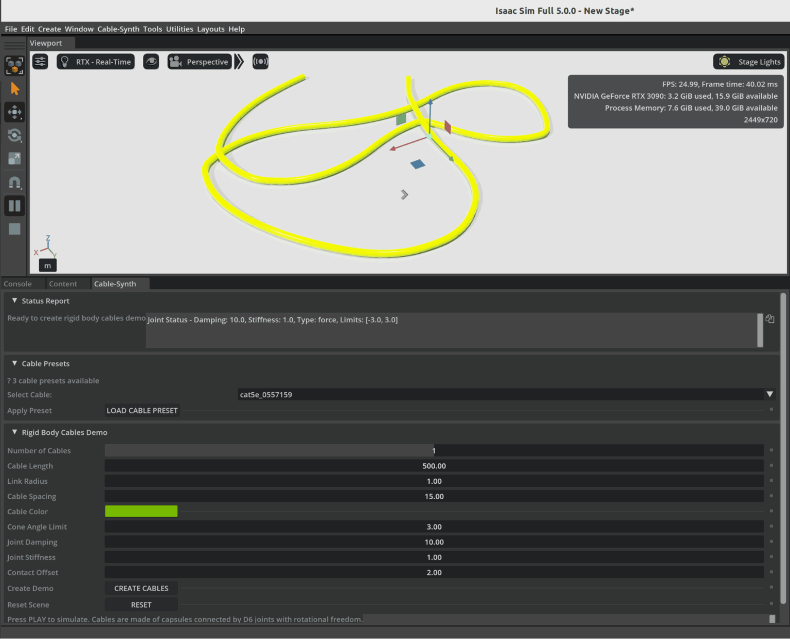
Omniverse Ambassador Scott Dempsey is developing a synthetic data generation synthesizer that builds various cables from real-world manufacturer specifications, using Isaac Sim to generate synthetic data augmented with Cosmos Transfer to create photorealistic training datasets for applications that detect and handle cables.
Conclusion
As physical AI systems continue to move from controlled labs into the complexity of the real world, the need for vast, diverse, and accurate training data has never been greater. Physically based synthetic worlds—driven by open-world foundation models and high-fidelity simulation platforms like Omniverse—offer a powerful solution to this challenge. They allow developers to safely explore edge cases, scale data generation to unprecedented levels, and accelerate the validation of robots and autonomous machines destined for dynamic, unpredictable environments.
The examples from industry leaders show that this shift is already well underway. Synthetic data is strengthening robotics policies, improving perception systems, and drastically reducing the gap between simulation and real-world performance. As tools like Cosmos, Isaac Sim, and OpenUSD-driven pipelines mature, the creation of rich virtual worlds will become as essential to physical AI development as datasets and GPUs have been for digital AI.
In many ways, we are witnessing the emergence of a new engineering paradigm—one where intelligent machines learn first in virtual environments grounded in real physics, and only then step confidently into the physical world. The Omniverse is not just a place to simulate; it is becoming the training ground for the next generation of autonomous systems.
The post Open World Foundation Models Generate Synthetic Worlds for Physical AI Development appeared first on ELE Times.
Ascent Solar closes up to $5.5m private placement
Космічний шлях одесита Георгія Добровольського

Наша газета вже писала про те, як відзначали цьогорічний Всесвітній тиждень космосу в Державному політехнічному музеї ім. Бориса Патона. Серед заходів програми була й лекція, присвячена пам'яті уродженця України, космонавта Георгія Добровольського – піонера тривалих пілотованих космічних польотів і командира екіпажу космічного корабля "Союз-11".
How Well Will the Automotive Industry Adopt the Use of AI for its Manufacturing Process
Gartner believes that by 2029, only 5% of automakers will maintain strong AI investment growth, a decline from over 95% today.
“The automotive sector is currently experiencing a period of AI euphoria, where many companies want to achieve disruptive value even before building strong AI foundations,” said Pedro Pacheco, VP Analyst at Gartner. “This euphoria will eventually turn into disappointment as these organizations are not able to achieve the ambitious goals they set for AI.”
Gartner predicts that only a handful of automotive companies will maintain ambitious AI initiatives after the next five years. Organizations with strong software foundations, tech-savvy leadership, and a consistent very long-term focus on AI will pull ahead from the rest, creating a competitive AI divide.
“Software and data are the cornerstones of AI,” said Pacheco. “Companies with advanced maturity in these areas have a natural head start. In addition, automotive companies led by execs with strong tech know-how are more likely to make AI their top priority instead of sticking to the traditional priorities of an automotive company.”
Fully-Automated Vehicle Assembly Predicted by 2030
The automotive industry is also heading for radical operational efficiency. As automakers rapidly integrate advanced robotics into their assembly lines, Gartner predicts that by 2030, at least one automaker will achieve fully automated vehicle assembly, marking a historic shift in the automotive sector.
“The race toward full automation is accelerating, with nearly half of the world’s top automakers (12 out of 25) already piloting advanced robotics in their factories,” said Marco Sandrone, VP Analyst at Gartner. “Automated vehicle assembly helps automakers reduce labor costs, improve quality, and shorten production cycle times. For consumers, this means better vehicles at potentially lower prices.”
While it may reduce the direct need for human labor in vehicle assembly, new roles in AI oversight, robotics maintenance and software development could offset losses if reskilling programs are prioritized.
The post How Well Will the Automotive Industry Adopt the Use of AI for its Manufacturing Process appeared first on ELE Times.
Electronics manufacturing and exports grow manifold in the last 11 years
Central government-led schemes, including PLI for large-scale electronics manufacturing (LSEM) and PLI for IT hardware, have boosted both manufacturing and exports in the broader electronics category and the mobile phone segment.
The mobile manufacturing in India has taken a tremendous rise. In last 11 years, total number of mobile manufacturing units have increased from 2 to more than 300. Since the launch of PLI for LSEM, Mobile manufacturing has increased from 2.2 Lakh Cr in 2020-21 to 5.5 Lakh Cr.
Minister of State for Electronics and Information Technology Jitin Prasada, in a question, informed Rajya Sabha on Friday that as a result of policy efforts, electronics manufacturing has grown almost six times in the last 11 years – from ₹1.9 lakh crore in 2014-15 to ₹11.32 lakh crore in 2024-25.
The booming industry has generated employment for approximately 25 lakh people and the electronic exports have grown by eight times since 2014-15.
According to the information submitted by Union Minister for Electronics and Information Technology Shri Ashwini Vaishnaw in Rajya Sabha, to encourage India’s young engineers, the Government is providing latest design tools to 394 universities and start-ups. Using these tools, chip designers from more than 46 universities have designed and fabricated the chips using these tools at Semiconductor Labs, Mohali.
Also, all major semiconductor design companies have set up design centers in India. Most advanced chips such as 2 nm chips are now being designed in India by Indian designers.
The post Electronics manufacturing and exports grow manifold in the last 11 years appeared first on ELE Times.
A quick primer demystifies parabolic microphones

Parabolic microphones offer a fascinating blend of geometry and acoustics, enabling long-distance sound capture with surprising clarity. From dish-shaped reflectors to pinpoint audio focus, this quick primer distills the essentials for engineers and curious minds exploring high-gain directional solutions.
Parabolic microphones are specialized tools designed to capture sounds that are too faint for conventional microphones, or when precise directional focus is essential. By concentrating acoustic energy from a narrow field, a well-designed parabolic microphone can isolate a single sound source amid a noisy environment. These microphones are commonly used in nature recording, sports broadcasting, surveillance, and even drone detection.
Understanding parabolic microphones
Capturing audio for sound reinforcement, broadcast television, live performances, video production, or natural ambience requires choosing the right microphone for the job. Ideally, the sound source should be positioned close to the microphone to maximize signal strength and minimize interference from ambient noise or the microphone’s own self-noise. A signal-to-noise ratio (SNR) in the range of 40–60 dB is typically desirable. For distant or low-level sound sources, microphone’s self-noise should be especially low—below 10 dBA is recommended.
In applications like sporting events, surveillance and nature sound recording, getting close to the source is often impractical. Only a well-designed parabolic microphone can deliver suitable SNR under these conditions. Keep in mind that audio signal level drops by 6 dB every time the distance to the source is doubled, and the farther you are, the more unwanted ambient sounds creep in.
Parabolic microphones address both challenges by combining a narrow polar angle with high forward gain. Much like a telephoto camera lens, a parabolic dish offers greater magnification at long distances—but with a tighter field of view.
At the central focal point of a portable parabolic dish, incoming sound waves converge with remarkable intensity. The concept of using a parabolic (semi-spherical) reflector to capture distant sounds has been around for decades, and with good reason.
Unlike conventional microphones, a parabolic reflector acts as a noiseless acoustic amplifier—boosting signal strength without adding electronic noise. Its frequency response and polar pattern are directly influenced by the size of the dish, with larger reflectors offering narrower pickup angles and extended low-frequency reach.
As shown below, the operating principle of a parabolic microphone is straightforward to visualize. Incoming sound waves reflect off the curved surface of the dish and converge at its focal point, where the microphone element captures and converts them into audio signals with enhanced directionality and gain.

Figure 1 A conceptual diagram of a parabolic microphone demonstrates its acoustic focusing mechanism and focal point geometry. Source: Author
Simply put, a parabolic dish collects sound energy from a broad area and concentrates it onto a single focal point, where a microphone is positioned. By focusing acoustic energy in this way, the dish acts as a mechanical amplifier, boosting signal strength without introducing electronic noise. This passive amplification enables the microphone to capture faint or distant sounds with greater clarity, making the system ideal for applications where electronic gain alone would be insufficient or too noisy.
As an aside, although the parabolic dish is designed to reflect sound waves toward its focal point, not all waves strike the microphone diaphragm at the same angle. For this reason, omnidirectional microphones are typically used; they maintain consistent sensitivity regardless of the direction of incoming sound.
This may seem counterintuitive at first: the parabolic system is highly directional, yet it employs an omnidirectional microphone. The key is that the dish provides directionality, while the mic simply needs to capture all focused energy arriving at the focal point.
Parabolic microphones: Buy or DIY?
A complete parabolic microphone system typically includes one or more microphone elements, a parabolic reflector, a mounting mechanism to position the microphone at the dish’s focal point, an optional preamplifier or headphone amplifier, and a way to handhold the assembly or mount it on a tripod.
If you are looking to acquire such a system, you have three main paths: you can purchase a fully assembled unit that includes the microphone element and, optionally, built-in amplification; you can opt for a nearly complete setup that provides the dish and mounting hardware but leaves the microphone and electronics up to you; or you can build your own from scratch, sourcing each component to suit your specific needs.
A parabolic microphone makes an excellent DIY project for several compelling reasons. The underlying principles are fascinating yet easy to grasp, and construction is not prohibitively complex. More than just a science experiment, the finished system can be genuinely useful—whether for nature recording, surveillance, or acoustic research.
Material costs are typically far lower than those of comparable commercial units, making DIY both practical and rewarding. For that reason, the next section highlights a few key design pointers to help you build your own parabolic microphone.
In addition to the all-important dish diameter, three other factors play a critical role when selecting a reflector for a parabolic microphone: the dish’s focal-length-to-diameter (f/D) ratio, the precision of its parabolic curvature, and the smoothness of its inner surface. Each of these influences how effectively the dish focuses sound and how cleanly the microphone captures it.
Oh, this is just a personal suggestion, but I strongly recommend buying a professionally molded parabolic dish rather than attempting to make one from scratch. The reflector is the most critical part of the system, and its precision directly affects performance.
A quick pick is the plastic parabolic dish from Wildtronics, which offers reliable geometry and build quality for DIY use. My purpose in writing this note is not to endorse any particular parabolic dish, but simply to offer a practical pointer that may help others construct a working parabolic microphone with minimal frustration and cost.

Figure 2 The polycarbonate parabolic reflector is engineered for sound amplification. Source: Wildtronics
Once you have a reliable dish, the rest of the build becomes far more manageable. You can then add mechanical accessories such as mic mounts, handles, tripod brackets, and a suitable windshield to reduce wind noise and protect the microphone.
Vital components like an electret microphone element and supporting audio electronics—whether a simple preamplifier or a full recording interface—complete the setup. With the dish as your foundation, assembling a functional and effective parabolic microphone becomes a rewarding DIY process.
Acoustic sensor for DIY parabolic mic
To wrap up, here is a proven acoustic sensor design for a DIY parabolic microphone, built around the Primo EM272 electret condenser microphone.

Figure 3 Basic schematic of an acoustic sensor for a parabolic mic that is built around the Primo EM272 ECM. Source: Author
In an earlier prototype, I used a slightly tweaked prewired monaural audio amplifier module to process signals from this stage, and it performed exactly as expected.
Enjoyed this quick dive into parabolic microphones? With just enough theory to anchor the fundamentals and a few practice-ready tips to spark experimentation, this post is only the beginning. Whether you are a field recordist, audio tinkerer, or simply acoustically curious, there is more to explore.
Read the full post, and if it strikes a chord, I will value your perspective. Every signal adds clarity.
 T.K. Hareendran is a self-taught electronics enthusiast with a strong passion for innovative circuit design and hands-on technology. He develops both experimental and practical electronic projects, documenting and sharing his work to support fellow tinkerers and learners. Beyond the workbench, he dedicates time to technical writing and hardware evaluations to contribute meaningfully to the maker community.
Related Content
- Acoustic Design for MEMS Microphones
- MEMS Microphones Busting Out All Over
- Microphones: An abundance of options for capturing tones
- Analog and digital MEMS microphone design considerations
- Designer’s guide: picking the right MEMS microphone for voice-control applications
The post A quick primer demystifies parabolic microphones appeared first on EDN.
Taiwanese company to invest 1,000 crore in Karnataka for new electronics & semiconductor park
Allegiance Group signed a Memorandum of Understanding (MoU) with Karnataka to develop an India-Taiwan Industrial Park, creating a dedicated hub for advanced electronics and semiconductor manufacturing.
Karnataka has secured a major foreign investment with Taiwan-based Allegiance Group signing an MoU to establish a ₹1,000-crore India-Taiwan Industrial Park (ITIP) focused on electronics and semiconductor manufacturing. The agreement was signed by IT/BT director Rahul Sharanappa Sankanur and Allegiance Group vice president Lawrence Chen.
Chief Minister Siddaramaiah welcomed the investment, stating that the project will bring cutting-edge technologies to the state and enhance India’s role in the global electronics value chain.
The proposed ITIP will be developed as a dedicated zone for Taiwanese companies specialising in advanced manufacturing, R&D, and innovation. According to the state government, the park is expected to generate 800 direct jobs over the next five years and will strengthen Karnataka’s position in high-value manufacturing.
This investment comes as Karnataka intensifies efforts to expand its manufacturing footprint. Just last week, American firm Praxair India announced plans to invest ₹200 crore in its operations in the state over the next three years.
The Allegiance Group, which recently committed ₹2,400 crore for similar industrial facilities in Andhra Pradesh and Telangana, said the Bengaluru project would act as a strong catalyst for Taiwanese companies entering the Indian market. “The ITIP will help Taiwanese firms scale in India and support the growth of the semiconductor and electronics ecosystem,” said Lawrence Chen.
IT/BT minister Priyank Kharge stated that the facility will deepen India-Taiwan business ties and strengthen collaboration in emerging technologies. The project aims to build a full supply chain ecosystem, including components, PCBs, and chip design, while also encouraging technology transfer and global best practices.
Industries minister M.B. Patil noted that Karnataka has signed over 115 MoUs worth ₹6.57 lakh crore in the last two years, and continues to attract leading global manufacturers such as Tata Motors, HAL, and Bosch.
The post Taiwanese company to invest 1,000 crore in Karnataka for new electronics & semiconductor park appeared first on ELE Times.
The 2025 MRAM Global Innovation Forum will Showcase MRAM Technology Innovations, Advances, & Research from Industry Experts
The MRAM Global Innovation Forum is the industry’s premier platform for Magnetoresistive Random Access Memory (MRAM) technology, bringing together leading magnetics experts and researchers from industry and academia to share the latest MRAM advancements. Now in its 13th year, the annual one-day conference will be held the day after the IEEE International Electron Devices Meeting (IEDM) on December 11, 2025 from 8:45am to 6pm at the Hilton San Francisco Union Square Hotel’s Imperial Ballroom A/B.
The 2025 MRAM technical program includes 12 invited presentations from leading global MRAM experts, as well as an evening panel. The programs will throw light on technology development, product development, tooling and other exploratory topics.
MRAM technology, a type of non-volatile memory is known for its high speed, endurance, scalability, low power consumption and radiation hardness. Data in MRAM devices is stored by magnetic storage elements instead of an electric charge, in contrast to conventional memory technologies. MRAM technology is increasingly used in embedded memory applications for automotive microcontrollers, edge AI devices, data centers, sensors, aerospace, and in wearable devices.
“The STT-MRAM market is growing rapidly now, especially with use of embedded STT-MRAM in next-generation automotive microcontroller units,” said Kevin Garello, MRAM Forum co-chair (since 2021) and senior researcher engineer at SPINTEC. “I expect edge AI applications to be the next big market for STT-MRAM.”
“I am pleased to see that over the years, the MRAM Forum series has grown into a landmark event within the MRAM industrial ecosystem,” said Bernard Dieny, former MRAM Forum co-chair (2017–2023), and director of research at SPINTEC. “We are witnessing a steady increase in the adoption of this technology across the microelectronics industry, and the initial concerns associated with this new technology are steadily fading away.”
The post The 2025 MRAM Global Innovation Forum will Showcase MRAM Technology Innovations, Advances, & Research from Industry Experts appeared first on ELE Times.
eevBLAB 136: Australian Government eSafety Office RECOMMENDS a VPN
Interesting old Monsanto LED's 1972
 | I thought it would interesting to share some of my Dad's old LED's from when he used to work at Monsanto in 1971/1972. [link] [comments] |
Navitas and Cyient partner to accelerate GaN adoption in India
Ascent Solar announces up to $5.5m private placement priced at-the-market under Nasdaq rules
IQE extends multi-year strategic supply agreement with Lumentum
Вітаємо команду dcua Навчально-наукового фізико-технічного інституту

🏆 Студенти КПІ ім. Ігоря Сікорського — переможці національних кіберзмагань National CTF 2025 League of Legends від ГУР МО України!
Tapo or Kasa: Which TP-Link ecosystem best suits ya?

The “smart home” market segment is, I’ve deduced after many years of observing it and, in a notable number of “guinea pig” cases, personally participating in it (with no shortage of scars to show for my experiments and experiences), tough for suppliers to enter and particularly remain active for any reasonable amount of time. I generally “bin” such companies into one of three “buckets”, ordered as follows in increasing “body counts”:
- Those that end up succeeding long-term as standalone entities (case study: Wyze)
- Those who end up getting acquired by larger entities (case studies: Blink, Eero, and Ring, all by Amazon, and Nest, by Google)
- And the much larger list of those who end up fading away (one recent example: Neato Robotics’ robovacs), a demise often predated by an interim transition of formerly-free associated services to paid (one-time or, more commonly, subscription-based) successors as a last-gasp revenue-boosting move, and a strategy that typically fails due to customers instead bailing and switching to competitors.
There’s one other category that also bears mentioning, which I’ll be highlighting today. It involves companies that remain relevant long-term by periodically culling portions of the entireties of product lines within the overall corporate portfolio when they become fiscally unpalatable to maintain. A mid-2020 writeup from yours truly, as an example, showcased a case study of each; Netgear stopped updating dozens of router models’ firmware, leaving them vulnerable to future compromise in favor of instead compelling customers to replace the devices with newer models (four-plus years later, I highlighted a conceptually similar example from Western Digital), and Best Buy dumped its Connect smart home device line in its entirety.
A Belkin debacle
Today’s “wall of shame” entry is Belkin. Founded more than 40 years ago, the company today remains a leading consumer electronics brand; just in the past month or so, I’ve bought some multi-port USB chargers, a couple of MagSafe Charging Docks, several RockStar USB-C and Lightning charging-plus-headphone adapters, and a couple of USB-C cables from them. Their Wemo smart plugs, on the other hand…for a long time, truth be told, I was a “frequent flyer” user and fan of ‘em. See, for example, these teardowns and hands-on evaluation articles:
- WeMo Switch is highly integrated (November 2015)
- Home automation control on the go (March 2016)
- A Wi-Fi smart plug for home automation (August 2018)
A few years ago, however, my Wemo love affair started to fade. Researchers had uncovered a buffer overflow vulnerability in older units, widely reported in May 2023, that allowed for remote control and broader hacking. But Belkin decided to not bother fixing the flaw, because affected devices were “at the end of their life and, as a result, the vulnerability will not be addressed” (whether it could have even been fixed with just a firmware update, with Belkin’s decline to do so therefore just a fundamental business decision, or reflected a fundamental hardware flaw necessitating a much more costly replacement of and/or refunds for affected devices, was never made clear to the best of my knowledge).
Two-plus years later, and earlier this summer, Belkin effectively pulled the plug on the near- entirety of the Wemo product line by announcing the pending sever of devices’ tethers not only to the Wemo mobile app and associated Belkin server-side account and devices’ management facilities, in a very Insteon-reminiscent move, but also in the process the “cloud” link to Amazon’s Alexa partner services. Ironically, the only remaining viable members of the Wemo product line after January 31, 2026 will be a few newer products that are alternatively controllable via the Thread protocol. As I aptly noted within my 2024 CES coverage:
Consider that the fundamental premise of Matter and Thread was to unite the now-fragmented smart home device ecosystem exemplified by, for example, the various Belkin Wemo devices currently residing in my abode. If you’re an up-and-coming startup in the space, you love industry standards, because they lower your market-entry barriers versus larger, more established competitors. Conversely, if you’re one of those larger, more established suppliers, you love barriers to entry for your competitors. Therefore the lukewarm-at-best (and more frequently, nonexistent or flat-out broken) embrace of Matter and Thread by legacy smart home technology and product suppliers.
Enter TP-LinkClearly, it was time for me to look for a successor smart plug product line supplier and device series. Amazon was the first name that came to mind, but although its branded Smart Plug is highly rated, it’s only controllable via Alexa:

I was looking for an ecosystem that, like Wemo, could be broadly managed, not only by the hardware supplier’s own app and cloud services but also by other smart home standards such as the aforementioned Amazon (Alexa), along with Apple (HomeKit and Siri), Google (Home and Assistant, now transitioning to Gemini), Samsung (SmartThings), and ideally even open-source and otherwise vendor-agnostic services such as IFTTT and Matter-and-Thread.
I also had a specific hardware requirement that still needed to be addressed. The fundamental reason why we’d brought smart plugs into the home in the first place was so that we could remotely turn off the coffee maker in the kitchen if we later realized that we’d forgotten to do so prior to leaving the home; my wife’s bathroom-located curling iron later provided another remote-power-off opportunity. Clearly, standard smart plugs designed for low-wattage lamps and such wouldn’t suffice; we needed high-current-capable switching devices. And this requirement led to the first of several initially confusing misdirections with my ultimately selected supplier (motivated by rave reviews at The Wirecutter and elsewhere), TP-Link.

I admittedly hadn’t remembered until I did research prior to writing this piece that I’d actually already dissected an early TP-Link smart plug, the HS100, back in early 2017. That I’d stuck with Belkin’s Wemo product line for years afterward, admittedly coupled with my increasingly geriatric brain cells, likely explains the memory misfire. That very same device, along with its energy-monitoring HS110 sibling, had launched the company’s Kasa smart home device brand two years earlier, although looking back at the photos I took at the time I did my teardown, I can’t find a “Kasa” moniker anywhere on the device or its packaging, so…
My initial research indicated that the TP-Link Kasa HS103 follow-on, introduced a few years later and still available for purchase, would, along with the related HS105 be a good tryout candidate:

The two devices supposedly differed in their (resistive load) current-carrying capacity: 10 A max for the HS103 and 15 A for the HS105. I went looking for the latter, specifically for use with the aforementioned coffee maker and curling iron. But all I could find for sale was the former. It turns out that TP-Link subsequently redesigned and correspondingly up-spec’d the HS103 to also be 15A-capable, effectively obsoleting the HS105 in the process.
Smooth sailing, at least at firstAnd I’m happy to say that the HS103 ended up being both a breeze to set up and (so far, at least) 100% reliable in operation. Like the HS100 predecessor, along with other conceptually similar devices I’ve used in the past, you first connect to an ad-hoc Wi-Fi connection broadcast by the smart plug, which you use to send it your wireless LAN credentials via the mobile app. Then, once the smart plug reboots and your mobile device also reconnects to that same wireless LAN, they can see and communicate with each other via the Kasa app:


And then, after one-time initially installing Kasa’s Alexa skill and setting up my first smart plug in it, subsequent devices added via the Kasa app were then automatically added in Alexa, too:


The latest published version of the Wirecutter’s coverage had actually recommended a newer, slightly smaller (but still 15A-capable) TP-Link smart plug, the EP10, so I decided to try it next:

Unfortunately, although the setup process was the same, the end result wasn’t:

This same unsuccessful outcome occurred with multiple devices from the first two EP10 four-pack sets I tried, which, like their HS103 forebears, I’d sourced from Amazon. Remembering from past experiences that glitches like this sometimes happen when a smartphone—which has two possible network connections, Wi-Fi and cellular—is used for setup purposes, I first disabled cellular data services on my Google Pixel 7, then tried a Wi-Fi-only iPad tablet instead. No dice.
I wondered if these particular smart plugs, which, like their seemingly more reliable HS103 precursors, are 2.4 GHz Wi-Fi-only, were somehow getting confused by one or more of the several relatively unique quirks of my Google Nest Wifi wireless network:
- The 2.4 GHz and 5 GHz Wi-Fi SSIDs broadcast by any node are the same name, and
- Being a mesh configuration, all nodes (both stronger-signal nearby and weaker, more distant, to which clients sometimes connect instead) also have the exact same SSID
Regardless, I couldn’t get them to work no matter what I tried, so I sent them back for a refund…
Location awareness…only to then have the bright idea that it’d be cool to take both an HS103 and an EP10 apart and see if there was any hardware deviation that might explain the functional discrepancy. So, I picked up another EP10 combo, this one a two-pack. And on a “third time’s the charm” hunch (and/or maybe just fueled by stubbornness), I tried setting one of them up again. Of course, it worked just fine this time


This time, I decided to try a new use case: controlling a table lamp in our dining room that automatically turned on at dusk and turned off again the next morning. We’d historically used an archaic mechanical timer for lamp power control, an approach not only noisy in operation but which also needed to be re-set after each premises electricity outage, since the timer didn’t embed a rechargeable battery to act as a temporary backup power source and keep time:


The mechanical timer was also clueless about the varying sunrise and sunset times across the year, not to mention the twice-yearly daylight saving time transitions. Its smart plug successor, which knows where it is and what day and time it is (whenever it’s powered up and network-connected, of course), has no such limitations:


Spec changes…inconsistent setup outcomes…there’s one more bit of oddity to share in closing. As this video details:
“Kasa” was TP-Link’s original smart home device brand, predominantly marketed and sold in North America. The company, for reasons that remain unclear to me and others, subsequently, in parallel, rolled out another product line branded as “Tapo” across the rest of the world. Even today, if you revisit the “smart plugs” product page on TP-Link’s website, whose link I first shared earlier in this writeup, you’ll see a mix of Kasa- and Tapo-branded products. The same goes for wall switches, light bulbs, cameras, and other TP-Link smart home devices. And historically, you needed to have both mobile apps installed to fully control a mixed-brand setup in your home.
Fortunately, TP-Link has made some notable improvements of late, from which I’m reading between the lines and deducing that a full transition to Tapo is the ultimate intended outcome. As I tested and confirmed for myself just a couple of days ago, it’s now possible to manage both legacy Kasa and newer Tapo devices using the same Tapo app; they also leverage a common TP-Link user account:


They all remain visible to Alexa, too, and there’s a separate Tapo skill that can also be set up:


along with, as with Kasa, support for other services:


To wit, driven by curiosity as to whether device functional deviations are being fueled by (in various cases) hardware differences, firmware-only tweaks or combinations of the two, I’ve taken advantage of a 30%-off Black Friday (week) promotion to also pick up a variety of other TP-Link smart plugs from Amazon’s Resale (formerly Warehouse) area, for both functional and teardown analysis in the coming months:
- Kasa EP25 (added Apple HomeKit support, also with energy monitoring)
- Tapo P105 (seeming Tapo equivalent to the Kasa EP10)
- Tapo P110M (Matter compatible, also with energy monitoring)
- Tapo P115 (energy monitoring)
- Tapo P125 (added Apple HomeKit support)
Some of these devices look identical to others, at least from the outside, while in other cases dimensions and button-and-LED locations differ product-to-product. But for us engineers, it’s what’s on the inside that counts. Stand by for further writeups in this series throughout 2026. And until then, let me know your thoughts on what I’ve covered so far in the comments!
—Brian Dipert is the Principal at Sierra Media and a former technical editor at EDN Magazine, where he still regularly contributes as a freelancer.
Related Content
- How smart plugs can make your life easier and safer
- Teardown: Smart plug adds energy consumption monitoring
- Teardown: A Wi-Fi smart plug for home automation
- Teardown: Smart switch provides Bluetooth power control
The post Tapo or Kasa: Which TP-Link ecosystem best suits ya? appeared first on EDN.
The Era of Engineering Physical AI
Courtesy: Synopsys
Despite algorithmic wizardry and unprecedented scale, the engineering behind AI has been relatively straightforward. More data. More processing.
But that’s changing.
With an explosion of investment and innovation in robots, drones, and autonomous vehicles, “physical AI” is making the leap from science fiction to everyday reality. And the engineering behind this leap is anything but straightforward.
No longer confined within the orderly, climate-controlled walls of data centers, physical AI must be engineered — from silicon to software to system — to navigate countless new variables.
Sudden weather shifts. A cacophony of signals and noise. And the ever-changing patterns of human behavior.
Bringing physical AI into these dynamic settings demands far more than sophisticated algorithms. It requires the intricate fusion of advanced electronics, sensors, and the principles of multiphysics — all working together to help intelligent machines perceive, interpret, and respond to the complexities of the physical world.
The next frontier for AI: physics
We have taught AI our languages and imparted it with our collective knowledge. We’ve trained it to understand our desires and respond to our requests.
But the physical world presents a host of new challenges. If you ask AI about potholes, it will tell you how they’re formed and how to repair them. But what happens when AI encounters a large pothole in foggy, low-light conditions during the middle of rush hour?
Our environment is highly dynamic. But the one, unbending constant? Physics. And that’s why physics-based simulation is foundational to the development of physical AI.
For AI to function effectively in the real world, it needs finely tuned sensors — such as cameras, radar, and LiDAR — that deliver correlated environmental data, allowing physical AI systems to accurately perceive and interpret their surroundings.
Physics-based simulation allows engineers to design, test, and optimize these sensors — and the systems they support — digitally, which is significantly less expensive than physical prototypes. Answers to critical “what-if” questions can be attained, such as how varying weather conditions or material reflectivity impact performance. Through simulation, engineers can gather comprehensive and predictive insights on how their systems will respond to countless operating scenarios.
Equally important to being able to “see” our world is how well physical AI is trained to “think.” In many cases, we lack the vast, diverse datasets required to properly train nascent physical AI systems on the variables they will encounter. The rapid emergence of synthetic data increasingly helps innovators bridge the gap, but accuracy has been a concern.
Exciting progress has been made on this front. Powerful development platforms — such as NVIDIA’s Omniverse — can be used to create robust virtual worlds. When integrated with precise simulation tools, these platforms enable developers to import high-fidelity physics into their scenario to generate reliable synthetic data.

Re-engineering engineering from silicon to systems
Design and engineering methodologies have traditionally been siloed and linear, with a set of hardware and software components being developed or purchased separately prior to assembly, test, and production.
These methodologies are no longer viable — for physical AI or other silicon-powered, software-defined products.
Consider a drone. To fly autonomously, avoid other objects, and respond to operator inputs, many things must work in concert. Advanced software, mechanical parts, sensors, custom silicon, and much more.
Achieving this level of precision — within imprecise environments — can’t be achieved with traditional methodologies. Nor can it be delivered within the timelines the market now demands.
Digitally enhanced products must be designed and developed as highly complex, multi-domain systems. Electrical engineers, mechanical engineers, software developers, and others must work in lockstep from concept to final product. And their work must accelerate to meet shrinking development cycles.
 Ansys electromagnetic simulation software within a rendering of downtown San Jose in NVIDIA Omniverse with 5 cm resolution
The complexity of today’s intelligent systems demands solutions with a deeper integration of electronics and physics. Engineering solution providers are moving fast to meet this need.
Conclusion
Physical AI is pushing engineering into uncharted territory—far beyond the comfort of controlled data centers and into the unpredictable, physics-governed world we live in. Delivering machines that can truly see, think, and act in real time requires more than clever algorithms; it demands a new model of engineering rooted in high-fidelity simulation, cross-domain collaboration, and deeply integrated electronics and software.
As sensors, computing, and simulation technologies converge, engineers are gaining the tools to design intelligent systems that can anticipate challenges, adapt to dynamic conditions, and operate safely in complex environments. The leap from digital AI to physical AI is not just an evolution—it’s a reinvention of how we build technology itself. And with the accelerating progress in multiphysics modeling, synthetic data generation, and unified development platforms, the industry is rapidly assembling the foundation for the next era of autonomous machines.
Physical AI is no longer a distant vision. It is becoming real, and the engineering innovations taking shape today will define how seamlessly—and how safely—intelligent systems fit into the world of tomorrow.
The post The Era of Engineering Physical AI appeared first on ELE Times.
SFO Technologies plans to invest Rs. 2,270 crore for a PCB manufacturing plant in Tamil Nadu
SFO technologies plans to set up a plant in Theni, Tamil Nadu with an investment of Rs. 2,270 crore for manufacturing printed circuit boards (PCBs) and other components for the electronics industry, a senior executive at the Kochi-based company said.
An unnamed senior level source from the company revealed that the the flagship company of the NeST Group, is expected to sign a memorandum of understanding on the project with the Tamil Nadu government at the TN Rising Conclave in Madurai on Sunday.
PCBs are used in nearly all modern consumer electronic devices and accessories, including phones, tablets, smartwatches, wireless chargers, and power supplies. At the proposed plant in Theni, the company is also considering manufacturing components like composites, connectors, relays and optical transceivers.
SFO has expressed a demand for 60 acre of land piece to begin manufacturing facilities at the unit in the next two years, scaling it to its full capacity in the next six years
The source said the company is considering Theni for the project also because of its wind energy potential. The plant could possibly meet its power demand through renewable sources of energy, he said.
The company’s plan is to start with PCBs in Theni, the executive said. “As part of our proposal, we have also requested for some land towards Krishnagiri, for a plant that will be intended for connectors,” he said.
The post SFO Technologies plans to invest Rs. 2,270 crore for a PCB manufacturing plant in Tamil Nadu appeared first on ELE Times.
Pages

