
Feed aggregator
NUBURU unwinding partnership with HUMBL
Manhattan Style Op Amp
 | First time soldering on copper clad. Negative feedback configured 10 V/V OpAmp [link] [comments] |
A negative current source with PWM input and LM337 output

Figure 1’s negative constant current source has been a textbook application for the LM337 regulator forever (or thereabouts). It precisely maintains a constant output current (Iout) by forcing the OUTPUT pin to be the negative Vadj relative to the ADJ pin. Thus, Iout = Vadj/Rs.

Figure 1 Classic LM337 constant negative current source where Iout ≃ Vadj/Rs = 1.25/Rs.
Wow the engineering world with your unique design: Design Ideas Submission Guide
It has worked well for half a century despite its inflexibility. I say it’s inflexible because the way you program Iout is by changing Rs. It may be hard to believe that a part so mature (okay old) as the 337 might have any new tricks left to learn, but Figure 2 teaches it one anyway. It’s a novel topology with better agility. It leaves the resistors constant and instead programs Iout with the (much smaller) control current (Ic).

Figure 2 Rc typically >100Rs, therefore Ic < Iout/100 and Iout ≃ -(1.25 – (IcRc))/Rs.
Rc > 100Rs allows control of current of Iout with only milliamps of Ic. Figure 3 shows the idea fleshed out into a complete PWM-controlled 18 V, 1 A grounded-load negative current source.

Figure 3 An 18 V, 1 A, PWM-programmed grounded load negative current source with a novel LM337 topology. With this topology, accuracy is insensitive to supply rail tolerance. The asterisked resistors are 1% or better and Rs = 1.25 Ω.
The PWM frequency, Fpwm, is assumed to be 10 kHz or thereabouts, if it isn’t, scale C1 and C3 appropriately with:
C1 = 0.5µF*10kHz/Fpwm and,
C3 = 2µF*10kHz/Fpwm.
The resulting 5-Vpp PWM switching by Q1 creates a variable resistance averaged by C1 to R4/Df, where Df = the 0 to 1 PWM duty factor. Thus, at Z1’s Adj point:
Ic = 0 to 1.24V/R4 = 3.1 mA,
The second-order PWM ripple filtering gives a respectable 8-bit settling time of 6 ms with Fpwm = 10 kHz.
Z1 servos the V1 gate drive of Q3 to hold the FET’s source at its precision 1.24-V reference and then level shift the resulting Ic to track U1’s ADJ pin. Also summed with Ic is Iadj bias compensation (1.24V/20k = 62µA) provided by R2.
This term zeros out U1’s typical Iadj and cuts its max 100 µA error by 60%. Meanwhile, D1 insures that Iout is forced to zero when 5 V drops by saturating Q2 and making Ic large enough to turn U1 completely off, thus protecting the load.
About the 1N4001 daisy chain: There’s a possibility of Iout > 0 at Ic = max and a resulting reverse bias of the load; some loads might not tolerate this. The 1N4001s block that, and also provide bias for the power-down cutoff of Iout when +5-V rail shuts down.
Note that the accuracy of IcRc = Vadj is assured by the match of the Rc resistors and precision of the Z1 and U1 internal references. It’s therefore independent of the tolerance of the +5-V rail, although it should be accurate to ± 5% for best PWM ripple suppression. Iout is linear with PWM duty factor Df = 0 to 1:
Iout = -1.25 Df/Rs
If Rs = 1.25 Ω, then Iout(max) = 1 A.
Note that U1 may have to dissipate as much as 23 W if Iout(max) = 1 A and the load voltage is low. Moral of the story: Be generous with the heatsink area! Also, Rs should be rated for a wattage of 1.252/Rs.
Stephen Woodward’s relationship with EDN’s DI column goes back quite a long way. Over 100 submissions have been accepted since his first contribution back in 1974.
Related Content
- 0 V to -10 V, 1.5 A LM337 PWM power DAC
- Classic 3-leg adjustable regulators have a shunt mode? Who knew?
- 1-A, 20-V, PWM-controlled current source
- Symmetrical 10 V, 1.5 A PWM-programmed power supply
- A safe adjustable regulator
The post A negative current source with PWM input and LM337 output appeared first on EDN.
Taiwan’s 2nm Chip can be a game changer in tech world
 | submitted by /u/codeagencyblog [link] [comments] |
Power and Thermal Management Concerns in AI: Challenges and Solutions
Courtesy: Arrow Electronics
Artificial Intelligence has rapidly become an innovative driver across industries, enabling everything from autonomous vehicle development to real-time healthcare diagnostics. However, as AI models grow in both complexity and scale, power and thermal management concerns are also rising. Companies must meet and overcome these challenges to help ensure sustainable and efficient AI operations.
Why Power and Thermal Management Matter in AIAI systems are, at their core, computationally intensive and require large amounts of processing power to train and deploy models effectively. This intense compute power results in increasing amounts of energy consumption and heat. Without addressing these issues, organizations are at risk of:
- System Overheating: Excessive heat can degrade hardware performance, cause unexpected failures, and shorten the lifespan of critical infrastructure.
- Operational Inefficiencies: Ineffective cooling strategies lead to higher energy costs, increased maintenance needs, and reduced system reliability.
- Environmental Impact: Escalating energy consumption increases carbon footprints, counteracting sustainability goals and regulatory requirements.
While AI is fundamentally a compute-heavy task, recent trends exacerbate heat and thermal concerns for artificial intelligence systems. Some of these trends include:
- Growing Compute Density: As AI models become larger and more complex, data centers must meet rack densities exceeding 50kW—a significant jump from traditional capacities.
- Edge Deployments: Deploying AI at the edge requires compact, energy-efficient systems that can handle extreme environmental conditions while still performing at high levels.
- Diverse Workloads: AI includes applications such as computer vision, NLP, and generative models, each with its own unique performance and cooling needs.
These challenges require a combination of advanced technologies and strategic planning to maintain performance and sustainability.
Strategies for Addressing Thermal ChallengesLiquid Cooling
While liquid cooling is not a new concept, it has seen rapid growth and adoption to combat heat and thermal issues in AI systems, especially at the edge. Unlike traditional air-based systems, liquid cooling directly removes heat from critical components, offering:
- Improved Efficiency: Direct-to-chip cooling systems enhance heat dissipation, allowing servers to handle workloads exceeding 50kW per rack without compromising reliability.
- Scalability: Liquid cooling is suitable for data centers, edge deployments, and hybrid environments and supports the growing compute density required for AI applications.
- Sustainability: Reduced reliance on energy-intensive air-cooling systems contributes to lower carbon emissions and aligns with environmental regulations.
Arrow’s Intelligent Solutions business works with leading vendors and leverages advanced liquid cooling technologies, such as rear-door heat exchangers and immersion cooling, to provide tailored solutions that address the specific needs of OEMs and ISVs. These solutions enhance system stability, extend lifespan, and significantly lower energy consumption.
Innovations in Passive Cooling
In addition to active cooling systems, advancements in passive cooling techniques, such as optimized airflow management and heat pipe technology, are becoming increasingly relevant. Heat pipe cooling, in particular, offers numerous advantages for AI systems, including exceptional thermal efficiency, uniform heat distribution across the system, minimal maintenance needs, a lightweight design, and effective cooling for high-density computing components.
The Role of Right-Sized ComputingAs seen in Ampere’s innovative GPU-free AI inference solutions, right-sized computing aligns hardware capabilities with workload requirements. This approach minimizes energy waste and reduces costs and operational complexity. Ampere’s cloud-native processors, for instance, deliver:
- Enhanced Efficiency: Up to 6.4x greater AI inference performance compared to traditional systems.
- Lower Power Consumption: Optimized for sustainability, these processors allow organizations to achieve more with less energy.
- Broad Application Support: Ampere’s solutions excel across diverse AI workloads from computer vision to natural language processing.
Integrating Ampere’s technology with Arrow’s thermal management expertise helps ensure that customers receive end-to-end solutions optimized for performance, cost, and sustainability.
Holistic Approaches to AI DeploymentIn addition to hardware choice and usage strategies, more comprehensive approaches to AI deployment can help mitigate concerns over these systems’ significant energy usage and heat generation and their general sustainability.
Predictive Maintenance
Predictive maintenance tools can monitor system performance, identify potential thermal issues before they escalate, and reduce downtime. Our engineering team can help develop comprehensive maintenance frameworks that leverage machine learning for operational continuity.
Energy-Efficient Architectures
Transitioning to energy-efficient architectures, such as those based on ARM or custom-designed accelerators, can significantly reduce power consumption. Our ecosystem of cutting-edge suppliers enables OEMs to access these transformative technologies.
Lifecycle Management
Lifecycle management is critical for achieving sustainable AI deployments. Strategies such as hardware recycling, second-life battery integration, and modular system upgrades can extend the usability of AI infrastructure while minimizing waste.
Moving Towards Sustainable AI DeploymentBeyond addressing immediate thermal and power challenges, OEMs must focus on long-term sustainability. Strategies include:
- Integrated Design Approaches: Collaborating across hardware, software, and cooling technology providers to create cohesive systems that meet evolving demands.
- Regulatory Compliance: Adhering to emerging global standards for energy efficiency and environmental responsibility.
- Customer Education: Empowering end-users with tools and knowledge to optimize their AI deployments sustainably.
Arrow is at the forefront of these efforts, providing OEMs with the tools and expertise to navigate the complexities of power and thermal management in AI. By leveraging our network of robust technology collaborations, engineering expertise, and a commitment to innovation, Arrow’s Intelligent Solutions business helps organizations stay ahead in the race for sustainable AI solutions.
ConclusionThe demands of AI are pushing the boundaries of power and thermal management, but solutions like liquid cooling, passive cooling innovations, and right-sized computing are paving the way for a more sustainable future.
In collaboration with cutting-edge technology providers, Arrow helps you build a comprehensive strategy that balances performance, cost, and environmental responsibility. With these tactics, organizations can deploy their AI solutions in an efficient, reliable, and scalable way.
The post Power and Thermal Management Concerns in AI: Challenges and Solutions appeared first on ELE Times.
Riber’s annual revenue grows 4.8% to €41.2m
Infineon bolsters global lead in automotive semiconductors with number one position in microcontrollers driving this success
Infineon Technologies AG bolsters its global and regional market leadership positions in automotive semiconductors, including its very strong position in microcontrollers. According to the latest market research from TechInsights , Infineon achieved a market share of 13.5 percent in the global automotive semiconductor market in 2024. In Europe, the company climbed to the top spot with a 14.1 percent market share, up from second in 2023.
Infineon also strengthened its presence in North America to the second largest market participant with a 10.4 percent share, rising from last year’s number three position. The global market share in microcontrollers rose again, to 32.0 percent, increasing the lead over the second-placed competitor by 2.7 percentage points.
Furthermore, Infineon maintained its leading market positions in the largest market for automotive semiconductors, China, with a 13.9 percent market share as well as in South Korea with a 17.7 percent market share. In Japan, the company confirmed its strong second place with a share of 13.2 percent. In total, the global automotive semiconductor market accounted for US$ 68.4 billion in 2024 – a slight decline of 1.2 percent compared to US$ 69.2 billion in 2023.
“We are the global number one in automotive semiconductors for the fifth consecutive year and we are equally successful across the world. For the first time in our history, Infineon is among the top two automotive semiconductor companies in every region,” said Peter Schaefer, Executive Vice President and Chief Sales Officer Automotive at Infineon. “This global success is a token of our strong product portfolio, outstanding customer support and our dedication to the specific needs of our customers.”
Infineon’s semiconductors are essential in driving the digitalization and decarbonization of vehicles to make them clean, safe and smart. They serve all major automotive applications such as driver assistance and safety systems, powertrain and battery management as well as comfort and infotainment features. A key focus is to support the evolution of electrical/electronic vehicle architectures towards more centralized zonal designs as the basis for software-defined vehicles. This requires state-of-the-art connectivity and data security, smart power distribution and real-time computing power.
“It is the fifth time in a row that the ‘TechInsights Automotive Semiconductor Vendor Market Share Ranking’ confirms the Infineon lead, with microcontrollers largely contributing to this success,” said Asif Anwar, Executive Director of Automotive End Market Research at TechInsights. “Semiconductors for advanced driver assistance systems, especially SoCs and memories, were among the best performing product categories. Infineon did exceptionally well in microcontrollers used in advanced driver assistance systems and many other applications. With an increase of 3.6 percentage points to a 32.0 percent market share, Infineon has held up well in the automotive microcontroller market, which decreased by 8.2 percent year-over-year.” TechInsights, “2024 Automotive Semiconductor Vendor Market Share”, March 2025.
The post Infineon bolsters global lead in automotive semiconductors with number one position in microcontrollers driving this success appeared first on ELE Times.
Empowering the Next Generation: ESSCI’s Role in Promoting E-Mobility and Battery Technology Skills
Author : Saleem Ahmed, Officiating Head, ESSCI
India is undergoing a significant transformation in its transportation sector, with electric vehicles at the forefront of this revolution. The government’s proactive initiatives, such as the Faster Adoption and Manufacturing of Electric Vehicles scheme and the Production Linked Incentive program for Advanced Chemistry Cell battery manufacturing, underscore a strong commitment to sustainable mobility. These efforts aim to achieve a 30% EV market share by 2030, a goal that necessitates a highly skilled workforce proficient in battery technology and e-mobility systems.
ESSCI’s Targeted Training Programs for E-Mobility
To address the burgeoning demand for skilled professionals in the EV sector, the Electronics Sector Skills Council of India has developed specialized training programs. These programs are meticulously designed to equip learners with industry-relevant expertise, preparing them for roles in manufacturing, design, and maintenance within the e-mobility ecosystem.
One of ESSCI’s flagship qualifications is the Battery System Assembly Operator (ELE/Q6604) program.
This course focuses on training individuals in the precise assembly of battery packs, emphasizing a comprehensive understanding of battery construction, adherence to safety protocols, and stringent quality control measures. Given that battery packs constitute a significant portion of an EV’s total cost, their proper assembly is crucial for both performance and affordability.For those inclined towards innovation and design, the Battery System Design Engineer (ELE/Q6701) qualification offers a robust foundation in battery architecture, chemistry, and optimization techniques.
Participants are trained to develop high-performance energy storage systems that enhance efficiency, extend battery lifespan, and minimize environmental impact. As India progresses towards advanced battery technologies, expertise in battery design becomes indispensable for realizing the nation’s e-mobility objectives.
Equally vital to the EV ecosystem is the Battery System Repair Technician (ELE/Q7001) program. This course concentrates on diagnosing, troubleshooting, and repairing battery systems. As battery degradation over time can affect vehicle performance and range, skilled repair technicians are essential to sustaining India’s EV adoption. The program ensures that professionals are proficient in battery diagnostics, cell balancing, thermal management, and safety protocols—skills that are increasingly in demand as India’s EV repair and servicing sector expands.
Collaborations and Industry Integration
To enhance practical learning, ESSCI collaborates with industry leaders and academic institutions, ensuring that its training programs align with the latest technological advancements and market demands. A notable initiative is ESSCI’s partnership with ABB India, which led to the establishment of a Smart Electrician Training Centre in Faridabad, Haryana. This center provides hands-on training in modern electrical systems, smart grid technologies, and EV charging infrastructure, equipping technicians with real-world expertise.
Additionally, ESSCI actively engages with automotive manufacturers, battery producers, and energy storage companies to integrate their insights into curriculum development. Collaborations with companies involved in lithium-ion battery manufacturing, battery recycling, and charging infrastructure development ensure that the training programs remain pertinent to industry needs. These partnerships also facilitate job placements for trainees, bridging the gap between skill acquisition and employment.
Rising Demand for E-Mobility Professionals in India
The Indian EV market is experiencing exponential growth, with projections estimating a Compound Annual Growth Rate of 49% from 2022 to 2030.This surge is driven by supportive government policies, increasing environmental awareness, and technological advancements. The adoption of EVs is anticipated to generate approximately 5 million direct and indirect jobs in India by 2030, with a significant portion of these roles emerging in battery technology, EV servicing, and charging infrastructure.
Furthermore, the lithium-ion battery market in India is expected to reach substantial capacity by 2030, propelled by the escalating demand from the EV sector. This trend underscores the urgent need for skilled professionals capable of developing, maintaining, and optimizing battery systems for electric vehicles, energy storage solutions, and grid stabilization.
The Road Ahead: Preparing India’s Workforce for the E-Mobility Revolution
ESSCI’s emphasis on future-ready skill development is instrumental in India’s journey toward sustainable mobility. By aligning its training programs with evolving industry trends, ESSCI addresses the immediate demand for skilled professionals and prepares the next generation for long-term career opportunities in e-mobility and battery technology.
With continued government support, industry collaborations, and advancements in battery research, India is well-positioned to become a global leader in electric mobility. However, achieving this vision requires a robust skilling ecosystem that empowers individuals with the expertise needed to drive innovation and ensure the reliability of EV technology.
Through its specialized training initiatives, ESSCI is effectively bridging the skill gap, enhancing employability, and contributing to India’s clean energy goals. As the demand for battery engineers, EV service technicians, and energy storage specialists continues to rise, ESSCI’s programs will remain integral to shaping the future of e-mobility in India.
The post Empowering the Next Generation: ESSCI’s Role in Promoting E-Mobility and Battery Technology Skills appeared first on ELE Times.
Nuvoton NuMicro MA35D1 Microprocessor Dual-OS Solution: Revolutionizing Industrial Automation and AIoT Applications
Nuvoton Technology’s NuMicro MA35D1 is a high-performance, dual-core Arm Cortex-A35 microprocessor capable of running both RTOS and Linux simultaneously. In the latest application demonstration, it delivers instant boot-up within one second, real-time control, and versatile application support by leveraging the strengths of both operating systems.
Linux excels in networking, multimedia, and multitasking, offering rich software tools and broad hardware compatibility that simplifies integration, while RTOS ensures stable and predictable response times for real-time industrial control scenarios. To meet diverse application demands, the MA35D1 maximizes performance and efficiency, making it an ideal solution for industrial automation, AIoT applications, smart buildings, home appliances.
Key Features
- Dual-OS Support: Runs RTOS and Linux simultaneously for optimal performance in real-time applications.
- Instant Boot-Up: Instantly operational within 1 second for mission-critical applications.
- Immediate Data Processing: Rapid sensor data acquisition and LCD display updates.
- Enhanced UI Experience: Powered by Qt for MCUs, the UI provides high-quality and smooth user interface experience.
- Networking Features: Smart devices can connect to the built-in MA35D1 web server for real-time monitoring and remote control.
Technical Specifications
- Processor: Dual-core 64-bit Cortex-A35, 800 MHz and Cortex-M4
- Memory: Multi-chip package (MCP) DDR SDRAM up to 512 MB
- Security Features: Integrated Nuvoton Trusted Secure Island (TSI) to enhance system security
- Multimedia: JPEG/H.264 decoder, TFT-LCD resolution up to 1080p
- Connectivity: 2 sets of Gigabit Ethernet, high-speed USB, SDIO 3.0, 4 sets of CAN FD, and 16 sets of UART
The post Nuvoton NuMicro MA35D1 Microprocessor Dual-OS Solution: Revolutionizing Industrial Automation and AIoT Applications appeared first on ELE Times.
IQE and X-FAB sign JDA to develop European-based GaN power outsourced manufacturing platform
Navitas & GigaDevice partner to combine power & control for high-frequency, high-efficiency & high-density power platforms
📢 Набір на групи з танцювально-рухової терапії "Танець стихій" для студентства та працівників

Готовий_а бути в моменті? У світі, де ми часто відчуваємо стрес і тривожність, важливо навчитися бути тут і зараз, відчувати себе, своє тіло та емоції. Заняття з танцювально-рухової терапії (ТРТ) допоможуть знайти внутрішній спокій і навчитись реагувати на виклики без страху та зайвої напруги.
Візит делегації КПІ ім. Ігоря Сікорського до Франції

🇫🇷 Розпочинаємо серію дописів щодо візиту делегації КПІ ім. Ігоря Сікорського до університетів і науково-дослідних установ Франції для налагодження та посилення подальшої співпраці.
Unlocking the Potential of 6G FR3
Courtesy: Keysight
6G aims to connect the physical, digital, and human worlds through emerging technology focusing on new spectrum utilization, artificial intelligence integration into networks and devices, digital twins, and new network architectures. These elements enhance network programmability and automation across various 6G use cases.
While the commercial deployment of 6G seems quite far away, the research needs for 6G are already here, including growing efforts around the spectrum. New frequency ranges are needed to satisfy the bandwidth needs of the ever-growing throughput requirements. Frequency range 3, or FR3, is one of the new spectrum ranges where 6G is evolving. There were only two frequency ranges for 5G: FR1 and FR2. FR3 is between FR1, often referred to as sub-6 GHz, and FR2, the so-called millimeter-wave range, between 7 and 24 GHz.
6G Requirements : A Drive Towards Deterministic Channel Models4G and 5G addressed radio channel modeling requirements using geometry-based stochastic channel models (GSCMs) for simulating and testing massive multiple-input and multiple-output (mMIMO) systems. However, 6G use cases and technologies are generating new requirements for radio channel modeling because of:
- Near-field (NF) and short-range communications using smaller cells.
- The need for accurate location-based services.
- Smart environments with multiple radio access technologies.
- Propagation challenges at sub-terahertz (THz) frequencies.
- Flexible adaptation and enhanced environmental awareness.
- Integrated sensing and communication (ISAC) and extreme MIMO (xMIMO).
Antenna arrays with substantial apertures are under investigation in the 6G FR3 band for MIMO technologies, including MIMO, mMIMO, and xMIMO. xMIMO antenna arrays support narrow pencil beams and more MIMO layers than conventional mMIMO. Figure 1 shows an example of extreme hybrid beamforming, FR3 upper mid-band base station. As a result, the design and validation of xMIMO wireless systems necessitate accurate intra- and inter-cluster angular characteristics from the channel model.
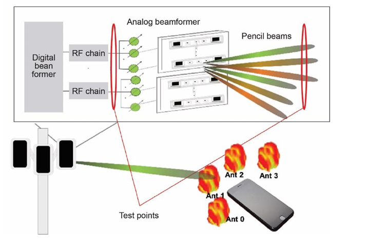 Figure 1. An example of extreme hybrid beamforming, FR3 upper mid-band base station
Ensuring that the channel model accurately captures the intra- and inter-cluster angular characteristics is essential when conducting system simulations or testing the actual performance of xMIMO base stations in RAN and Open RAN configurations. In addition, dynamic channel models are necessary for evaluating beam management and precoding adaptation over user equipment movement. These channel models consider transitions between line-of-sight / non-line-of-sight and blockage conditions.
However, the current 3GPP GSCM channel models lack the accuracy needed to develop extreme beamforming algorithms with highly directive pencil beams. To address that, a new 3GPP RP-234018 Release 19 technical study item on channel modeling enhancements for 7 to 24 GHz for New Radio (NR) was initiated.
To test the upper mid-band for FR3, test engineers need:
- Phase and time coherent multichannel emulation.
- Semi-deterministic and/or deterministic channel models.
- Accurately calibrated equipment for phase and amplitude measurements.
- Comprehensive measurement and analysis tools.
6G FR3 system testing requires phase and time-coherent multichannel emulation using semi-deterministic and deterministic channel models. From the physical layer (PHY) to the application layer, key performance metrics for 6G FR3 testing include:
- Beam weight estimation and pointing metrics.
- Beam shape and gain.
- Sidelobe levels.
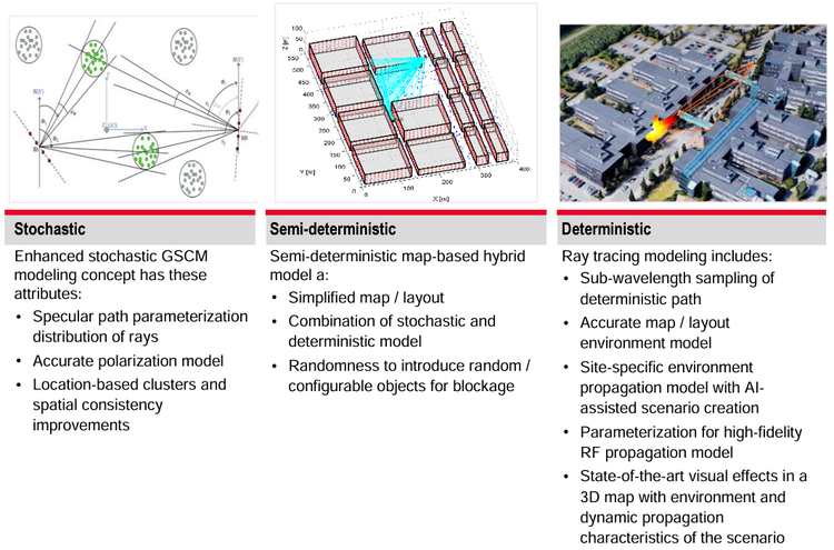 Figure 2. The three main channel modeling approaches necessary in 5G-Advanced and 6G system simulations, design, and product development and testing.
With a robust channel emulation solution, test engineers can reproduce a diverse propagation environment and emulate hardware impairments like phase noise and interference. They will need:
- Channel emulation capabilities to create realistic and highly accurate 6G FR3 environment models.
- Signal generation capabilities to provide the necessary 6G transmit waveform to the channel emulator.
- Performance metrics, including beamforming gain, beam width, and sidelobe levels.
- Software tools to perform phase and time-coherent multichannel emulation and create geometry-based stochastic channel models.
- Testing environment to reproduce propagation environments and ensure comprehensive testing.
Keysight 6G FR3 system test solution includes a channel emulator, channel emulation software, and an MXG signal generator.This solution creates realistic and highly accurate stochastic and deterministic models for mimicking 6G FR3 components and systems. The MXG signal generator provides the signal input to the FR3-capable channel emulator. The channel emulator also supports ISAC for detecting and tracking objects.
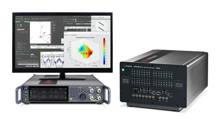 Figure 3. The Keysight 6G FR3 system test solution
The Bottom Line
Figure 3. The Keysight 6G FR3 system test solution
The Bottom Line
Precise channel emulation is crucial for 6G FR3. Accurate channel models are needed to support advanced 6G features and allow for realistic testing of 6G technologies, such as mMIMO and beamforming, under various conditions to understand how these technologies will perform in real-world scenarios. Additionally, it supports advanced use cases like ISAC, which require detailed knowledge of the channel characteristics to function effectively.
Be prepared for 6G and the challenges it brings onboard and accelerate your 6G prototyping before releasing standards using Keysight solutions for channel modeling and emulation for FR3 MIMO, mMIMO, xMIMO, and ISAC.
The post Unlocking the Potential of 6G FR3 appeared first on ELE Times.
NVIDIA Accelerated Quantum Research Center to Bring Quantum Computing Closer
Courtesy: Nvidia
As quantum computers continue to develop, they will integrate with AI supercomputers to form accelerated quantum supercomputers capable of solving some of the world’s hardest problems.
Integrating quantum processing units into AI supercomputers is key for developing new applications, helping unlock breakthroughs critical to running future quantum hardware and enabling developments in quantum error correction and device control.
The NVIDIA Accelerated Quantum Research Center, or NVAQC, announced today at the NVIDIA GTC global AI conference, is where these developments will happen. With an NVIDIA GB200 NVL72 system and the NVIDIA Quantum-2 InfiniBand networking platform, the facility will house a supercomputer with 576 NVIDIA Blackwell GPUs dedicated to quantum computing research. “The NVAQC draws on much-needed and long-sought-after tools for scaling quantum computing to next-generation devices,” said Tim Costa, senior director of computer-aided engineering, quantum and CUDA-X at NVIDIA. “The center will be a place for large-scale simulations of quantum algorithms and hardware, tight integration of quantum processors, and both training and deployment of AI models for quantum.”
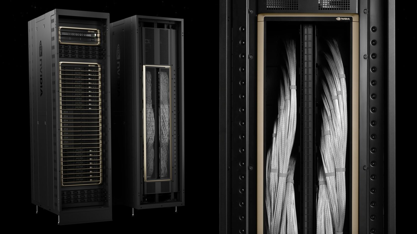 The NVAQC will host a GB200 NVL72 system.
Quantum computing innovators like Quantinuum, QuEra and Quantum Machines, along with academic partners from the Harvard Quantum Initiative and the Engineering Quantum Systems group at the MIT Center for Quantum Engineering, will work on projects with NVIDIA at the center to explore how AI supercomputing can accelerate the path toward quantum computing.
“The NVAQC is a powerful tool that will be instrumental in ushering in the next generation of research across the entire quantum ecosystem,” said William Oliver, professor of electrical engineering and computer science, and of physics, leader of the EQuS group and director of the MIT Center for Quantum Engineering. “NVIDIA is a critical partner for realizing useful quantum computing.”
There are several key quantum computing challenges where the NVAQC is already set to have a dramatic impact.
Protecting Qubits With AI Supercomputing
Qubit interactions are a double-edged sword. While qubits must interact with their surroundings to be controlled and measured, these same interactions are also a source of noise — unwanted disturbances that affect the accuracy of quantum calculations. Quantum algorithms can only work if the resulting noise is kept in check.
Quantum error correction provides a solution, encoding noiseless, logical qubits within many noisy, physical qubits. By processing the outputs from repeated measurements on these noisy qubits, it’s possible to identify, track and correct qubit errors — all without destroying the delicate quantum information needed by a computation.
The process of figuring out where errors occurred and what corrections to apply is called decoding. Decoding is an extremely difficult task that must be performed by a conventional computer within a narrow time frame to prevent noise from snowballing out of control.
A key goal of the NVAQC will be exploring how AI supercomputing can accelerate decoding. Studying how to collocate quantum hardware within the center will allow the development of low-latency, parallelized and AI-enhanced decoders, running on NVIDIA GB200 Grace Blackwell Superchips.The NVAQC will also tackle other challenges in quantum error correction. QuEra will work with NVIDIA to accelerate its search for new, improved quantum error correction codes, assessing the performance of candidate codes through demanding simulations of complex quantum circuits.
“The NVAQC will be an essential tool for discovering, testing and refining new quantum error correction codes and decoders capable of bringing the whole industry closer to useful quantum computing,” said Mikhail Lukin, Joshua and Beth Friedman University Professor at Harvard and a codirector of the Harvard Quantum Initiative.
Developing Applications for Accelerated Quantum Supercomputers
The majority of useful quantum algorithms draw equally from classical and quantum computing resources, ultimately requiring an accelerated quantum supercomputer that unifies both kinds of hardware.
For example, the output of classical supercomputers is often needed to prime quantum computations. The NVAQC provides the heterogeneous compute infrastructure needed for research on developing and improving such hybrid algorithms.
 Accelerated quantum supercomputers will connect quantum and classical processors to execute hybrid algorithms.
New AI-based compilation techniques will also be explored at the NVAQC, with the potential to accelerate the runtime of all quantum algorithms, including through work with Quantinuum. Quantinuum will build on its previous integration work with NVIDIA, offering its hardware and emulators through the NVIDIA CUDA-Q platform. Users of CUDA-Q are currently offered access to Quantinuum’s System H1 QPU hardware and emulator for 90 days.
“We’re excited to collaborate with NVIDIA at this center,” said Rajeeb Hazra, president and CEO of Quantinuum. “By combining Quantinuum’s powerful quantum systems with NVIDIA’s cutting-edge accelerated computing, we’re pushing the boundaries of hybrid quantum-classical computing and unlocking exciting new possibilities.”
QPU Integration
Integrating quantum hardware with AI supercomputing is one of the major remaining hurdles on the path to running useful quantum hardware.
The requirements of such an integration can be extremely demanding. The decoding required by quantum error correction can only function if data from millions of qubits can be sent between quantum and classical hardware at ultralow latencies.
Quantum Machines will work with NVIDIA at the NVAQC to develop and hone new controller technologies supporting rapid, high-bandwidth interfaces between quantum processors and GB200 superchips.
“We’re excited to see NVIDIA’s growing commitment to accelerating the realization of useful quantum computers, providing researchers with the most advanced infrastructure to push the boundaries of quantum-classical computing,” said Itamar Sivan, CEO of Quantum Machines.
 The NVIDIA DGX Quantum system comprises an NVIDIA GH200 superchip and Quantum Machines’ OPX1000 control system.
Key to integrating quantum and classical hardware is a platform that lets researchers and developers quickly shift context between these two disparate computing paradigms within a single application. The NVIDIA CUDA-Q platform will be the entry point for researchers to harness the NVAQC’s quantum-classical integration.
Building on tools like NVIDIA DGX Quantum — a reference architecture for integrating quantum and classical hardware — and CUDA-Q, the NVAQC is set to be an epicenter for next-generation developments in quantum computing, seeding the evolution of qubits into impactful quantum computers.
The post NVIDIA Accelerated Quantum Research Center to Bring Quantum Computing Closer appeared first on ELE Times.
A high-performance current source

The ever innovative and prolific Mr. Woodward has offered “PWM-programmed LM317 constant current source,” an intriguing programmable constant current source which elicited a lively conversation in its comments section. A Zen paradox arose: if the addition of a capacitor between ground and the LM317 ADJ pin reduces the power supply-induced ripple current delivered to the load while also reducing the impedance seen by the load (making it a less “Ideal” current source), is it a better or worse “constant current source”? To answer the question, it must also be considered that the capacitor also slows the response to load current changes which result from alteration of the PWM duty cycle. In the end, the answer depends on the application. But I’m sure a Zen master would have a better answer to the question than “it depends.”
Wow the engineering world with your unique design: Design Ideas Submission Guide
Even without the capacitor, the time constant and non-linear nature of the design idea’s (DI’s) PWM-driven circuit has limitations if used as a source of AC signals. Of course, the title of the DI makes it clear that supplying AC current to the load was not a performance goal. But one of the commenters was interested in delivering both AC and DC currents.
Basic LM317 current sourceI wondered if the subcircuit consisting of the LM317 and resistors Rs and Rc could form the basis for such a circuit if it were driven from a suitable control current. In Figure 1, the first step to investigating this was to simulate a basic LM317 current source [1] made of U1 and Rs1 to drive load RL1. The load current is 10 mA.

Figure 1 A series of LM317 circuits investigated in simulation and on the test bench for suitability as a current source.
The circuit’s broadband PSRR was simulated, measured in ohms, and defined as the ratio of the AC voltage of the V1 supply to the AC current through RL1. From DC to almost 1 kHz, the result was a little over 100 kΩ, falling to a bit below 10kΩ at 10kHz. So far, so good. Next, the candidate subcircuit containing U2 was tested. Ideal infinite impedance DC current source I1 (chosen to ensure no degradation of subcircuit performance) arranged for RL2 to also receive 10 mA DC. I expected pretty much the same PSRR here. But to my surprise, the DC to 1kHz impedance had fallen to a little under 2 kΩ and to a bit more than 100 Ω at 10 kHz!
Looking closer, there was no current at all flowing through the LM317 ADJ pin, not even the datasheet’s nominal 50 µA DC. As a result, nor was there any AC current flowing through either Rc2 or the ADJ to explain the PSRR drop. Clearly, the LM317 file [2] I was using for simulation was not suitable for testing PSRR. There are other files from the site listed in the footnote which I’ll investigate at a later date, but for now I decided instead to do some good old lab bench tests.
Bench TestsThe circuit I’ve bench-tested for PSRR is the one which has U3 as its central element. The result was much closer to but also better than the simulated U1: 500 kΩ from DC to 1 kHz, falling to 360 kΩ at 10 kHz and 80 kΩ at 50 kHz. But while I was on the bench, I started to look closely at some other things.
The U3 circuit works by subtracting a voltage drop, Vdrop, across Rc3 from the LM317’s Vref (the voltage difference between OUT and ADJ) and applying Vref – Vdrop across Rs3. Careful attention must be paid to the accuracy of Vdrop, which is challenge enough. But then there is Vref; what are its limits?
I decided to make some DC measurements. I have eight Texas Instruments LM317KCS IC’s (TO-220 package), all with same date code marking. Using the U4 circuit, I measured the Vo (OUT) of each of them with V4 set to 12 VDC. Vo ranged from 1.243 V to 1.263 V, a 20-mV difference. For one of them, I set V4 to 15 V for 5 minutes, and then to 25 V for the same time period.
After these time intervals elapsed, the measurements revealed a drop of 27 mV in Vo. This is more than the 5 mV at 25°C that comes from the spec’s line regulation of .04% per 1-V line voltage change. So, I rechecked my measurements but got the same result. From all these measurements, it’s impossible to determine the limits of Vref over different IC’s, load currents, DC input voltages, and junction temperatures of an arbitrary circuit. Then of course, there’s Noah’s revenge: every 40 days the long-term stability parameter could gift us with a 1% of Vref shift: 12.5 mV. Looking at all of this, I settled on the spec’s reference voltage limit of 1.25 V ± 50 mV for Vref. So what is the impact of this ambiguity?
ImplicationsWe do want a programmable supply, so let’s stick with the U2 configuration and defer considerations for a practical programmable current source in place of I1. Regardless of the resistor values, the current that that circuit delivers to the load is:
ILoad = Vref / Rs + (Iadj – I1) * Rc / Rs
The maximum value of ILoad, Imax, occurs when I1 is zero. When the circuit is asked to deliver Imax/10, (Iadj – I1) * Rc will ideally be set to about .9 * Vref. But now ILoad is equal to 125 ± 50mV; a ± 40% variation! Things get worse if less than Imax/10 is required. I welcome suggestions as to how to deal with the limited accuracy and operational range seen here. But for now, let’s consider the Figure 2 circuit.

Figure 2 Darlington Q1/Q2 feeds 0-Ω load, V_LOAD, with a current. R2, R5, R4 and C2 establish stability and should be checked in assembled circuits. R1 establishes the minimum Q1 DC bias.
In Figure 2, V_Supply provides power at 12 VDC. V_IN takes on DC voltages of 10, 100 and 1000 mV to produce DC currents of 10, 100 and 1000 mA through V_LOAD. Each voltage source in the schematic produces a sine wave at a frequency of 1, 10, 100, 1000 or 10000 Hz to test PSRR (Figure 3), output impedance (Figure 4), and signal transfer (Figure 5); but only one sinusoidal source is active at a time.
Sine amplitudes for V_LOAD and V_Supply when active are 1-V peak, whereas that for V_IN is 1 mV; so that when summed with the three different DC voltages that V_IN takes on, the net voltage and current will remain positive. All simulation measurements are of currents through V_LOAD. Table 1 lists the simulated verses desired DC currents flowing through that load.

Figure 3 The PSRR impedances in ohms verses frequency as seen by V_LOAD for three different DC currents. Higher impedances are associated with more nearly ideal current sources. (The dots on the curves represent simulation measurements.)

Figure 4 The Impedance in ohms seen by V_LOAD at three different DC currents. Higher impedances are associated with more nearly ideal current sources. The dots on the curves represent simulation measurements.

Figure 5 Transfer impedances in ohms verses frequency from V_IN to V_LOAD. The design goal is a value of 1.0000. The dots on the curves represent simulation measurements.
|
DESIRED CURRENT, mA |
V_FET_OUT CURRENT, mA |
|
10 |
10.011 |
|
100 |
100.009 |
|
1000 |
999.987 |
Table 1 Desired and simulated DC currents for the circuit. Op-amp input offset voltages and other aspects of the circuit will contribute errors not accounted for here.
The AD4084-2 op-amp has a worst-case input offset voltage of 300 µV. The two of them could together contribute up to ± 600 µA in error to the load. There are also the tolerances of resistors Rc1, Rc2 and RsM to consider. The limited beta of the 2N3906 could “steal” up to 10 µA from the load; replacing it with the BC857C could significantly reduce that number. And I have conveniently avoided discussing how to generate the signals produced by the voltage source V_IN, which undoubtedly will contribute their own accuracy errors. But the goal of this DI was to investigate potential power current sources capable of handling both AC and DC currents, and I believe that what was presented here is a candidate that is worth consideration for that.
Christopher Paul has worked in various engineering positions in the communications industry for over 40 years.
Related Content
- PWM-programmed LM317 constant current source
- 1 A, 20 V PWM DAC current source with tracking preregulator
- Optimizing a simple analog filter for any PWM
- A class of programmable rheostats
- LM317 smooths but doesn’t regulate
References
- https://www.ti.com/product/LM317#tech-docs See Figure 18 of the LM317 datasheet accessible from this site.
- https://groups.io/g/LTspice/filessearch?p=created%2C%2C%2C20%2C2%2C0%2C0&q=lm317, LM317A_002.zip
The post A high-performance current source appeared first on EDN.
До зеленої трансформації спільно з Асоціацією професіоналів довкілля (PAEW)
 в КПІ")
Робитимемо спільні кроки до зеленої трансформації нашої держави спільно з Асоціацією професіоналів довкілля (PAEW) — організацією, що обʼєднує понад 7 тисяч топових енвайронменталістів, науковців і практиків (інженерів, юристів, підприємців), які реалізують ефективні реформи у сфері охорони довкі
FPGA learning made easy with a virtual university program

Altera University aims to affordably and easily introduce students to the world of FPGAs and digital logic programming tools by unveiling the curriculum, tutorials, and lab exercises that bridge the gap between academia and real-world design work. The program comprises four courses focused on digital logic, digital systems, computer organization, and embedded systems.
This university program will offer professors, researchers, and students access to a broad collection of pre-developed curricula, software tools, and programmable hardware to help accelerate the FPGA learning experience. Moreover, professors can restructure the lab work with pre-developed curricula and hands-on lab kits.

The program aims to accelerate the FPGA learning experience by making available a broad collection of pre-developed curricula, software tools, and programmable hardware. Source: Altera
“We established Altera University with the singular goal of training the next generation of FPGA developers with both the AI and logic development skills needed to thrive in today’s modern workforce,” said Deepali Trehan, head of product management and marketing at Altera. “Through Altera University, we’re enabling professors to bring real-world experiences to their students using cutting-edge programmable solutions.”
Altera is also offering discounts on select FPGAs for developing custom hardware solutions. Then there is a 20% discount on select Agilex 7 FPGA-based development kits. The company also offers a 50% discount on using LabsLand, a remote laboratory with access to Altera FPGAs.
Altera University also offers higher-level FPGA courses that include an AI curriculum to ensure that students can stay aligned with the latest industry trends and develop an understanding of usage models for FPGAs in the AI workflow.
Altera University’s academic program website provides more information on curricula, software tools, and programmable hardware.
Related Content
- All About FPGAs
- FPGAs for beginners
- Power-aware FPGA design
- FPGA programming step by step
- Embedded design with FPGAs: Development process
The post FPGA learning made easy with a virtual university program appeared first on EDN.
ST’s Automotive MCU technology for next-generation vehicles
Author: STMicroelectronics
ST has been serving customers in the automotive market for over 30 years and provides them with a range of products and solutions covering most applications in a typical vehicle. As the market has evolved, so has ST’s offering, a key part of which is automotive microcontrollers (MCUs).
ST pioneered embedded non-volatile memory (eNVM) with ST10 and then introduced automotive microcontrollers with its SPC5 range based on PowerPC architecture, shipping more than one billion MCUs in automotive. Cost-effective automotive controllers from the STM8 family complemented this offer.
ST’s Stellar FamilyST’s latest generation of automotive microcontrollers is the Stellar family, which is the industry’s first Arm®-based portfolio that spans the entire automotive MCU spectrum, from low-end to high-end solutions. These advanced microcontrollers reduce complexity, ensure safety and security, and deliver optimal performance and efficiency of next-gen vehicle architectures and features. Customers can benefit from shorter development times and focus on bringing innovation and differentiation for their software-defined vehicles (SDVs) in this highly competitive market. For these reasons Stellar products are gaining momentum, particularly among our customers in Asia and Europe.
Stellar is the industry’s first family of emerging technologies after eFlash, representing the most mature and smallest memory cell automotive grade solution on the market. The Stellar family is optimized for electrification, including X-in-1 vehicle motion control computing, new vehicle architectures, zonal and domains, and safety MCUs for safety-critical subsystems, such as ADAS.
It fully supports automotive transformation by integrating multiple functions safely into a single device and allowing the continuous integration of new features in vehicles. This is made possible with key technologies, including a right choice of core technology, virtualization, Ethernet support and ground-breaking memory technology embedded in the automotive MCUs–a game changer for customers faces challenges with application memory sizing.
Stellar MCUs are based on Arm® Cortex®-R52+ technology. This high-performance processor delivers real-time virtualization support for time-critical secure and safety systems. It can run multiple applications simultaneously with freedom from interference. And thanks to fully programmable auxiliary cores it is possible to accelerate specific functions, such as routing, low power management, digital filtering while offloading the main cores.
“As the driver experience continues to evolve in the age of AI and software-defined vehicles, advancing automotive functional safety, flexibility and real-time performance capabilities is essential,” said Dipti Vachani, senior vice president and general manager, Automotive Line of Business, Arm. “Built on Arm, the Stellar microcontroller family taps into the Arm compute platform’s advanced safety and real-time features, as well as the broad Arm software ecosystem. This enables car manufacturers to comply with strict safety regulations while implementing innovative features that keep them at the forefront of the automotive industry.”
Stellar MCUs enable the introduction of ethernet capabilities in vehicles and is the first ST MCU embedding an Ethernet switch. Thanks to Ethernet, data exchange is more efficient, and flexible, supporting the needed gigabit throughput, with a higher level of security. By supporting various in-vehicle communication topologies, such as Ethernet ring, automotive MCUs fulfill the promise of halving the length of the cross-car wiring cables and manufacturing costs.
Phase Change Memory is set to redefine what is possible in vehicle softwareStellar MCUs, with the embedded Phase Change Memory (PCM) technology and its flexibility, transform the process of Over-the-Air (OTA) updates. In the automotive industry, OTA updates are crucial for adding new features and safety or security patches without physical intervention. However, this flexibility often requires careful consideration of future memory needs, which can lead to increased costs and complex planning.
ST’s PCM innovation is no ordinary memory. Not only is it the industry’s smallest memory cell for automotive MCU, but it is pioneering a transformative breakthrough in automotive and set to redefine what is possible in vehicle software. Thanks to ST’s innovative PCM technology, memory capabilities are reaching a new level of sophistication. This is not just about memory performance. It is a forward-thinking solution that brings adaptability and lasting value to the automotive landscape enabling the final developers to continuously improve and upgrade functions.
As vehicles become increasingly software-defined, the ability to introduce new features and enhancements is essential. PCM’s groundbreaking technology will support the shift toward more adaptable, future-focused vehicles, giving automakers new ways to refine experiences as vehicles continue to advance.
Additionally, PCM delivers the ability to support uninterrupted OTA updates. PCM securely stores updates without impacting the vehicle’s current operations. Thanks to concurrent read and write capabilities, the new software download does not interfere with the application code already running on the MCU, ensuring continuous performance during the update process.
Stellar P, designed for the integration of multiple functions, and Stellar G, for the realization of Software-Defined Vehicles (SDV) zonal controllers, are two series leveraging ST’s internally developed eNVM. They are built on 28nm FD-SOI technology, allowing them to achieve maximum frequency with lower power consumption and enhanced radiation immunity. Stellar is the first 28nm product certified for functional safety and will enter production by the end of this year.
The Stellar family also enables the X-in-1 growing trend toward more affordable electromobility, with the decisive switch from fossil to electrically powered vehicles. X-in-1 powertrain solutions combine multiple components into a single ECU, allowing manufacturers to create efficient, compact, and cost-effective performing vehicles.
Stellar offers scalable X-in-1 implementation, accommodating a growing number of ECUs from low to high integration levels. This solution supports increasingly complex X-in-1 systems by providing enhanced availability of cores, analog components, and I/O capabilities.

“As a global leader in lithium-ion batteries, Sunwoda provides stable and reliable electronic system solutions for automotive suppliers worldwide. Our new collaboration with STMicroelectronics focuses on developing solutions using ST’s advanced Stellar microcontrollers and proprietary production processes, which primarily include battery management systems, and VDC/Zonal and body control functions. Together, we aim to provide intelligent solutions that enhance the next generation of energy vehicles in China and globally,” said Wang Mingwang, founder, Sunwoda.
2. FD-SOI technology to achieve the max possible frequency at the lower power consumption and to strengthen radiation immunity
3. New powerful over-the-air methodology and true EEPROM capabilities
4. A set of ethernet-related IPs (MAC, MACSec, switches) that enable distribution of high volume data, allow different topologies of in-vehicle communication, and reduce the vehicle manufacturing cost
5. Fully programmable auxiliary cores that accelerate specific functions such as routing, low power management, digital filtering while offloading the main cores
As part of the expanded roadmap for automotive MCUs, ST will introduce its market-leading general-purpose STM32 microcontroller platform to the automotive sector. The STM32 platform is well recognized for its cost optimization, simplicity, and reliability. Augmented with automotive grade quality and safety, STM32A will achieve up to ASIL B standards. This platform will be designed to handle edge actuation, from the simplest functions to more sophisticated single tasks, all at optimized costs. It will be particularly well-suited for applications like motor control in vehicle systems, including windows, mirrors, and roofs.
Best of industrial and automotive worlds: towards converged futureOver time, the convergence of the industrial and automotive hardware and software platforms will combine the best of both worlds. Automotive brings strong security expertise and industrial is built on strong Internet of Things and artificial intelligence solutions. The converged future will share hardware technologies, cores, and a common ecosystem of tools and software support. Such convergence will enable customers to seamlessly transition between solutions, offering simplification and full scalability to innovate faster.
Edge AI technology is one example where we see what is being adopted now in industrial applications benefiting automotive in the future. Neural accelerator technology and the associated tools that enable developers to easily implement AI in their applications, whatever their level of data science expertise, will enhance automotive systems in the future. ST has spent approximately 10 years investing in the development of microcontrollers, smart sensors, and AI software tools to meet the needs of our customers and harness the power of edge AI.
While AI adoption in automotive—beyond autonomous driving—is still in its initial stages, there are emerging trends of promising use cases for system optimization, energy efficiency, and problem-solving. For example, virtual sensors can measure rotor temperatures, and predictive maintenance can ensure vehicle reliability. As the number of sensors in vehicles heavily increases, AI will play a key role in virtualizing many of them, further enhancing automotive performance. Security is another area where we see the convergence of industrial and automotive bringing significant benefits.
This future will be based on the most advanced and more efficient 18nm process technologies. ST’s advanced technology portfolio for automotive MCUs spans from 40 to 28 to 18nm, selected to optimize product performance and cost.
The benefits of the IDM model for our customersAs an integrated device manufacturer (IDM), ST develops fundamental semiconductor process technologies, creates core intellectual property (IP), designs products using these technologies and IP, and manufactures, tests and packages them using owned facilities or through partnerships. This brings several benefits for our customers:
- Processes designed and refined to meet the applications needs of our customers in various markets.
- IP blocks optimized for specific functions and systems, owned by ST.
- Manufacturing processes are optimized for key performance and yield through the tight teamwork between process, product, and operational teams.
- Control of manufacturing capacity and creation of flexible, reliable supply chains.
This is particularly important for our automotive customers.
An example of these benefits is the combination of FD-SOI and PCM technologies that ST has developed for its Stellar microcontrollers. ST was one of the key innovators in both technologies, working with partners to bring them to market. ST’s ability to master the technology and tailor it to automotive applications has resulted in products with unique benefits. ST’s implementation of PCM technology has allowed the creation of the smallest physical memory cell in the industry delivering 2x the memory density of alternatives.
Thanks to the high-energy efficiency, high reliability, and radiation immunity of this memory technology, ICs designed in FD-SOI with embedded PCM meet the most stringent requirements of automotive applications. ST’s PCM technology achieves automotive requirements for AEC-Q100 Grade 0 with an operating temperature up to +165°C. The patented technology supports high-temperature data retention, including during solder reflow, so firmware can be uploaded before soldering.
Ecosystem plays a key role for transformationAn extensive partner ecosystem from developer tools to specific libraries for safety, security, and data exchange and distribution, augmenting ST’s portfolio capabilities further complements this leading technology. This will also provide the necessary simplification, aiding our customers in their transformation journey towards software-defined vehicles.

“STMicroelectronics and Green Hills Software are working closely together to deliver innovative integrated hardware and software solutions that address the growing challenges automotive OEMs and Tier 1s face in next generation vehicle zonal architectures.” said Dan O’Dowd, Founder and CEO at Green Hills Software. “Green Hills production-proven safety-certified RTOS and tools, coupled with ST’s Stellar SR6’s unique communication IP, deliver advanced fault tolerant zonal networking that enables significant per-vehicle cost savings while reducing time-to-market.”
“With MICROSAR Classic, we enable our customers with safe and secure basic software for ECUs for a wide range of use cases. Thanks to many years of close cooperation with ST, the corresponding support for the new Stellar MCUs is already available,” says Jochen Rein, Director of the Product Line Embedded Software and Systems at Vector. “By integrating Stellar’s advanced hardware with Vector’s robust software, customers get the highest level of safety and reliability for both ADAS applications and to successfully manage the transition to Software-Defined Vehicles.”
“iSOFT is a leading developer of automotive operating systems in China and the premium partner of AUTOSAR for China’s infrastructure software. Since the introduction of its collaboration with ST in 2016, iSOFT has become ST MCAL agent in China. This includes multiple microcontrollers such as SPC58/SPC56/STM8A, and the companies will also engage in a deeper strategic cooperation on the newly introduced Stellar family that will support EasyXMen Open Source Operating System in the future.” Luo Tong, Vice President, iSOFT

“Neusoft Reach’s software platform, NeuSAR, leads the mass production of China’s full-stack “AUTOSAR +Middleware,” widely used in next-gen ADAS, chassis, power, and body control systems. Neusoft Reach provides complete solutions based on ST’s SPC5 and Stellar E series automotive MCU, including application/basic software, bootloader, refresh, and simulation, which will be complemented with the new gen of Stellar P and G series. Both companies will work together to create a higher level of automotive-grade software and hardware integrated solutions to help OEMs and tier 1s to bring efficient, personalized, and differentiated functions and accelerate SDV innovation.” Jipeng Wang, Director, NeuSAR CP Products BU, Neusoft Reach
ConclusionBy building on common foundations across product dimensions and focusing on robust automotive quality, ST serves a wide market with a comprehensive product range that is both “broad”—spanning from as low as 128 KB to 64 MB memory, single to multicore computation with virtualization—and “deep,” with each series tailored for specific functions: Stellar P and G series focus on integration, and STM32A will be optimized for value, targeting single-core applications that prioritize efficiency and simplicity.
ST’s expanded automotive microcontrollers roadmap focuses on helping its customers to reduce complexity, improve efficiency, while ensuring the highest security and safety standards for next-gen cars. It addresses electrification, personalization, automation, and connectivity.
The post ST’s Automotive MCU technology for next-generation vehicles appeared first on ELE Times.
Pages


![[link]](https://i.redd.it/bljdn7pqs0ue1.jpeg)