


Збирач потоків
КПІшники долучилися до освітньо-інноваційного проєкту PolyTECH Project 2026

☑️ Студенти та представники КПІ взяли участь у дводенному хакатоні PolyTECH Bootcamp Kyiv, організованому інноваційним парком UNIT.City за сприяння Міністерства освіти і науки України. Учасники працювали над власними проєктами разом із менторами, презентували результати експертному журі та спілкувалися з представниками бізнесу.
Єдність у дії: доступні культурні простори як основа розвитку громад

👥 КПІ ім. Ігоря Сікорського став платформою для діалогу про доступні культурні простори — «Єдність у дії: доступні культурні простори як основа розвитку громад»
Перше знайомство нового складу «Формула Студент КПІ» відбулося!

⚙️ Близько 100 амбітних студентів приєдналися до команди, щоб прокачувати навички в інженерії, бізнесі та комунікаціях і разом пройти шлях від перших креслень до боліда, який вийде на трек.
5G to 6G: AI moves into the network

Traditionally, every generation of cellular technology has been mostly about moving data faster. However, 6G is shaping up to be a different kind of upgrade. The industry’s focus is shifting from how fast a network can move data to what new services and experiences it can deliver, with artificial intelligence enabling this shift.
6G is being designed to embed AI deeper into the radio access network (RAN) and core, enabling the network to predict demand peaks before congestion sets in and manage radio resources in real time. That same intelligence could also help the network make use of its own infrastructure and wireless signals to provide data and gather information about the physical environment.
AI already exists in 5G networks, but 6G is designed to integrate these capabilities more deeply into the network architecture. 6G is still being defined through the 3rd Generation Partnership Project (3GPP) standards process, and many of these technologies are in the trial stage. Still, the direction is becoming clear as AI, distributed computing, and sensing are becoming as integral as new frequencies, lower latency, and data rates.
6G standardization & 3GPP3GPP started to study 6G in Release 19, which was completed in December 2025. Release 20 evaluates foundational items for 6G, including studies of AI, sensing, and new architecture of the 6G network, and it is expected to be completed by 2027. Release 21 is now open for contributions and will be the first normative 6G specifications, pending finalization of its scope and timeline, and is expected to build on top of Release 20 studies and be completed by 2030.
Commercial 6G systems are still expected around 2030, although pre-commercial deployments and field trials will appear earlier. Many of the technologies being considered for 6G are already being introduced through 5G-Advanced, giving vendors and operators a chance to test capabilities such as AI-driven network optimization and integrated sensing and communication (ISAC) before committing to larger 6G deployments.
At the same time, 6G development is not limited to consumer networks. Governments and defense departments are also exploring potential use cases, particularly where communications, computing, sensing, and real-time decision-making need to work together. The U.S. Department of Defense is exploring 6G technologies and prototypes for military applications, adding another potential source of demand for early 6G systems.
The U.S. government’s Mission 6G 28 initiative is another example of this push toward early testing. The initiative is encouraging industry-led demonstrations of technologies, including AI-driven networking and integrated sensing, ahead of the 2028 Los Angeles Olympic Games. These demonstrations use pre-standard technology, providing an early look at which concepts can move from research into real-world environments.
Vendors are also developing tools to support these early trials, giving operators and research and development teams a way to test new capabilities before the standards are finalized.
 3GPP’s timeline for Release 21 (Source: 3rd Generation Partnership Project)
The standards process provides the industry with key milestones to watch. Release 20 is expected to conclude in 2027, followed by the development of the normative 6G specification in Release 21 and the final protocol freeze in March 2029. After that, the focus shifts to operators and equipment manufacturers to turn those specifications into reliable systems.
AI-RANOne of the clearest examples of AI moving into the network is in the RAN, which includes the base stations and antennas that connect devices to the cellular network. Traditionally, RAN equipment has been built around proprietary hardware and custom silicon designed for telco-specific functions with long upgrade cycles. AI is starting to challenge that model, but the industry is not taking one single approach.
Ericsson is taking a more evolutionary approach. The company is embedding AI capabilities into the RAN infrastructure that operators already have, with the goal of improving performance without a costly, large-scale hardware replacement. Early trial results point to real gains in efficiency and throughput, particularly around scheduling and radio resource management.
Nokia and Nvidia are pushing something more transformative. Their AI-RAN uses graphics processing unit (GPU)-based computing alongside traditional telco workloads, turning the RAN into a more flexible compute platform.
Nvidia backed this vision with a $1 billion investment in Nokia, and the two companies already have live trials running with T-Mobile. Putting more GPUs into the RAN brings additional computing capacity but also higher power consumption, cooling requirements, and infrastructure costs. Operators will ultimately have to decide whether the revenue from running AI workloads at the edge is enough to justify those costs.
If operators mostly want better network performance, adding AI to existing RAN infrastructure may be enough. However, the case for GPU-based AI-RAN becomes stronger if operators see an opportunity to turn that additional compute into a new business around distributed AI workloads.
The 6G coreAI is also starting to reshape the network core, the part of the network responsible for routing traffic, managing connections, and allocating resources. In May 2026, 3GPP advanced two competing approaches for integrating AI into the 6G core, with both now being studied in parallel.
The first, Solution Variant #18.1, puts AI directly into the core through new, agent-based network functions. These functions could interpret an intent from a user or application and orchestrate existing network functions to carry it out.
The second, Solution Variant #18.3, keeps AI separate from the core. A dedicated AI domain would interact with existing network functions through a translator function, allowing AI to optimize and orchestrate the network without fundamentally changing the core itself.
 Two approaches for integrating AI into the 6G core (Source: ABI Research)
Variant #18.1 is being pushed primarily by Chinese vendors and operators, including Huawei, ZTE, and the major Chinese carriers, while Variant #18.3 has support from Western vendors and operators including Nokia, Ericsson, AT&T, T-Mobile, Qualcomm, and Google. SK Telecom is notably involved in both, reflecting the fact that the industry has not settled on a single path.
For now, 3GPP is keeping both options open. Where AI ends up sitting in the core will shape network architecture and vendor influence for years.
Integrated sensing and communicationAs AI makes the network more capable of making decisions and managing itself, sensing can give it more information about the physical environment around it. ISAC uses its existing wireless signals for both communication and sensing, allowing cellular infrastructure to detect and track objects without dedicated sensing equipment.
Recent trials are starting to show what it could look like in practice. For example, in July 2026, AT&T and Ericsson used existing 5G infrastructure outside the AT&T Stadium in Texas to detect, locate, and track multiple drones flying between 300 and 400 feet. The system used existing massive multiple-input/multiple-output radios, signal processing, and AI-enabled sensing rather than a separate radar system.
The demonstration is a useful proof point, but it is not yet a replacement for dedicated radar. It’s more likely a near-term role as an additional layer of sensing, particularly in places where cellular infrastructure is already widely deployed. Drone detection, perimeter security, industrial sites, ports, and logistics facilities are the likely first use cases.
The bigger test will be whether ISAC can move beyond controlled trials and demonstrate performance across different environments, weather conditions, distances, and object types. If ISAC can handle those conditions, it could give AI-driven networks another important input, allowing them to make decisions based on what is happening in the physical environment and inside the network.
What to watchThe next few years will show whether 6G can deliver on the larger idea that it is less about a faster connection and more about the network becoming an intelligence platform. The clearest checkpoints are on the standards calendar: Release 20 studies conclude in 2027, the architecture is due to be finalized in 2028, and the first normative 6G specs freeze in March 2029. This will determine the technical standards, but what operators do in practice comes down to whether AI, distributed computing, and sensing can create enough value to justify the cost and complexity of putting them deeper into the network.
This is what truly differentiates 6G from previous generations. The network is becoming part of the computing infrastructure and can process AI workloads closer to the source, make decisions about how network resources are used, and gather information about the physical environment. That moves 6G beyond the traditional role of connecting devices and toward a more intelligent network.
This is a follow-up to ABI Research’s 5G & 6G: Adoption, Technologies and Use Cases.
The post 5G to 6G: AI moves into the network appeared first on EDN.
Zork on a Steam Controller: when the gamepad becomes a mainframe
A Steam Controller, Valve’s gamepad, now runs Zork, the famous text adventure from 1980. Owen Feldman has written an Intel 8080 emulator in Rust that runs directly on the controller’s microcontroller. The emulator boots CP/M, the operating system of that era, and the Z-machine, the virtual machine that interprets Infocom games. The result is a fully playable game, with the computer connected via USB acting as a terminal.
The Arm Cortex-M4 and the 8080 emulatorThe heart of the project is the Steam Controller’s main microcontroller, an Arm Cortex-M4. According to Feldman, this chip is orders of magnitude more powerful than the entire Apple IIc, the computer on which many people played Zork in the 1980s. The Intel 8080 emulator was written from scratch in Rust, a language known for safety and performance. The emulator, together with the Z-machine and Zork, is installed on the controller using the firmware update tool included in the Steam package for Linux.
The game needs no graphical resources: Zork is text only. However, the controller has neither a screen nor a keyboard. Feldman therefore wrote a small server application that runs on the connected computer. This application displays the game text and sends commands to the engine over USB. In practice, the PC becomes a serial terminal, while the gamepad does all the computational work.
The failure and repair with a Raspberry Pi PicoDuring the process, Feldman damaged his Steam Controller. The original firmware was compromised and the gamepad no longer responded. To repair it, he used a Raspberry Pi Pico soldered to the debug pins on the board. With the Pico he restored the original firmware, bringing the controller back to life. This step shows how useful it is to have a spare microcontroller for low-level debugging.
The project is documented in Owen Feldman’s video, where he shows the development process and the repair. It is a perfect example of how modern consumer hardware can be pushed beyond its limits. A gaming pad, designed for input and vibration, becomes a complete computer capable of running an operating system and a retro gaming classic.
- The gamepad’s Arm Cortex-M4 microcontroller runs the Intel 8080 emulator.
- CP/M and the Z-machine run inside the emulator, with no external hardware.
- The PC connected via USB acts as a terminal for text and commands.
- A Raspberry Pi Pico made it possible to restore the firmware after a failure.
For those who want to replicate the project, you need a Steam Controller, a computer with Steam for Linux, and a bit of patience. The most delicate part is flashing the firmware: a mistake can render the gamepad unusable, as happened to Feldman. Having a Raspberry Pi Pico available for debugging is a smart precaution. In addition, those who want to experiment with microcontrollers may find the Pico Primer kit with sensors and tutorials useful, although for this project only the bare Pico is needed.
Source: https://youtu.be/M5XUR8Fnjf4?si=IhDVd-LKypGjz5rw
The post Zork on a Steam Controller: when the gamepad becomes a mainframe appeared first on Open Electronics.
Neon lamps and Krypton 85

You don’t have to be Superman (or even just use phone booths as changing stations) to find this author’s recent research results disturbing.
I was recently looking for some information about neon lamps when I came across a series of websites with content which, courtesy of my blissful naïveté, I found rather jarring. I merged a collection of screen shots into one image for your ease of perusal (Figure 1).

Figure 1 Warning: this collection of screen shots may be angst-inducing.
Looking further into the “radioactive additive” matter, I found a paper about that Krypton stuff (PDF). And looking further yet, I came across two more screen shots, which IMHO are very much deserving of your attention (Figures 2 and 3).

Figure 2 This screenshot’s information covers Krypton 85 itself.

Figure 3 And this screenshot discusses Kr-85’s uses and cancer risks.
Having been jolted into newfound awareness of the presence of radioactive material where I would never have expected it (due, again, to my own naïveté, of course.), I am reminded of how exposure to lead has been recently recognized as having no minimum exposure level that can be considered safe for anyone. Leaded gasoline, for example, is now out of use.
Mercury exposure is another example. And X-ray exposure effects are of similar concern, albeit minimally accepted only as necessary for medical diagnostics purposes.
My sense is that the same “no minimum acceptable exposure” rule should also apply to radiation exposure from electronics components, with regard to the possibilities of “cancer induction”. And right now, for lack of such, one should handle Krypton 85-bearing items with some care and, if accidentally broken, with extreme care. Although what precise steps would be called for, I do not know.
John Dunn is an electronics consultant and a graduate of The Polytechnic Institute of Brooklyn (BSEE) and of New York University (MSEE).
Related Content
- Radon sensor embeds sizeable alpha particle detector
- Radon: Level detection, risk determination, and as-needed mitigation
- My Geiger counter doesn’t count (sob sob)
The post Neon lamps and Krypton 85 appeared first on EDN.
📰 Газета "Київський політехнік" № 31-32 за 2026 (.pdf)

Вийшов 31-32 номер газети "Київський політехнік" за 2026 рік
EEVblog 1776 - $175/Hr to Teach AI How to Automate Altium PCB Design
Renesas Introduces Smallest GreenPAK Configurable Mixed-Signal IC with Multi-Time Programmability
Renesas Electronics Corporation on 24th September, 2026, announced the SLG46801, the industry’s smallest GreenPAK configurable mixed-signal device, available in both WLCSP and STQFN packages. The 9-ball WLCSP measures just 1.155 mm × 1.155 mm and combines an ultra-small footprint with multi-time programmability, helping designers reduce PCB space in compact products such as smart rings, smartwatches, fitness bands, VR glasses and portable electronics.
Consumers are demanding smaller, more feature-rich products, while designers need to add functionality while reducing component count, PCB area and bill-of-materials (BoM) costs. The SLG46801 addresses these requirements by combining commonly used analog, timing and logic functions in a compact, low-power device. It can complement an MCU or replace multiple discrete components, helping designers reduce board space and simplify designs.
“Designers are being asked to integrate more functionality into increasingly compact products without increasing system cost or development effort, while also reducing power consumption.” said Jason Kim, Vice President and General Manager of the Core Analog Division at Renesas. “The SLG46801 expands our GreenPAK portfolio with an ultra-compact WLCSP option and flexible in-system configurability, helping customers create smaller, more feature-rich products and implement updates even after deployment.”
The SLG46801 integrates two high-speed analog comparators, configurable lookup tables, counters and delays, 10 kHz and 25 MHz oscillators, voltage-tolerant GPIOs and an I²C-compatible serial interface. These resources support sensing, control, glue logic, timing and system housekeeping functions in applications across consumer electronics, handheld devices, smart-home systems, networking and communications, computing and storage, industrial control and IoT sensor nodes.
In addition to the 9-ball WLCSP, the SLG46801 is available in a 12-lead, 1.6 mm × 1.6 mm × 0.55 mm STQFN package. The two package options allow customers to balance minimum board area with additional GPIO availability and industrial package preferences. The device also offers one of the lowest cost per GPIO in the GreenPAK family.
Renesas is a leader in configurable mixed-signal technology, with more than four billion GreenPAK devices shipped worldwide. GreenPAK ICs enable designers to combine analog and digital system functions in small, low-power devices that can be configured using the Renesas Go Configure Software Hub. The free GUI-based development environment helps customers develop custom hardware functions without the need for additional discrete components or complex firmware development.
The SLG46801 includes multi-time programmable non-volatile memory that can be configured in system through its I²C interface. This allows customers to implement bug fixes, configuration changes and product upgrades after the device has been integrated into the end application, helping reduce redesign cycles and additional hardware revisions.
The device supports operation and programming across the full 1.71 V to 5.5 V supply range—the widest operating and configurable range among MTP GreenPAK devices. GPIO pins can also be repurposed dynamically for the I²C interface, maximizing flexibility in designs with limited pin availability. Optional CRC-8 and read-back protection support more robust and controlled configurable implementations.
The post Renesas Introduces Smallest GreenPAK Configurable Mixed-Signal IC with Multi-Time Programmability appeared first on ELE Times.
Cadence Expands ChipStack AI Super Agent with AI-Powered RTL Generation and PPA Optimization
Cadence on September 24, 2026, announced a new agent for the Cadence ChipStack AI Super Agent that automates front-end digital design and verification, covering power, performance and area (PPA)-driven spec-to-RTL generation, RTL analysis and refinement through natural language prompts. Building on the industry’s first agentic workflow for front-end design and verification announced in February 2026, the RTL Generation Agent extends the ChipStack AI Super Agent from autonomous verification and debug to high-quality RTL creation and optimization. In early evaluations, the RTL Generation Agent delivered an average 24% reduction in area and 18% reduction in power compared with pure foundation model code generation, while ensuring 100% functionally accurate RTL, according to Cadence.
Building on the industry’s first agentic workflow for front end design and verification announced in February 2026, this RTL Generation Agent extends the ChipStack AI Super Agent from autonomous verification and debug into high quality RTL creation and optimization.
“These latest agentic AI advancements take us from AI assisted tools to coordinated agentic workflows that behave more like virtual design engineers with expert-level command of the underlying technologies,” said Chin-Chi Teng, senior vice president and general manager in the Digital & Signoff Group at Cadence. “By pairing agentic automation of spec-to-RTL and RTL refinement with our proven implementation and signoff engines, we enable customers to achieve better design outcomes with higher productivity and stronger correlation across the design flow, further extending Cadence’s leadership in AI driven, end to end chip design.”
Cadence’s transformational approach to applying agentic AI to engineering design is founded on a hierarchy of solutions—super agents orchestrate task-specific agents, which in turn use trusted electronic design automation (EDA) software, optimized for agentic workflows. The new RTL Generation Agent converts high level specification into production ready RTL optimized for PPA.
Customer Validation from HondaEarly collaborations with Honda R&D demonstrate how these agentic AI capabilities translate into real world PPA and productivity gains on next generation SoCs.
Honda is evaluating the RTL Generation Agent on advanced automotive SoCs, where safety critical requirements and tight power and cost envelopes demand highly optimized RTL.
“As a key enabler of Software-Defined Vehicles (SDVs), AI technology for autonomous driving is advancing rapidly. However, the long development cycle of SoCs remains a major challenge. With the Cadence ChipStack AI Super Agent’s RTL Generation Agent and AI-powered automation, Honda R&D is working to improve productivity from specification through RTL development,” said Tomoya Nishino, chief engineer and general manager, Digital Engine Development Division, SDV R&D Center, Honda R&D Co., Ltd.
Smarter RTL Updates and Early PPA InsightIn addition to new RTL creation within the RTL Generation Agent, Cadence is introducing technology for design updates to existing RTL based on new requirements. This RTL upgrade flow brings AI automation to accelerate RTL revision, enabling customers to rapidly adapt legacy RTL to new architecture requirements, new PPA targets and new functional requirements. Engineers describe changes at a high level, and the agents carry out the updates while analyzing and verifying PPA and functionality.
Advancing Cadence’s Agentic AI VisionThese enhancements build on Cadence’s “Design for AI and AI for Design” strategy highlighted at CadenceLIVE and Computex, further extending the company’s leadership in AI driven chip design. From the initial ChipStack AI Super Agent launch through June’s announcement of the industry’s first fully autonomous virtual engineer for chip design, and now today’s RTL Generation Agent, Cadence continues to expand the scope of agentic workflows across the design stack. Together with the broader ChipStack, InnoStack and ViraStack AI Super Agent portfolio, they advance a scalable platform that applies AI across digital, analog and verification domains.
The post Cadence Expands ChipStack AI Super Agent with AI-Powered RTL Generation and PPA Optimization appeared first on ELE Times.
MAX7219 LED Matrix with Arduino: Wiring and Library Guide
Let’s find out how to use the MAX7219 to drive an LED matrix. Wiring, Arduino libraries and sketches will guide us through building custom graphic and numeric displays.
An LED matrix display is one of the most fascinating components for anyone starting to experiment with Arduino: with a small square module we can bring to life numbers, letters, symbols and animations that immediately catch the eye. The problem? An 8×8 matrix means no fewer than 64 LEDs to control individually: an almost impossible task without dedicated support. That is where the MAX7219 chip comes in, an IC designed specifically to simplify the management of matrix and 7-segment displays, reducing the connection to the Arduino board to just a few pins. In this article we will see how to connect the MAX7219 to an 8×8 matrix, how to use the ready-made modules available on the market and how to program everything with the LedControl library.
The MAX7219 Fig. 1 Pinout of the chip and of the display.
The MAX7219 chip has 24 pins. The 8×8 display (Fig. 1) is connected so that the rows are linked to the DIG pins and the columns to the SEG pins of the MAX7219.
Brightness is varied in software after setting the maximum current with an external resistor connected to the Iset pin. Three pins are dedicated to communication with the control board: DIN (to transfer data from the board to the chip), CS (for device selection) and CLK (for the data clock). A further pin, DOUT, is used to connect the DIN of the next chip, in case you want to chain several LED matrices together (for example to build scrolling text).
The complete schematic of the connection between the chip and the display is shown in Fig. 2, with particular emphasis on the links to the Arduino board and to a second chip. Using the MAX7219 is made even simpler by the availability on the market of modules (such as those in Fig. 3) that integrate both the chip and the LED matrix, along with the relevant wiring.
 Fig. 2 Schematic of the connection between the chip and the display.
 Fig. 3 Schematic of the connection between modules and the Arduino board.
Using a module reduces the wiring to just the connections between the module and the Arduino board, and between modules possibly arranged in a chain. Each module has 5 input pins (VCC, GND, DIN, CS/LOAD and CLK, to be connected to a board such as the Arduino UNO R3) and 5 output pins (VCC, GND, DOUT, CS and CLK, for any subsequent modules in the chain). The Arduino UNO R3 board can be replaced by the more recent Arduino UNO R4 versions, available in the Minima and WIFI models, both fully compatible electrically and in software with the previous R3. Both versions keep the same pin layout and are compatible with most shields and libraries already developed for the R3.
Programming with ArduinoSeveral libraries make programming the MAX7219 easier; among them, in particular, the LedControl library, which is very widespread and simple to use.
The basic commands are as follows:
#include “LedControl.h” LedControl LC=LedControl (DIN, CLK, CS, number_of_modules)
An object of the LedControl class is created, to which an identifying name is assigned (for example, LC). The DIN, CLK and CS parameters will be replaced with the numbers of the Arduino pins (for example: 2, 4, 3) to which the respective signals are connected.
LC.SHUT (module_number, 0/1)
Enables or disables the chip. The value 0 makes it operational, while 1 puts it in standby. On power-up, the chip is in standby mode by default. The module_number parameter identifies the module in a serial chain, numbered starting from 0.
lc.setIntensity (module_number, intensity)
Adjusts the brightness of the LEDs, with a value between 0 (minimum) and 15 (maximum). The value 0 does not turn the LEDs completely off; to do that, you need to use LC.Shutdown(module_number, 1).
lc.clearDisplay (module_number)
Turns off all the LEDs of the specified module, clearing the displayed content.
lc.setLed (module_number, row_number, column_number, state)
Turns a single LED on or off. row_number and column_number indicate the position of the LED (numbered from 0 to 7). state = true (or 1) turns the LED on, false (or 0) turns it off. Rows are numbered from 0 (top) to 7 (bottom), columns from 0 (left) to 7 (right). For example, the top-left LED occupies position (0, 0), the bottom-right one (7, 7).
lc.setRow (module_number, row_number, byte)
Lets you turn all the LEDs of a row on or off, specifying their state with a binary byte. For example, to turn on the first four LEDs of a row you use: B11110000.
lc.setColumn (module_number, column_number, byte)
Works in a similar way to setRow, but acts on a column. The byte defines which LEDs to turn on or off in the specified column. Let’s now look at some practical examples of use.
Example 1The first sketch, shown in Listing 1, is meant to display the 8 rows in sequence, one at a time, starting from the top; then the 8 columns, one at a time, starting from the left; then the 8 rows starting from the bottom; then the 8 columns starting from the right. Finally, all the LEDs are turned on gradually in pairs of rows, starting from the two middle rows and following the order: 4-5, 3-6, 2-7, 1-8. In this last phase, the lighting happens at low intensity, with brightness varying progressively from 10 to 2.
 The first sketch lights up rows and columns of the matrix in sequence.
The purpose of this sketch (Listing 2) is to gradually light up the LEDs of the matrix rows starting from the bottom, as a consequence of a voltage varying between 0 V and 5 V set by a potentiometer connected to pin A5; the comments inside the sketch describe how the gradual lighting works.
 The second sketch lights the rows gradually as the potentiometer voltage changes.
The goals of the two previous examples can be achieved in a similar way using arrays. One approach is to define the row structure inside an array of bytes (for example in binary): with 8 elements of 8 bits you describe the LED states of the whole display. The first cell of the array corresponds to the state of the eight LEDs of row 0 (from left to right), the second to that of row 1, and so on up to row 7.
If, for example, you want to turn off all the LEDs of the first four rows and turn on those of the last four, you can use the following array:
byte array [8]={B00000000,B00000000,B00000000,B00000000,B11111111,B11111111,B11111111,B11111111};
To display it on the screen you can proceed using the following code:
for (row=0; row<8; row++) {lc.setRow(0,row,array[row]);}delay (3000);
An editor that lets you obtain the binary codes of the most commonly used symbols more quickly is available at the following link: https://xantorohara.github.io/led-matrix-editor
Example 3The purpose of this sketch (Listing 3) is to display in sequence all the numbers between 0 and 9 using 10 arrays that define the numbers and 10 for loops that call them up.
 The third sketch displays the digits 0 to 9 in sequence.
 The fourth sketch shows temperature and humidity thresholds on the matrix.
 Fig. 4 Display of the temperature and humidity thresholds.
The purpose of this sketch (Listing 4) is to show when certain temperature and humidity thresholds (set in the program) are exceeded, as shown in Fig. 4. In the left half of the display (columns 0-1-2) the temperature data is shown, while in the right half (columns 5-6-7) the humidity data is shown. In the upper part of the display (rows 0-1-2) the letters T and U appear; in the lower part (rows 4-5-6-7) the lighting of the LEDs indicates that a given temperature or humidity threshold has been reached.
Four thresholds are defined in the code: as the value increases, the corresponding rows light up progressively, starting from row 7. Temperature and humidity are measured with the HTS221 sensor, integrated into the STMicroelectronics IKS01A3 expansion board (Fig. 5), mounted on the Arduino UNO board. Those who do not have this board can use other sensors, such as the DHT11 or DHT22, adapting the data acquisition part of the software accordingly.
 Fig. 5 The IKS01A3 expansion board.
The MAX7219 makes LED matrix management accessible to everyone, turning a complex task into a fun, stimulating and creative experience. Once you understand the basic commands, the possibilities become practically endless: custom scrolling text, small animations, graphic indicators, simple light games and real-time data visualisations. All that is left is to experiment, adapt the sketches provided and let yourself be inspired: with a simple LED matrix your Arduino project can finally “speak with light” in a clear, dynamic and original way.
Related productsThe post MAX7219 LED Matrix with Arduino: Wiring and Library Guide appeared first on Open Electronics.
👍 Всеукраїнський день бібліотек у Бібліотеці КПІ!

30 вересня – Всеукраїнський день бібліотек у Бібліотеці КПІ! Цього року хочемо зробити цей день особливим приводом зустрітися, трохи сповільнитися, читати, займатися творчістю й просто добре проводити час у Бібліотеці. Саме таким ми й задумали цьогорічний День бібліотек – “Бібліотека твого балансу”.
More cost-effective OIS brings better photo/video quality to mobile devices

Optical image stabilization (OIS) has become one of the most high-valued features in the smartphone business. Over the past decade, the content we consume shifted from primarily text-based to image-driven before video content—long and short, horizontal then vertical—began to dominate what average joes, influencers, and businesses alike are creating.
Let’s take a quick look at the marketing industry, a major force in video-driven social platforms and websites. Here, 89% of businesses use video marketing and 56% of brands are focusing on user-generated content. From day jobs to side hustles, quality video is no longer a nice-to-have, it’s a necessity.
Crisp, blur-free photos and videos are a must, so it’s no surprise that Tech Radar suggests the camera is the most important consideration for people when buying a new phone.
Till now, OIS has only been available in high-end mobile devices because it’s costly to implement. But as consumer demand for high-quality mobile photography and videography continues to surge, OIS is becoming a must-have feature in a variety of devices at different price points.
Finding focus: EIS and OIS
Electronic image stabilization (EIS) is currently more common in mid-range and flagship devices. EIS compensates for hand jitters that cause shaky videos and is a very effective technology.
Via a high-performance motion sensor, EIS tracks the source of the handshake or vehicle motion and integrates that information during the current video frame by cropping the viewable image from a stream of video frames through the imaging pipeline. This creates a unique frame sync input that allows precise alignment with video frames, essentially synchronizing the two pipelines in the system.
However, instead of relying on an electronic sensor, OIS systems bring a hardware solution to shaky images and video. Here, OIS systems rely on inertial measurement units (IMUs) to track motion. Devices within the IMU sense the motion and send that data to a microcontroller that moves the camera’s lens or sensor in real-time to physically counteract unwanted movement.

Figure 1 Optical image stabilization (OIS) brings a hardware solution to shaky images and video. Source: TDK InvenSense
While EIS has historically been less costly, it falls short of the superior image quality of OIS and can experience image degradation. As a result, OIS has been restricted to higher-end smartphones so far for reasons of cost, size, and energy usage. However, that’s set to change, thanks to IMU advancement.
Better IMUs mean more cost-effective OIS
IMUs track motion successfully by incorporating micro electrical mechanical systems (MEMS) sensors. These compact, high-precision devices integrate both mechanical and electronic components into a single silicon chip. IMUs combine MEMS accelerometers, gyroscopes, and compasses with algorithms and firmware that intelligently process, synthesize, and calibrate sensor output to maximize performance and accuracy.
MEMS sensors in IMUs offer some distinct advantages:
- They are easily integrated due to being small and lightweight.
- They are highly robust and durable as they have fewer mechanical components exposed to physical degradation.
- They deliver superior sensitivity and accuracy.
- They are produced using semiconductor fabrication techniques, allowing them to be manufactured in high volumes at a lower cost.
- Lastly, they consume significantly less power than many conventional sensor technologies.
Keeping images crisp on even more devices
While OIS offers better overall image quality and IMUs help OIS systems function better, the challenge is how to make the combination of both technologies more easily accessible. TDK InvenSense, backed by 15 years developing OIS/EIS custom sensing solutions for select smartphone and camera OEMs, claims to have an IMU that lets manufacturers more affordably bring advanced OIS into many more devices.
The ICM-536xx IMU supports up to 6.4 kHz ODR and up to 20-bit data resolution for optimal image quality. The ICM-536xx family, featuring 6-axis IMUs, comes in a 2.5 × 3 × 0.91 mm package that contains multiple motion sensors: a 3‑axis gyroscope and a 3‑axis accelerometer on the same silicon die.

Figure 2 The ICM-536xx IMU offers a thinner, power-efficient, and mainstream solution without compromising on performance: Source: TDK InvenSense
The IMU also features pin-for-pin drop-in compatibility, so IMUs can be easily added into existing mobile device designs. Moreover, design engineers can offload sensor management from the operating system of a mobile device when combining these IMUs with the InvenSense MotionApps Platform. This on-chip sensor fusion software ensures motion‑based complexities are abstracted using a structured set of APIs for application development.
While smartphones, tablets, and motion cameras are great initial uses for the ICM-536xx family, their 6-axis abilities at a lower cost and energy consumption make them suitable for smart glasses, augmented reality (AR) glasses, surveillance cameras, advanced driver assistance systems (ADAS), self-driving vehicles, and drones.
Last year, mobile device users may have viewed OIS as a bonus. But being able to capture a perfect picture is becoming a key differentiator for today’s smartphone. That’s why OIS is set to become an essential capability.
If your business wants to improve the performance of products with a camera system, especially those that experience movement, shock, and vibration, adding OIS can not only improve the device but also improve the value that users perceive. It’s an opportunity to improve user experience while building trust with a user base set to produce even more video in the coming years.
Song Li is director of product marketing at TDK InvenSense.
Related Content
- Optical Image Stabilization
- Triple Cameras: Are Three Better Than Two?
- Security video camera design for all lighting conditions, 24/7
- Digital camera design: Determine pixel size, focal ratio, and field of view
- Digital camera design: Motion considerations for frame rate, exposure time, and shuttering
The post More cost-effective OIS brings better photo/video quality to mobile devices appeared first on EDN.
Arduino UNO Q 4GB: A Dual-Brain Board for Physical AI
Physical AI needs a board that can think and act at the same time. This project pairs a Qualcomm Dragonwing IQ8 processor with an STM32H5 in a dual-brain architecture. The first runs AI models with 40 TOPS, while the second controls motors and peripherals in real time. The result is a complete platform for robotics and automation.
The board carries 16 GB of LPDDR5 RAM and 64 GB of eMMC storage. Connectivity includes tri-band Wi-Fi 6, Bluetooth 5.3, 2.5 Gb Ethernet, and CAN-FD. The board with integrated display from the Arduino UNO Q family offers a similar starting point for anyone approaching this world. The project board is open source and free of proprietary lock-ins.
How the dual-brain architecture worksThe Qualcomm Dragonwing IQ8 processor handles the artificial intelligence. The STM32H5, on the other hand, guarantees deterministic control over motors, CAN bus, and other peripherals. The two processors communicate efficiently, so the AI can make decisions and the hardware executes without unpredictable latencies.
The preinstalled operating system is Ubuntu with an Ubuntu Pro license. The Arduino core runs on Zephyr RTOS, which offers guaranteed response times. In addition, the environment supports VS Code, PyCharm, Jupyter, and Docker for development.
AI models optimized for the NPU run through Arduino App Lab. The platform supports importing GGUF models from Hugging Face and training with Edge Impulse Studio. There are over 100 ready-to-use examples.
- 40 TOPS of AI power
- 16 GB LPDDR5 RAM
- 64 GB eMMC
- Tri-band Wi-Fi 6 (2.4/5/6 GHz)
- Bluetooth 5.3
- 2.5 Gb Ethernet
- CAN-FD
Modern robotics requires perception, decision, and action in a single device. This board unifies everything in an open format. Makers can prototype with Arduino UNO shields and Raspberry Pi HATs. Moreover, ROS 2 support and the CAN-FD, I2C/I3C, SPI, PWM, and UART interfaces make it suitable for professional projects.
Compatibility with existing shields lets you reuse sensors and actuators you already own. For example, those with the more powerful processor board from the Raspberry Pi family can compare performance. In addition, the Works with Arduino program allows scaling prototypes to production level with certified SOMs from SECO and Toradex.
An open ecosystem for physical AIThe board uses Ubuntu Pro as its main operating system. Zephyr RTOS handles real-time hardware control. This mix ensures flexibility for development and robustness for execution.
Arduino App Lab is the access point for AI models. It supports importing from Hugging Face and training with Edge Impulse. There are also over 100 ready-made examples to get started right away.
The board is powered by a 65W USB-C power supply. It is designed for those who want to move from prototyping to production without changing platforms. Finally, support for Arduino shields and Raspberry Pi HATs makes it versatile.
For those starting out with embedded AI, the board with the STM32 microcontroller offers a simpler alternative. However, this board represents the next step for advanced robotics projects. Physical AI thus becomes accessible to makers, educators, and professionals.
Source: https://www.qualcomm.com/internet-of-things/products/iq8-series
The post Arduino UNO Q 4GB: A Dual-Brain Board for Physical AI appeared first on Open Electronics.
Electronica India and Productronica India 2026 Conclude in Bengaluru with 793 Exhibitors and 52,411 Business Visitors
From discovering new component vendors and evaluating production equipment to addressing gaps in domestic manufacturing, electronica India and productronica India 2026 in Bengaluru were marked by three days of intensive commercial and technical engagement across the electronics value chain.
Both trade fair was organised by Messe Muenchen India from 16–18 September 2026 at the Bangalore International Exhibition Centre (BIEC). The co-located trade fairs welcomed 793 exhibitors and 52,411 business visitors. The exhibition occupied 60,000 square metres and featured exhibiting companies from over 30 countries. Together, visitors, exhibitors, speakers and industry delegations represented more than 50 countries.
The event covered electronic components, embedded technologies, printed circuit boards, electronic manufacturing services, production machinery, automation, testing, inspection and related manufacturing solutions. Its breadth allowed decision makers to examine several stages of electronics production within a single business platform.
The Bengaluru edition was inaugurated by Shri M. B. Patil, Hon’ble Minister for Large and Medium Industries and Infrastructure Development, Government of Karnataka, and Mr. Hiroshi Nawata, Consul-General of Japan in Bengaluru.
Industry attention shifts from capacity to capabilityThe conversations across the exhibition indicated a clear industry priority: increasing manufacturing capacity must now be supported by stronger capabilities in components, equipment, quality, testing, design and production processes.
Manufacturers attending the event evaluated technologies against practical requirements such as application suitability, production output, process control, inspection accuracy, automation and supplier support. Component and equipment providers, in turn, gained direct exposure to the requirements emerging from Indian electronics manufacturers.
Bhupinder Singh, President – IMEA, Messe München, and CEO, Messe Muenchen India, said, “The value of a trade fair is ultimately determined by the quality of the business conversations it enables. In Bengaluru, we saw manufacturers arriving with specific sourcing, production and technology requirements. Suppliers were able to respond with relevant capabilities and technical expertise. This level of engagement shows that India’s electronics sector is progressing from broad expansion plans towards more defined manufacturing decisions.”
The Buyer–Seller Forum supported this process through 3,225 focused B2B meetings over three days with 645 unique buyer companies and 1,682 VIP buyers. The discussions gave both sides a structured setting to examine technical requirements, supplier capabilities and potential areas of cooperation.
The exhibition floor was complemented by the Podcast Studio, Executive Club Lounge and dedicated networking areas, creating additional settings for conversations among business leaders, technology specialists and industry representatives.
International participation reflects demand for closer market engagement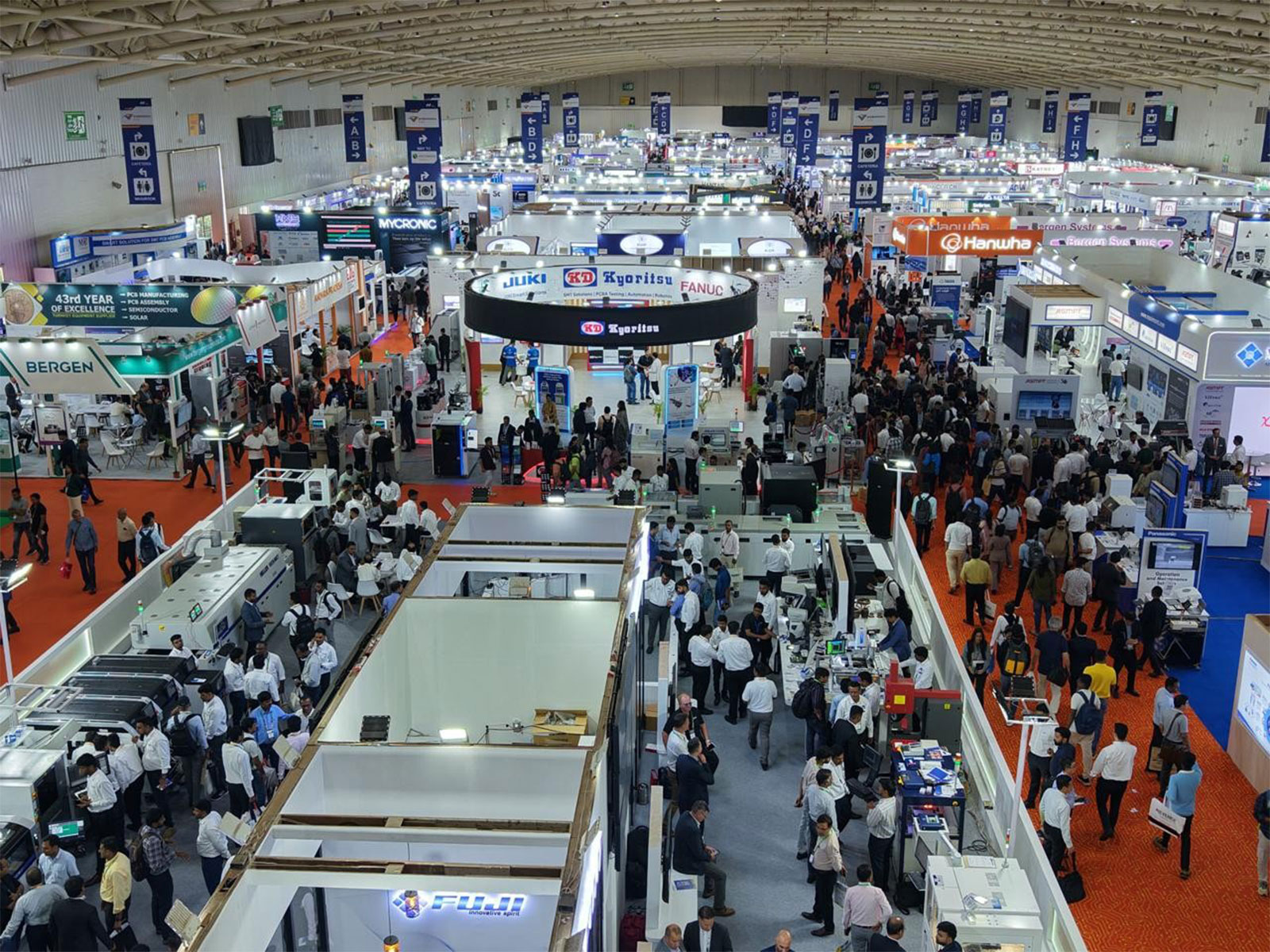
Companies from Germany, China, France, Italy, the United Kingdom, Japan, Israel, the United States, Korea and other markets participated in the Bengaluru edition.
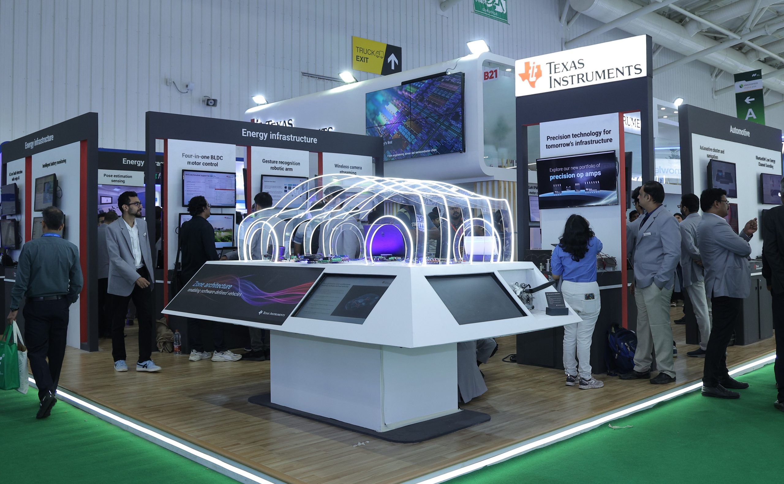
Dedicated pavilions from Germany, Japan, Taiwan and China brought together technologies and suppliers from their respective electronics industries. The Japan Pavilion was organised in partnership with the Japan External Trade Organization (JETRO), while the Taiwan Pavilion was presented with the Taiwan Electrical and Electronic Manufacturers’ Association (TEEMA).
Rather than serving only as international showcases, the pavilions enabled participating companies to hold direct discussions with Indian buyers, understand local manufacturing requirements and explore potential commercial relationships.
Dr. Reinhard Pfeiffer, CEO, Messe München GmbH, said, “Global electronics companies are increasingly in need of a closer understanding of India’s manufacturing requirements and business environment. The Bengaluru edition gave international suppliers direct access to the companies investing in production, sourcing and technology adoption. For Indian participants, it provided an efficient way to compare the capabilities of several established technology markets.”
Conference discussions examine the foundations of competitive manufacturingThe accompanying programme moved the industry conversation beyond manufacturing volume to the capabilities required for long-term competitiveness.
The India Electronics Conclave comprised 14 conferences at the BIEC Conference Centre. Across the event, approximately 150 speakers participated in 18 supporting programmes covering electronics policy, capital goods, artificial intelligence, exports, free trade agreements, printed circuit boards, flexible electronics, standards, compliance and power electronics.
The programme included the eFuture Conference with Avanteum as Knowledge Partner, CEO Forum with ELCINA, Industrial Electronics & Capital Goods Summit 2026 with ICEA, Exports and FTAs: Electronics Sector with MEDEPC, Bharat PCB Tech Conference with ELCINA, VDMA Symposium and OE-A Symposium on Flexible Electronics.
Reinforcing its role as a platform for industry dialogue and future-focused thinking, electronica India and productronica India 2026 hosted the launch of MMI and Avanteum Advisors’ e-paper, eFuture 2035: Engineering India’s Next Electronics Revolution. The report outlines the strategic shifts and opportunities that could shape India’s electronics manufacturing and its position in the global value chain over the next decade.
Technical learning was addressed through the IEEE Standards Workshop on EMI/EMC Compliance and the Power Electronics & Power Supply Design Workshop.
“India’s electronics industry is entering a phase where competitiveness will be measured by consistency, reliability, process maturity and the ability to meet global customer expectations. Forums at electronica India and productronica India 2026 helped bring sharper attention to these priorities by connecting industry leaders, technology providers and policy stakeholders around the practical capabilities required to move from capacity creation to globally competitive manufacturing,” said Rajoo Goel, Secretary General, ELCINA.
The Industrial Electronics & Capital Goods Summit 2026, organised with the India Cellular & Electronics Association, examined the role of domestically available equipment and production technologies in supporting manufacturing growth.
Shri Pankaj Mahindroo, Chairman, India Cellular & Electronics Association (ICEA), said: “As India’s electronics manufacturing ecosystem continues to expand, reliable access to advanced equipment, automation, testing and quality-control technologies will be critical to sustaining growth. The summit provided an important platform for industry and policymakers to examine these requirements from the perspective of real-world production needs and identify the areas where India’s capital-goods and technology ecosystem must continue to evolve.”
The OE-A Symposium brought international and Indian experts together to consider the commercial potential of flexible and printed electronics across mobility, healthcare, energy, consumer products and industrial applications.
Sandip Roy, General Manager, VDMA India, said, “The opportunity in flexible electronics depends on connecting research and technology development with viable industrial applications. The symposium created a useful exchange between international specialists and Indian stakeholders exploring how these technologies can move towards adoption and commercial deployment.”
Speakers participating in the supporting programme said that the value of the discussions lay in bringing policy, manufacturing experience and technical expertise into the same forum.
“The session provided an opportunity to examine the emerging power paradigm in the context of the decisions manufacturers are making today. The discussion highlighted the immediate challenges facing the industry, while also bringing into focus the technologies and capabilities that need to be developed to meet the evolving demands of power electronics over the coming years,” said Amit Kumar, Vice President & Business Unit Head – Metering and Protection Systems, Schneider Electric India.
“India has a significant opportunity to strengthen its position in next-generation PCB design to manufacturing, but realising this potential will require closer collaboration among industry, government, academia and technology providers. The event brought these stakeholders together for a practical and meaningful exchange of perspectives on bridging the journey from design to manufacturability,” said Savita Ganjigatti, Sr. Vice President – Engineering & Operations, Sienna ECAD Technologies (An Avalon Group Company), during the session Engineering for Tomorrow: Design to Manufacturing.
Emerging engineers work on industry-defined challengesThe 2026 edition also introduced formats designed to connect emerging technical talent with practical industry problems.
Organised with HackCulture and supported by presenting partner DigiKey, the electronica India Tech Challenge featured a prize pool of ₹5 lakh. Participating teams developed responses to defined technology challenges and presented their work during the Hackathon Demo Day, where the three winning teams were recognised for the originality, technical merit and practical relevance of their solutions.
The AI Buildathon, conducted by Sarvam AI, and AI Masterclass conducted by GrowthX, explored the application of artificial intelligence to practical use cases. A Hand Soldering Skill Test brought attention to production skills at the operator level, while an industrial visit to the Central Manufacturing Technology Institute provided exposure to an established manufacturing and engineering environment.
At electronica India 2026, the Taipei Computer Association and IIIT-Bangalore signed an LoI to advance Taiwan–India collaboration across AI, electronics, smart manufacturing, smart cities and cybersecurity.
Together, these initiatives connected the event’s wider manufacturing agenda with engineering skills, applied problem-solving and future workforce requirements.
‘India’s Powerplay in Electronics’ reaches the industry nationwideThe Bengaluru edition was presented under the theme “India’s Powerplay in Electronics.” Cricket icon KL Rahul served as Brand Ambassador for the visitor campaign, which ran across outdoor, digital and print media through September 2026. At the event, the campaign shifted from a public-facing message to a physical demonstration of the breadth of companies, technologies and expertise in India’s electronics industry.
Exhibitors and buyers report focused business engagementExhibitors highlighted the quality of conversations with manufacturers, sourcing teams and technology decision-makers attending the Bengaluru edition.
“productronica India 2026 gave us a strong platform to showcase advanced technologies with our global partners. Unveiling Fuji’s CLT-FG for the first time outside Japan was the main highlight. The strong industry response reinforced the growing demand for advanced manufacturing solutions in India and opened new opportunities for collaboration,” said Soni Saran Singh, Founder, MD & CEO, NMTronics India Pvt. Ltd.
“India’s electronics ecosystem is evolving rapidly, with growing focus on technology adoption, local manufacturing and stronger supply chains. The exhibition enabled meaningful conversations around these priorities and how we can support customers across the electronics value chain, from design to delivery,” said Haresh Abichandani, Managing Director, Millennium Semiconductors.
“Visitors came with defined requirements and a clear understanding of the capabilities they wanted to evaluate. This allowed our discussions to move quickly from general enquiries to applications, technical specifications and potential projects,” said Nandini Balasubramanian, Director, Tescom Pvt. Ltd.
Buyers valued the opportunity to compare suppliers and technologies against specific production and sourcing requirements.
“We attended the exhibition with clearly defined requirements for passive components used in electronic control boards. The event provided an excellent opportunity to meet multiple relevant suppliers under one roof, enabling us to compare their technical capabilities, product offerings, quality standards, and application expertise. The interactions were valuable in identifying potential suppliers for further technical evaluation and future collaboration,” said Jagadeesha M H, Team Lead, R&D, Delta Electronics India Pvt Ltd.
“Our priority was to understand which technologies could support improvements in production/quality/testing/automation. The live discussions gave us information that would have taken considerably longer to gather through individual supplier meetings,” said Venkata Ravindra, Head R&D, SFO Technologies.
“The event was the seventh in a row for me. This time, I felt that the combination of Indian and international suppliers gave our team a wider view of the available options. We have shortlisted potential partners and will continue the technical and commercial discussions initiated at the event. It was well organized this time and thanks to the team for making it better every year,” said Anil Krishna K S, Associate Director – Procurement & Supply Chain, Pioneer India Electronics Pvt Ltd.
The trade fairs were supported by the Government of Karnataka, with ELCINA as Partner Association and ICEA as Industry Partner. ELCIA, CLIK, GEZIA and AIEA participated as Supporting Associations; MEDEPC and CEAMA as Strategic Partners; and VDMA, IEEE and OE-A as Conclave Partners.
Yeemak and Delvitech were Gold Partners, while Mouser Electronics participated as Registration Partner. JETRO and TEEMA supported the Japan and Taiwan pavilions, respectively.
Expanded national format proceeds to Delhi-NCRThe conclusion of the Bengaluru edition completes the first year of the trade fairs’ expanded national model.
Previously conducted in alternate years in Noida and Bengaluru, electronica India and productronica India moved to annual editions in both markets in 2026. The change represents 50 percent growth under the new format and provides more regular access to the electronics manufacturing regions of northern and southern India.
The next edition will be held from 28–30 April 2027 in Delhi-NCR.
The programme will mark the launch of Defence Electronics NEXT, creating a dedicated platform for technologies, capabilities and partnerships supporting India’s defence electronics ecosystem. It will also maintain a strong focus on printed circuit boards through BPCA and on the semiconductor value chain through the India Semiconductor Conclave.
Supported by the Uttar Pradesh Host State Partnership, these initiatives align with the Government of Uttar Pradesh’s investment priorities in defence electronics, PCBs, semiconductors and advanced manufacturing. Together, they will connect industry, government and technology stakeholders around sectors critical to India’s electronics manufacturing ambitions.
The post Electronica India and Productronica India 2026 Conclude in Bengaluru with 793 Exhibitors and 52,411 Business Visitors appeared first on ELE Times.
AI Vision Assistant Pendant for the Visually Impaired
A wearable pendant helps visually impaired people understand what is around them. When a button is pressed, an ESP32-CAM takes a photo of the environment, sends it to the cloud to get a text description, converts it to speech, and plays it through a speaker. The project is by Anand D and overcomes the limits of traditional canes with proximity sensors, which only detect nearby obstacles.
The central board is the ESP32-CAM, which combines a camera and a microcontroller in a compact module. The user presses a limit switch to capture the image. The photo is sent to the CircuitDigest Cloud, which analyzes it and returns a detailed description in JSON format. The text then goes to Sarvam AI, which converts it into an audio file in Base64 format. Finally, the ESP32-CAM downloads the file, decodes it, and plays it through the I2S MAX98357 amplifier and a speaker.
Components of the pendant and power supplyBesides the ESP32-CAM, only a few components are needed: the MAX98357 amplifier, a speaker, an HW-105 5V boost converter, a limit switch, a button, and a toggle switch. The boost converter powers the entire system from a battery. It must supply an average of 600mA, a value that the ESP32-CAM draws especially during Wi-Fi transmission and audio playback.
The audio sampling frequency is initialized to 16000 Hz, while the AUDIO_GAIN_FACTOR is set to 2.5f to make the volume suitable for listening. An additional button allows changing the response language between Hindi, English, Tamil, and Malayalam. In this way, the device adapts to the user, not the other way around.
The firmware: libraries and API limitsThe source code uses several libraries to handle the camera, connection, and audio. These include esp_camera.h, WiFi.h, HTTPClient.h, driver/i2s.h, and mbedtls/base64.h. ArduinoJson is used for parsing the JSON response. The flow is linear: capture, upload, description, speech synthesis, playback.
There are, however, limits to respect. Sarvam AI, with the Bulbul v3 model, accepts a maximum of 2500 characters per request. This limit is higher than Wit.ai, which stops at 280 characters, and Google TTS, which reaches 5000. In practice, the description generated by the cloud almost always falls within the limit, but the code must handle any responses that are too long.
For those who want to dig deeper into the code, sketches, and assembly details, Anand D’s repository is the right starting point. The project demonstrates how an inexpensive microcontroller can become a real assistive device, using computer vision to describe the environment and speech synthesis to communicate it.
- ESP32-CAM with integrated camera
- I2S MAX98357 amplifier
- 8 ohm speaker
- HW-105 5V boost converter
- Limit switch for capture
- Button for language change
- Toggle switch for power
To program the board, a USB-TTL converter is needed, which allows connecting the ESP32-CAM to a PC. Alternatively, those who want a more modern board can consider the ESP32-C6-Zero development kit, which offers Wi-Fi 6 and a compact format, although it requires an external camera.
Source: https://circuitdigest.com/microcontroller-projects/esp32cam-ai-vision-assistant-pendant
The post AI Vision Assistant Pendant for the Visually Impaired appeared first on Open Electronics.
Tata Electronics Signs Seven MoUs to Strengthen India’s Semiconductor Value Chain
To strengthen India’s semiconductor manufacturing ecosystem across different stages of the value chain, Tata Electronics signed seven Memorandums of Understanding (MoUs) with global companies and Indian institutions during SEMICON India 2026, held in New Delhi from September 17 to 19. The collaborations cover wafer manufacturing, assembly and testing, advanced semiconductor packaging, materials, technology development, supply-chain localisation and talent development.
One of Tata Electronics’ major collaborations is with Nexperia, a Dutch semiconductor company. This partnership covers front end wafer fabrication, back-end assembly, and testing along with technology and ecosystem development. As per the partnership, Nexperia’s semiconductor products are expected to be manufactured and packaged through Tata Electronics’ facilities located in Dholera, Gujarat and Jagiroad, Assam.
Tata Electronics’ second collaboration is with Fujifilm, a Japanese multinational company, with the primary goal of developing a semiconductor materials ecosystem in the Dholera fabrication facility to enhance supply chain resilience. These materials include high-purity process chemicals and raw materials such as photoresists, CMP slurries, and thin-film solutions. Fujifilm plans to invest ₹800 crore to establish a semiconductor materials plant in Dholera to support the localisation of semiconductor materials.
Another important partnership is with Enomoto, a Japanese steel manufacturing company signed with Tata Electrics to strengthen its semiconductor packaging materials supply chain facility in Jagiroad, Assam. Enomoto will support Tata Electronics by providing manufacturing expertise for developing next-generation semiconductor packaging capabilities.
This collaboration of Tata Electronics with global partners reflects the effort to develop an integrated semiconductor ecosystem in India, supporting Tata Electronics’ planned fabrication facility in Dholera and semiconductor packaging facility in Assam while building domestic capabilities across the semiconductor value chain.
The post Tata Electronics Signs Seven MoUs to Strengthen India’s Semiconductor Value Chain appeared first on ELE Times.
Interview | Hitesh Garg, Vice President & India Managing Director, NXP Semiconductors
The automotive industry is making a seamless transition to Software Defined Vehicle (SDV) architectures and technology providers are gearing up for exciting times ahead! In an exclusive interaction with Anwesh Koley of ELE Times, Hitesh Garg, Vice President & India Managing Director, NXP Semiconductors, shared his views on SDVs and their evolution in the automotive landscape. Excerpts from the interview:
ELE Times: With car buyers becoming more concerned with comfort, connectivity, and safety than horsepower and acceleration, how does this impact the design of technological architectures in SDVs?
Hitesh Garg: Traditional automotive engineering focused on mechanical performance, but today’s buyers increasingly evaluate vehicles based on their digital experience. About 95% of Indian consumers are willing to pay for Software-Defined Vehicle capabilities, with safety, security, and continuous vehicle-health reporting emerging as key purchase considerations. As a result, vehicles are evolving into intelligent, software-driven platforms where features can be continuously enhanced throughout their lifecycle.
NXP is powering this transition through its portfolio of automotive processors, secure connectivity, edge AI, radar, and vehicle networking solutions that help OEMs build scalable, software-defined vehicle architectures.
ELE Times: With vehicles becoming increasingly software-defined, share your thoughts on NXP’s advancements in zonal networking solutions.
Hitesh Garg: At NXP, we view zonal networking as one of the foundational building blocks for scalable SDVs. Our S32 portfolio, including the S32G vehicle network processors and S32J family of Ethernet switches, is designed to deliver the secure, deterministic, and high-bandwidth communication required for next-generation architectures.
More recently, we introduced the SAF8444 multi-gigabit Automotive Ethernet switch, enabling higher network bandwidth and lower latency to support data-intensive applications such as advanced driver assistance systems (ADAS), autonomous driving, and immersive in-vehicle experiences. Combined with Automotive Ethernet, Time-Sensitive Networking (TSN), and intelligent gateway capabilities, these solutions enable seamless communication between sensors, actuators, and centralised compute systems.
ELE Times: India is increasingly positioning itself as a design-led electronics ecosystem. In this scenario, please elaborate on NXP’s current initiatives in the development and adoption of Software Defined Vehicles.
Hitesh Garg: India plays a critical role in NXP’s global automotive R&D ecosystem. With more than 2500 employees across our centres, the recent acquisition of Kinara further strengthens NXP’s edge AI capabilities, enabling high-performance neural processing directly within the vehicle for applications such as advanced driver assistance, driver monitoring, and intelligent in-cabin experiences.
Coupled with India’s growing semiconductor ecosystem and supportive government initiatives, we see significant opportunities to collaborate with OEMs and ecosystem partners to accelerate the development of globally competitive SDV solutions.
ELE Times: Software Defined Vehicles require a fundamentally different approach to vehicle architecture. How is the industry poised to address this challenge?
Hitesh Garg: The industry is adopting standardised software platforms, service-oriented architectures, Automotive Ethernet, zonal and centralised processing to simplify integration and improve scalability. Equally important is the growing collaboration between semiconductor companies, OEMs, Tier-1 suppliers, cloud providers, and software developers to reduce development complexity and accelerate time-to-market.
ELE Times: What’s different in the current approach to designing an SDV than 3-to-5 years ago?
Hitesh Garg: Over the last few years, the industry has moved from viewing software as an enhancement to recognising it as the primary driver of vehicle innovation. Three to five years ago, software largely supported individual vehicle functions through isolated ECUs. Today, manufacturers are designing vehicles around centralised computing platforms where software defines functionality, user experience, and feature evolution throughout the vehicle’s lifecycle.
NXP is enabling this shift with our automotive processors, radar solutions, secure connectivity technologies, and vehicle networking platforms designed to support this evolution by enabling scalable compute, real-time intelligence, and continuous software innovation while meeting the stringent safety and cybersecurity requirements of modern vehicles.
ELE Times: Software seems to be enabling more variations. Are there any engineering challenges in managing and implementing this?
Hitesh Garg: The increasing software content in vehicles brings tremendous flexibility, but it also introduces new engineering challenges around functional safety, cybersecurity, software integration, and lifecycle management. As vehicle architecture becomes more centralised and software-driven, ensuring that hardware and software operate reliably, securely, and in compliance with automotive safety standards becomes critical.
ELE Times: What can automotive engineers do to balance the need for more circuitry with the requirement to limit weight, particularly in EVs?
Hitesh Garg: One of the most effective ways to achieve this is by transitioning from distributed ECU architectures to centralised and zonal architectures. Instead of connecting every sensor and actuator through long wiring harnesses, zonal architectures group components based on their physical location within the vehicle and connect them through high-speed Automotive Ethernet. This significantly reduces cable length, lowers vehicle weight, simplifies manufacturing, and improves serviceability while supporting future software-defined capabilities.
Equally important is semiconductor integration. By consolidating multiple functions into high-performance processors and highly integrated system-on-chip (SoC) solutions, OEMs can reduce component count, optimise power consumption, and improve thermal efficiency.
ELE Times: What are the barriers to SDV adoption, and what can OEMs and technology providers do to address these concerns?
Hitesh Garg: Infrastructure is an important enabler for SDVs. The deployment of reliable infrastructure, high-speed connectivity, and intelligent transport systems will also be essential to unlock the full potential of SDVs. Addressing these challenges requires close collaboration across the automotive ecosystem. Semiconductor companies, OEMs, Tier-1 suppliers, software developers, and standards bodies must work together to build interoperable platforms based on open architectures and common software frameworks.
ELE Times: How do you perceive the future of connected car technology and what innovations can we expect in the foreseeable future?
Hitesh Garg: We at NXP are enabling this future through our broad automotive portfolio spanning secure connectivity, V2X, UWB, radar, edge AI, and high-performance automotive processing. As vehicles become more software-defined and connected, our focus remains on delivering secure, scalable technologies that enable automakers to accelerate innovation while ensuring functional safety, cybersecurity, and reliability. For India, where connected mobility is gaining momentum alongside the growth of electric and software-defined vehicles, this presents a significant opportunity to develop globally competitive solutions that shape the future of intelligent transportation.
ELE Times: What are your views on the India Semiconductor Mission 2.0?
Hitesh Garg: Government initiatives such as ‘ISM 2.0’ are a defining milestone in India’s journey toward global semiconductor leadership. By expanding support across the entire value chain from manufacturing and advanced packaging to critical materials and design, this initiative builds a foundation for long-term competitiveness.
India’s world-class engineering talent is a proven asset, and sustained R&D investments will further elevate its position in the global supply chain. At NXP, we are fully committed to this vision. We continue to advance cutting-edge R&D locally and nurture future-ready talent. We believe that collaborative ecosystem innovation is the key, and we look forward to partnering with industry, academia, and policymakers to drive India’s emergence as a global semiconductor hub.
The post Interview | Hitesh Garg, Vice President & India Managing Director, NXP Semiconductors appeared first on ELE Times.
ICEA Drives India–Malaysia Semiconductor and Electronics Industry Collaboration at SEMICON India 2026
India Cellular & Electronics Association (ICEA) along with the High Commission of Malaysia and Malaysia External Trade Development Corporation (MATRADE) organized the India-Malaysia Semiconductor & Electronics Industry Collaboration: Strategic Business, Investment & Partnership Opportunities in India at SEMICON India 2026, held at Yashobhoomi, New Delhi to facilitate discussions among Indian and Malaysian industry members to build on synergies and scale in business, investment, and technology collaboration.
The engagement covered key areas including semiconductors, OSAT/ATMP, semiconductor equipment, inspection and metrology, automation, electronics manufacturing and advanced technologies. Participating companies discussed their capabilities, requirements and potential areas for partnerships and investment.
Ms Shamilah Perumal, Minister (Economic Affairs), High Commission of Malaysia, highlighted Malaysia’s established semiconductor and electronics ecosystem and the potential to build stronger linkages with India’s rapidly expanding semiconductor design, manufacturing and electronics ecosystem.
The programme also brought an important state-level investment perspective through the participation of Ms. Pallavi Verma, IAS, Executive Director, Guidance Tamil Nadu, and Shri Alok Kumar, Principal Secretary, Department of IT & Electronics, Government of Uttar Pradesh. They highlighted investment opportunities, policy initiatives, incentives and facilitation mechanisms available to companies.
The engagement was further strengthened by the participation of Ms. Siti Nur Nafhatun, MATRADE, in the second industry interaction session, with Dr. Neeraj Agarwal, ICEA, coordinating the industry interactions and facilitating focused discussions between the participating Indian and Malaysian companies.
Pankaj Mohindroo, Chairman, ICEA, said: “India and Malaysia have complementary strengths across the semiconductor and electronics value chain. Malaysia has built significant capabilities in semiconductor manufacturing, packaging and related technologies, while India is rapidly expanding its capabilities across design, manufacturing, components and electronics production. The opportunity is to connect these strengths through investments, technology partnerships, manufacturing linkages, joint R&D and potential joint ventures. Such industry-led engagement can create stronger and more resilient regional value chains.”
The discussions also explored collaboration beyond the immediate semiconductor and electronics ecosystem, including Quantum Technologies, Rare Earth Elements & Magnets, AgriTech and other emerging technologies, creating potential avenues for joint research, technology development and investment.
ICEA will continue to engage with global industry, governments, investment agencies and technology ecosystems to facilitate meaningful business connections and support investments, technology partnerships and deeper integration of India into global electronics and semiconductor value chains.
The post ICEA Drives India–Malaysia Semiconductor and Electronics Industry Collaboration at SEMICON India 2026 appeared first on ELE Times.
LEDs for under-cabinet illumination upgrades

Long life? Power efficient? Color temperature flexibility? Drop-in replacement? Yes please, I’ll take one of these!
I’ve long pontificated in various blog posts and teardowns about the transformative effects of LED-based lighting. LEDs improve existing illumination systems beyond what was possible with legacy incandescent (including halogen), fluorescent and other technologies, such as with vehicle headlights. They also, courtesy of their combination of inherent low power consumption and heat dissipation plus a leverage of DC voltage sources, enable new classes of products previously not possible, such as in networked “smart” lighting systems, light bulb-shaped security cameras and luminaires with embedded backup batteries.
Personally, I’ve to date mostly used them to replace incandescent bulbs of various shapes and sizes, as well as to upgrade bulb-shaped CFLs. But I recently had an idea that thankfully panned out perfectly. When my wife and I moved into our home more than a decade back, there already was an under-cabinet light source above the desk in the kitchen, AC-fed and controlled by a single-pole wall switch. Judging from its appearance, I’m guessing it’d been there since the home’s mid-1980s initial construction. It wasn’t exactly aesthetically attractive (and I’m being kind in wording it this way), although given its installation location, I mostly only saw the light it emitted, not the light itself.

So, in the spirit of “If it works, don’t touch it”, I long settled for leaving it alone. The problem was, though, that I couldn’t not touch it. Illumination came from a horizontally arranged combo of 12” and 21” fluorescent tubes, each of which regularly needed to be replaced (each time preceded by an annoying flickering pending-demise alert). Less frequently, but still more often than I’d prefer, one or both increasingly-difficult-to-source starters would fade to black, necessitating swap(s), too. And even when the fluorescent light was working normally, its humming transformers were enough to drive a sane person crazy (I’m arguably sane, anyway).
Conventional successors miss the markI could have just ripped it out (which, as you can already tell by the earlier photo, I eventually did) and replaced it with a conventional LED-based light “strip”, like one of these or the one above my work bench downstairs, which works great and is even metal frame touch-controllable for on/off purposes.

But in my kitchen application, it’s conversely non-ideal. First off, it requires tether to a separate “wall wart” to handle AC/DC conversion. That wall wart needs to be plugged into an outlet somewhere; unfortunately, the one at the desk is already at “full employment”. Then there’s the unsightly wire running between the wall wart and light, feeding DC power from the former to the latter. Yes, battery-operated LED strip light versions exist, too, but that’s where my “don’t touch it” aspiration comes in again. Those batteries inevitably get exhausted and need to be replaced. The whole point here is to just “set it and forget it”.
Touch leads to the other twist. Some of these conventional LED strip lights embed power switches somewhere on the plastic or metal assembly. Others, like the one downstairs, offer touch control as already mentioned. But in either case, you need to operate the successor differently than previously done with the original fluorescent unit. Remember that wall switch? It’ll still be sitting there. Won’t it get lonely if it’s no longer in use? And won’t I go slowly mad (or madder than I already am) every time I flip it, leveraging muscle memory, and then remember it’s no longer hooked up?
Form, fit, and function in the kitchenBut, after doing a bit more online research and shopping, I finally came across exactly what I was looking for. Behold NICOR Lighting’s 33” LED Direct Wire Under Cabinet Light.

When I bought mine at the beginning of July, it was nearly $53 brand new (and $43 and change in open-box condition) on Amazon. Now, as I write this, it’s only $38.70 brand-new. And so it goes. It was a tad bit shorter than its predecessor, length-wise (as well as quite a bit narrower in both width and height), but I was still able to leverage the existing mounting holes. And again, since I mostly see the light emitted, not the light itself, the dimensional variance was no biggie.
Here are some more stock photos.


You may have already noticed from them, for example, that an integrated power switch is optional; for aforementioned reasons, I didn’t buy that variant (although I could have just kept it switched on all the time, still relying solely on the wall switch). The key innovation is that the AC/DC conversion block is built in; it’s fed by the same AC wiring conduit used by its precursor. And if your wall switch is dimmable (mine’s not), it’s apparently compatible with those, too.

You may have also already noticed that it has color temperature customization control, via a five-position switch.


There are 56 two-LED clusters across its total under-cabinet span.

Moving the switch from one position to another varies which LED(s) in each cluster is/are powered, along with their relative intensity. The LED lights in my office work the same way.

All in all, I’m a happy customer (with, as always, no personal affiliation with the company, mind you). I’m left with only two things to wonder about:
- How long will it take for the first LED to fluorescent-reminiscent flicker, and then die?
- And, with reminiscent visions of Christmas Tree lights dancing in my head, will it take down the rest of the LED strip with it?
Place your bets, and more generally share your thoughts, in the comments.
—Brian Dipert is the associate editor, as well as a contributing editor, at EDN.
Related Content
- LED light bulb manufacturers diversify in search of sustainable profits
- LED headlights: Thank goodness for the bright(nes)s
- Dissecting incandescent-reminiscent stealth security
- Dissecting a battery-backed LED light bulb
- A failed switch in a wall plate = A garbage disposal that no longer masticates
The post LEDs for under-cabinet illumination upgrades appeared first on EDN.
Сторінки



