


Feed aggregator
Keysight and Sateliot Selected by European Space Agency to Develop Blockchain‑Enabled Framework for 5G Non‑Terrestrial Networks
Keysight Technologies, Inc. has been selected by the European Space Agency (ESA)
to lead a three‑year development program focused on creating secure, blockchain‑enabled
anomaly detection for 5G non‑terrestrial networks (NTN). Keysight will serve as the prime
contractor, collaborating with Sateliot to support key technical development and satellite mission
integration.
As more satellite communication constellations are deployed, space‑based networks are
becoming increasingly complex, with growing interactions between satellites, ground systems,
and terrestrial 5G infrastructure. This introduces new challenges related to quality of service,
anomaly management, operational security, and confidence in network behavior once deployed.
Looking ahead to 6G, where non-terrestrial infrastructure will play a central role, ensuring
access to trusted, verifiable data will be critical to enabling autonomous and artificial intelligence
(AI)-driven network operations.
The project, which benefits from the support of ESA’s Space for 5G/6G & Sustainable
Connectivity program line within the Agency’s Advanced Research in Telecommunications
Systems (ARTES), is designed to address these challenges by establishing a secure, verifiable
trust framework for NTN environments. Keysight will leverage its design, test, and measurement
expertise to explore how blockchain, AI, machine learning (ML), and digital calibration
certificates can be applied across the full NTN lifecycle, from satellite manufacturing and
calibration to in‑orbit operation and service delivery.
Albert Pujol, Chief Innovation Officer at Sateliot, stated: “This program represents a
definitive shift toward integrating space-based assets into a secure, unified 5G ecosystem. By
anchoring blockchain within our orbital operations, we are creating a transparent validation layer
that allows massive IoT networks to scale globally while consistently ensuring security and
performance.”
Antonio Franchi, Head of the Space for 5G/6G & Sustainable Connectivity programme at
ESA, said: “The future of Europe’s connectivity depends on networks that are not only
advanced, but trusted, resilient and secure. Supporting this project, which benefits from
Keysight’s leadership and Sateliot’s expertise, underscores ESA’s commitment to helping
pioneer the technologies required to safeguard the integration of non-terrestrial and terrestrial
networks. Together, we’re not only taking a step towards defending Europe’s communications
against spoofing and tampering, but we’re also ensuring that our Member States remain at the
forefront of secure 5G and future 6G communications.”
Eric Taylor, Vice President, Aerospace, Defense and Government Solutions at Keysight,
said: “This initiative represents a major step toward securing hybrid space–terrestrial networks
at a time when global NTN deployments are accelerating. By combining test and measurement
expertise with AI-driven assurance and blockchain technologies, this work will demonstrate how
trust can be embedded across the full NTN lifecycle – from design and validation through in-orbit
operation.”
By integrating these technologies, the program aims to enhance the integrity and reliability of
space‑based IoT, 5G, and future 6G communications, helping to protect networks from
spoofing, tampering, and other cyber threats. Over the course of the program, development will
progress from laboratory research and prototyping to a full in‑orbit demonstration, validating
how blockchain‑anchored trust, autonomous anomaly detection, and secure telemetry can be
applied in operational satellite environments.
The ESA‑funded program is expected to inform future NTN operations, strengthen Europe’s
position in secure satellite connectivity, and accelerate the adoption of trusted space‑based
5G/6G networks worldwide.
The post Keysight and Sateliot Selected by European Space Agency to Develop Blockchain‑Enabled Framework for 5G Non‑Terrestrial Networks appeared first on ELE Times.
BluGlass secures AUS$1.4m Phase II contract under JDA with Uviquity
КПІ ім. Ігоря Сікорського — серед лідерів Консолідованого рейтингу закладів вищої освіти України 2026!

Інформаційний освітній ресурс «Освіта.ua» оприлюднив Консолідований рейтинг закладів вищої освіти України 2026, у якому КПІ ім. Ігоря Сікорського вкотре підтвердив свої лідерські позиції:
WeEn launches 1200–2300V silicon carbide power modules
Temporary workbench set up at a university dorm
 | submitted by /u/BlownUpCapacitor [link] [comments] |
I just reorganized and labeled my components
 | Ignore the rock drawer I didn't have a better place for my cool rocks [link] [comments] |
Rad-hard gate driver enables GaN adoption

Infineon’s RIC70115 GaN HEMT gate driver provides the radiation hardness and long-term reliability required for satellite and space applications. Supporting both silicon FETs and GaN HEMTs in low-side and high-side configurations, the device helps ease the transition from silicon to GaN.

Operating over a temperature range of -55°C to +125°C, the RIC70115 is characterized for single-event effects up to a linear energy transfer (LET) of 81.9 MeV·cm²/mg and a total ionizing dose (TID) of up to 100 krad(Si). Its independent Miller clamp prevents parasitic-induced turn-on while maintaining switching speed, reducing switching losses. Truly differential input logic rejects common-mode noise and minimizes the effects of EMI and RFI.
An integrated low-dropout regulator generates a tightly regulated 4.8-V drive voltage from a 5-V or 12-V source, supporting a supply voltage range of 4.75 V to 15 V. The RIC70115 provides a 1.5-A source current and a 2.5-A sink current, with propagation delay matching of up to 2.9 ns.
The RIC70115 is offered in a hermetically sealed 16-pin LCC package or in die form.
The post Rad-hard gate driver enables GaN adoption appeared first on EDN.
Holotomography system analyzes glass defects

Tomocube’s HT-T1D is a desktop holotomography system for high-resolution, non-destructive 3D defect analysis of glass substrates used in semiconductor packaging. It images internal defects and other fine features with a lateral resolution of 161 nm and an axial resolution of 1.298 µm.

Glass core substrates and glass interposers are gaining traction as key enabling materials for AI accelerators, high-bandwidth memory, and other advanced packaging applications. Manufacturers need to identify the root causes of micro-defects and quickly translate inspection data into process improvements.
The HT-T1D system applies visible-light holotomography to visualize the three-dimensional refractive-index distribution inside glass with refractive-index sensitivity down to ~10⁻⁴ Δn. Its non-destructive measurements enable repeated analysis of the same location across successive process stages, allowing users to track when and how defects form, propagate, or enlarge.
When conventional in-line panel inspection tools such as automated optical inspection (AOI) systems flag a potential defect, the HT-T1D uses the corresponding coordinates to reconstruct the interior of the glass substrate in three dimensions. It resolves the defect’s location, morphology, and depth profile that surface inspection alone cannot reveal.
The post Holotomography system analyzes glass defects appeared first on EDN.
TVS diodes clamp automotive transients

Two TVS diode series from Littelfuse, the TP5.0SMD-FL and TP1KSMB-FL, protect 48-V automotive electronics from voltage transients. Based on the FlatSuppressX TVS architecture, the devices exhibit a flatter clamping characteristic with a significantly lower clamping voltage than conventional TVS components. Their foldback/snapback function tightly controls transient response while avoiding latch-up risk.

The TP5.0SMD-FL series has a peak pulse power rating of up to 5 kW in a DO-214AB (SMC) package. The TP1KSMB-FL series has a peak pulse power rating of up to 1 kW in a DO-214AA (SMB) package. Devices in both series are AEC-Q101 qualified, providing scalable protection options for varying system requirements. Their architecture enhances system efficiency, enabling the use of lower-rated downstream components.
Optimized for protecting I/O interfaces, power buses, and other vulnerable circuits in automotive electronics, particularly 48-V architectures, these TVS diodes provide a fast transient response, typically in less than 1 ps.
The TP5.0SMD-FL and TP1KSMB-FL series are available in tape and reel format in quantities of 3,000. Sample requests are accepted through authorized Littelfuse distributors worldwide.
The post TVS diodes clamp automotive transients appeared first on EDN.
Microchip offers free MPLAB compilers, AI tools

MPLAB XC Pro Compilers and the MPLAB Machine Learning Development Suite from Microchip are now available at no cost. Unlimited installations give users free access to advanced optimization capabilities and integrated embedded machine learning workflows, whether working individually or as part of a development team.

Previously available through paid license tiers, the MPLAB XC Pro Compilers reduce code size, lower memory usage, improve execution speed, and generate architecture-optimized code for embedded applications. These capabilities support software development across Microchip’s 8-bit, 16-bit, and 32-bit MCU and MPU portfolio.
The MPLAB Machine Learning Development Suite includes the Model Builder plug-in for MPLAB X IDE and Microsoft Visual Studio Code. It generates optimized AI and IoT sensor recognition code to support embedded machine learning development on resource-constrained devices.
MPLAB XC Compilers and the MPLAB Machine Learning Development Suite are now available as free, unrestricted-use downloads.
The post Microchip offers free MPLAB compilers, AI tools appeared first on EDN.
RDIMM chipset boosts server memory bandwidth

The Rambus DDR5 9600 server RDIMM chipset supports DDR5 RDIMMs operating at up to 9600 MT/s in CPU-based server platforms. The chipset is built around the RCD06 sixth-generation registering clock driver, which increases bandwidth by 20% over the previous generation. As a key control-plane chip, the registering clock driver distributes command/address, chip-select, and clock signals to the DRAM devices on the RDIMM.

In addition to the RCD06, the chipset includes the PMIC5030 power management IC and a serial presence detect (SPD) hub with an integrated temperature sensor. The SPD hub communicates via the I3C bus for system configuration and thermal management. Two dedicated temperature sensors per DIMM provide precision thermal sensing and, in combination with the SPD hub, enable three points of thermal telemetry for the memory module.
By integrating clocking, control, and power management functions, the chipset helps ensure signal and power integrity at high data rates while simplifying the design of DDR5 RDIMMs. This level of integration becomes increasingly important as server architectures scale to support higher processor core counts, larger memory capacities, and the sustained demands of continuously running AI workloads.
Learn more about the DDR5 9600 Server RDIMM chipset here.
The post RDIMM chipset boosts server memory bandwidth appeared first on EDN.
Vector Photonics developing packaging to speed adoption of PCSELs
NextGO Epi raises €2m in pre-seed funding
Infineon introduces rad-hard GaN HEMT driver
[Workbench Wednesday] My favorite place to be out of anywhere
![[Workbench Wednesday] My favorite place to be out of anywhere](https://preview.redd.it/ymg6hx71jfdh1.png?width=140&height=105&auto=webp&s=9675d84a98f3a5c357c03dadf5dcf40cfa728548 "[Workbench Wednesday] My favorite place to be out of anywhere") | submitted by /u/holysbit [link] [comments] |
Holux GR-213 GPS USB to serial mod
 | I have a couple of these receivers I got in a pile of old stuff and by defuse they're USB but I wanted to use them with my microcontrollers, so I ripped one apart with a simple pry tool then removed the pressed on RF shield to expose the goodies. Looking at the USB to serial transceiver, I see it's a PL-2303HX and looking at the datasheet, pin 1 is serial TX and pin 5 is serial RX, so I traced them to two open solder bridges. Closing those to solder bridges with questionable soldering using an oversized tip resulted in the two unused pins now making connection I decided to use the existing cabling so I used a small pry tool to lift up the plastic tab holding the green and white USB data wires and pulled them out and inserting them into their new homes After snipping off the USB connector, red to +5v, black to negative, and the two serial lines to my ESP32 pins, I started streaming NMEA datagrams over uart ❤️ NOTE: the default speed for this receiver is 4800bps [link] [comments] |
Deep physics, materials science enhance dielectrics, varactors

When doing analog design, especially at higher frequencies ranging into the microwave region, it’s normal to focus on devices and the performance they enable in the specific topology. But there’s another aspect of microwave design that’s important to keep in mind: the role of advanced materials and the atomic-scale physics that allows conception, construction, and test of the advanced devices need to reach toward the multi-gigahertz part of the spectrum.
This is demonstrated by a recent Cornell University-led development related to voltage-tunable capacitors, or varactors, that combine high performance with low loss—and the road to get there. Traditional varactor technologies, while effective, often hit a performance ceiling due to intrinsic material limitations, particularly when it comes to dielectric losses that degrade signal quality.
A federal research program was initiated in 1999 to find materials for varactors that would offer lower dielectric losses at higher frequencies. The “back story” of success here is yet another example of how progress is often not linear, predictable, or obvious, despite the way it’s often portrayed.
The research team’s success here is due to persistence and following a very different path, as the project has been a long journey. While nearly every scientific team in the program focused on using barium strontium titanate, the Cornell team looked at layered crystalline materials, a type of perovskite structure known as Ruddlesden-Popper thin films, characterized by their exceptionally low energy loss at microwave frequencies.
Unfortunately, these films also had a major drawback: according to the accepted understanding of their crystal symmetry, they shouldn’t have been able to provide the tunability needed for practical devices.
A member of the research team was developing a new technique for measuring the dielectric properties of thin films across a wide range of frequencies. One of his measurements of strontium titanium oxide with composition Sr4Ti3O10, a layered Ruddlesden-Popper thin film, suggested something remarkable: the supposedly untunable material might, in fact, be tunable after all.
But there was a problem: the effect only appeared in an in-plane geometry, in which the electric field moved sideways through the material. Real-world devices such as voltage-tunable capacitors used in microwave circuits generally require an out-of-plane design, in which the electric field moves vertically through the film, enabling smaller, more efficient components.
Researchers spent a decade trying to find a way to preserve their low microwave loss while making them more tunable and more practical. They then asked a more radical question: what if they could change the symmetry of the material itself? If so, it might be possible to change the symmetry in a specific family of Ruddlesden-Popper compounds made from barium, strontium, titanium, and oxygen.
In a true multi-institution effort with collaborators at Cornell, the University of Connecticut, Rice University, the University of Maryland, Boise State University and the National Institute of Standards and Technology (NIST), they engineered a new version of the material by inserting carefully spaced rock-salt layers. The strategy effectively rewrote the material’s internal rules, allowing it to exhibit the out-of-plane behavior needed for practical devices while preserving the low-loss characteristics that had made the Ruddlesden-Popper thin films attractive in the first place.
By engineering a film structure that introduces a unique rock-salt atomic layer interleaved with every “n” perovskite unit cell, the researchers created a new class of thin films whose symmetry properties could be precisely controlled (Figure 1).

Figure 1 Researchers used advanced microscopy to confirm the atomic structure of an engineered Ruddlesden-Popper material. The diagrams show how alternating layers in the crystal helped produce the material’s unusual combination of tunability and low energy loss. Source: Cornell University
From possible breakthrough to despair, then to a solution
But this success led to another dead-end, as the new out-of-plane devices posed an entirely different metrology problem. The frequencies most relevant for modern communications systems are among the most difficult to measure accurately because at those high frequencies, the signal from the material can be distorted by the test structure itself—the metal electrodes, wiring, and geometries surrounding the dielectric. So, when the researchers first tested the new Ruddlesden-Popper devices at microwave frequencies, the results were confusing.
Addressing this issue, a NIST-based group began to develop a new metrology approach capable of characterizing the material in an out-of-plane, metal-insulator-metal capacitor geometry at frequencies beyond the reach of conventional techniques. They added a “control structure” using a sheet of metal that had the same topology as the device. Measuring that control structure let the team perform an additional round of calibration, subtracting away distortions caused by the test structure itself, and isolating the dielectric’s true microwave response (Figure 2).

Figure 2 The microwave measurement setup used by the NIST team in Boulder, Colorado. Source: NIST via Cornell University
Their custom-tailored composition exhibits a remarkable relative tunability of 51% under an applied electric field of 250 kV/cm, which is almost double the performance of many conventional tunable dielectrics. At the same time, it maintains an impressively low dielectric loss that translates to a material quality factor of about 200. For the best version, the measured dielectric tuning figure of merit (FOM) showed tenfold improvement for out-of-plane tunable dielectrics at 10 GHz.

Figure 3 Various perspectives on microwave characterization are displayed at ambient temperature. Source: Cornell University
Will this lead to new varactors that you can buy? Obviously, it’s too early to say; there are still many potential obstacles on the path to commercialization, if it even happens.
But I do think the right screenwriter could make an exciting story out of this long quest with its advances, insight, contrary thinking, roadblocks, and eventual success. It would be nice to see a true story of science discovery and innovation captured and brought to a more general audience (can you think of any recent ones other than the 2023 blockbuster movie Oppenheimer?).
The work is detailed in their intense paper with a deceptively simple title “Breaking symmetry yields a low-loss out-of-plane tunable microwave dielectric” published in Nature Electronics; while that paper is behind a paywall, a “student” preprint copy is posted at ResearchGate here. In addition, there’s a fairly technical yet very readable description of the work posted at Bioengineer.org (why there—I can’t say).
Bill Schweber is a degreed senior EE who has written three textbooks, hundreds of technical articles, opinion columns, and product features. Prior to becoming an author and editor, he spent his entire hands-on career on the analog side by working on power supplies, sensors, signal conditioning, and wired and wireless communication links. His work experience includes many years at Analog Devices in applications and marketing.
Related Content
- Read this and give electric insulation a second thought
- Stretchable RF material’s permittivity goes with the flow
- No place to hide from PCB thermal and RF considerations
- Shape-shifting structure has user-controlled RF properties
The post Deep physics, materials science enhance dielectrics, varactors appeared first on EDN.
Сторінки життя Містера Лазера. До 85-річчя від дня народження засновника української лазерної технології Володимира Коваленка
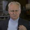
В історії університету є імена, які визначають людське та наукове обличчя закладу на десятиліття вперед. Для Національного технічного університету України "Київський політехнічний інститут ім. Ігоря Сікорського" однією з таких яскравих і фундаментальних особистостей був і залишиться у майбутньому професор Володимир Сергійович Коваленко. 20 червня п.р. виповнилося 85 років від дня народження цього видатного вченого, науково-дослідницька та викладацька діяльність якого була сконцентрована та цілеспрямована, як приборканий ним лазерний промінь.
Ascent reflects on first-half 2026 achievements and milestones
➡️ Реєстрація на відбір до ветеранської магістерської програми за спеціальностями «Прикладна механіка» та «Біомедична інженерія»

Запрошуємо ветеранів і ветеранок зареєструватися для участі у відборі на ветеранську магістерську програму за спеціальностями «Прикладна механіка» та «Біомедична інженерія».
Pages




![[link]](https://i.redd.it/gcbh5g6njidh1.jpeg)